Inquire: Call 0086-755-23203480, or reach out via the form below/your sales contact to discuss our design, manufacturing, and assembly capabilities.
Quote: Email your PCB files to Sales@pcbsync.com (Preferred for large files) or submit online. We will contact you promptly. Please ensure your email is correct.
Notes: For PCB fabrication, we require PCB design file in Gerber RS-274X format (most preferred), *.PCB/DDB (Protel, inform your program version) format or *.BRD (Eagle) format. For PCB assembly, we require PCB design file in above mentioned format, drilling file and BOM. Click to download BOM template To avoid file missing, please include all files into one folder and compress it into .zip or .rar format.
If you’ve ever wondered why some multilayer boards fail during assembly while others survive thousands of thermal cycles, the answer often lies in the lamination process. After 15 years working with PCB fabrication, I can tell you that lamination is where your stackup design either becomes reality or falls apart—literally.
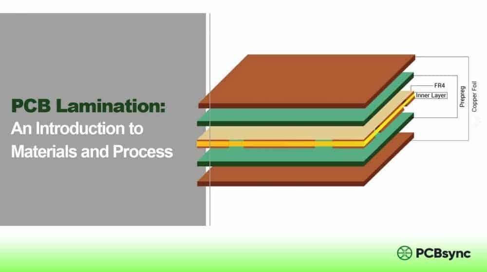
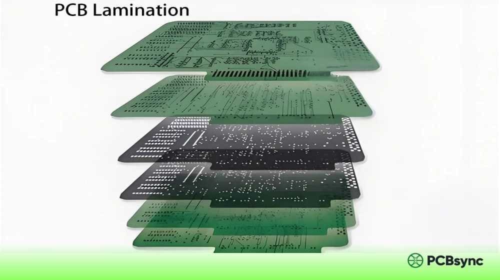
PCB lamination is the manufacturing process that bonds multiple layers of copper foil, prepreg, and core materials together under controlled heat and pressure. This step transforms separate circuit layers into a unified, functional board capable of handling complex routing in everything from smartphones to aerospace systems.
This guide covers everything you need to know about the PCB lamination process—from material selection to troubleshooting common defects. Whether you’re designing a 4-layer prototype or a 20-layer HDI board, understanding lamination will help you make better design decisions and avoid costly manufacturing issues.
PCB lamination permanently bonds together the layers of a multilayer PCB stackup using heat and pressure. During this process, the resin in prepreg materials melts, flows to fill gaps between copper features, and then cures to form rigid dielectric layers that insulate conductors from each other.
Without proper lamination, you’d end up with loose layers that can’t maintain consistent dielectric thickness, controlled impedance, or mechanical integrity. The process directly affects:
Signal integrity: Consistent dielectric thickness maintains impedance control
Reliability: Proper bonding prevents delamination during thermal cycling
Mechanical strength: The cured resin matrix provides structural rigidity
For any board with more than two layers, lamination isn’t optional—it’s the step that makes multilayer routing possible.
Key Materials Used in PCB Lamination
Understanding lamination materials is essential because each component plays a specific role in the final board’s performance. Get the materials wrong, and no amount of process optimization will save your design.
Prepreg (Pre-impregnated Material)
Prepreg is fiberglass cloth impregnated with partially cured (B-stage) epoxy resin. Think of it as the glue that holds everything together. During lamination, the resin melts and flows before cross-linking into a fully cured state.
Key prepreg specifications include:
Resin content: Standard (42-48%), medium (48-52%), or high (52-58%)
Dielectric constant (Dk): Varies with resin content (typically 3.8-4.5 for FR-4)
Higher resin content prepregs flow more during lamination, which helps fill gaps around copper features but can cause thickness variations. I typically specify medium resin content unless the design has heavy copper or dense routing that needs extra fill.
Core (Copper-Clad Laminate)
The core is fully cured laminate with copper foil bonded to one or both sides. Unlike prepreg, cores are rigid and don’t flow during lamination—they maintain their thickness and provide the structural backbone of your stackup.
Core characteristics:
Material grade: FR-4 (standard), high-Tg FR-4, polyimide, Rogers
Copper weight: 0.5 oz (18 μm) to 2 oz (70 μm) standard; heavy copper goes higher
Dielectric thickness: 0.004″ to 0.062″ standard range
Dk stability: Core Dk is stable; prepreg Dk changes after lamination
Copper Foil
Copper foil forms the conductive traces. For lamination purposes, the surface treatment matters most—it determines how well the foil bonds to the resin.
Foil types:
ED (electrodeposited): Standard, matte side bonds to resin
RA (rolled annealed): Better for flex applications
RTF (reverse-treat foil): Smooth side out for better high-frequency performance
HVLP/VLP (very low profile): Reduced roughness for signal integrity above 10 GHz
The lamination method depends on your board’s complexity, layer count, and via structure. Not all lamination is created equal.
Standard Press Lamination
The workhorse method for conventional multilayer PCBs. All layers are stacked and pressed together in a single lamination cycle.
Process parameters:
Temperature: 170-200°C (340-390°F)
Pressure: 200-400 psi (14-28 bar)
Cycle time: 60-120 minutes
Vacuum: Maintained throughout heating
Standard lamination works for boards up to 16-20 layers without blind or buried vias. The entire stackup goes into the press at once, and you get your laminated panel out the other side.
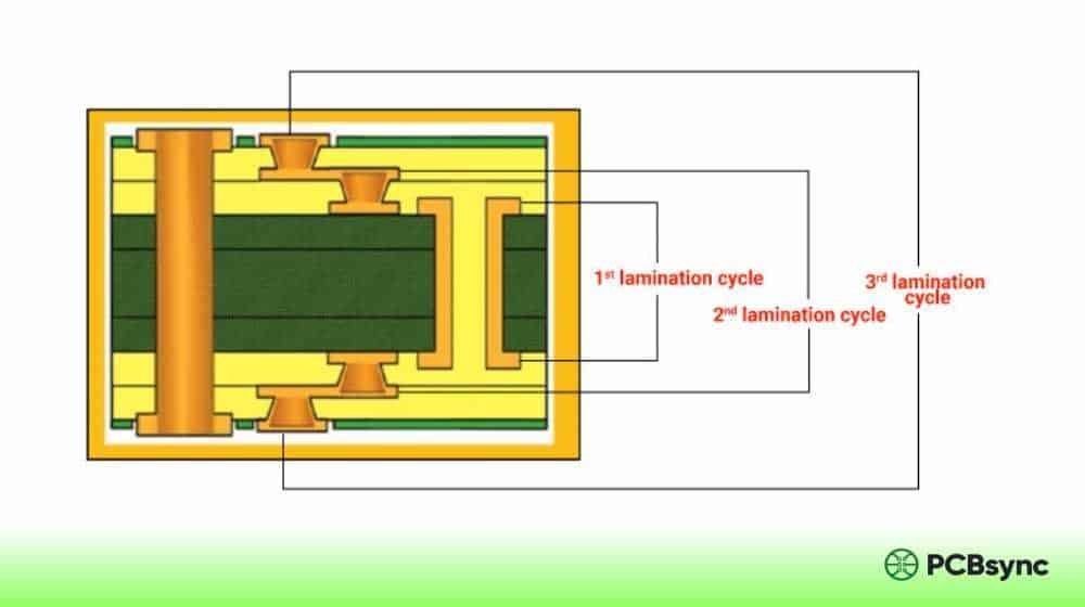
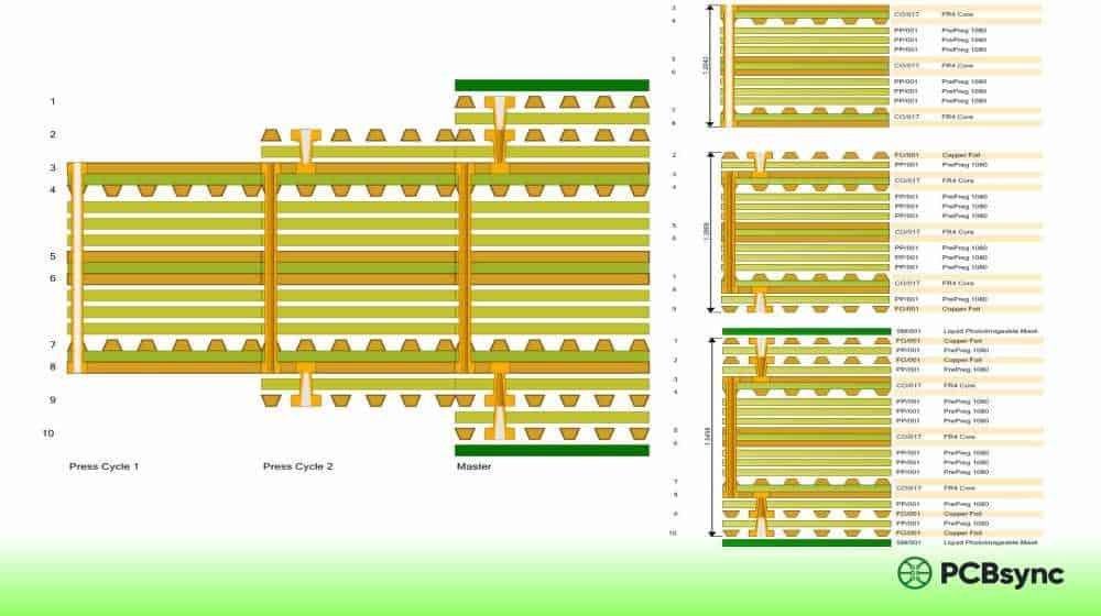
Sequential Lamination
Required for HDI boards with blind vias, buried vias, or complex via structures. The board is built up through multiple lamination cycles, with drilling and plating occurring between cycles.
Example: 8-layer sequential build
Laminate layers 3-4-5-6 as inner core
Drill and plate buried vias (3-6)
Laminate layers 2 and 7 with prepreg
Drill and plate blind vias (2-3, 6-7)
Laminate layers 1 and 8 with prepreg
Drill and plate outer blind vias and through-holes
Each lamination cycle adds cost and lead time but enables routing density that’s impossible with standard methods. I recommend keeping sequential lamination cycles to 2-3 maximum unless your design absolutely requires more.
Vacuum Lamination
Uses a vacuum bag or chamber to apply uniform pressure and remove trapped air. Essential for:
High-layer-count boards (20+ layers)
Boards with large copper areas
High-Tg and low-Dk materials
Any design requiring void-free lamination
Vacuum lamination removes air pockets that would otherwise cause voids, making it the preferred method for aerospace, medical, and high-reliability applications.
PTFE/Teflon Microwave Lamination
RF and microwave boards using PTFE substrates require modified lamination parameters because PTFE doesn’t bond well with standard processes.
PTFE lamination typically costs 3-5x more than standard FR-4 lamination, so hybrid constructions (Rogers on outer layers, FR-4 core) are common for balancing performance and cost.
Step-by-Step PCB Lamination Process
Here’s what actually happens during lamination, from prep through final inspection.
Step 1: Material Preparation
Inner layers are etched with circuit patterns
Copper surfaces receive oxide treatment (brown or black oxide) to improve adhesion
Prepreg is stored in climate-controlled conditions (23°C, <50% RH)
Materials are pre-baked if moisture content exceeds 0.2%
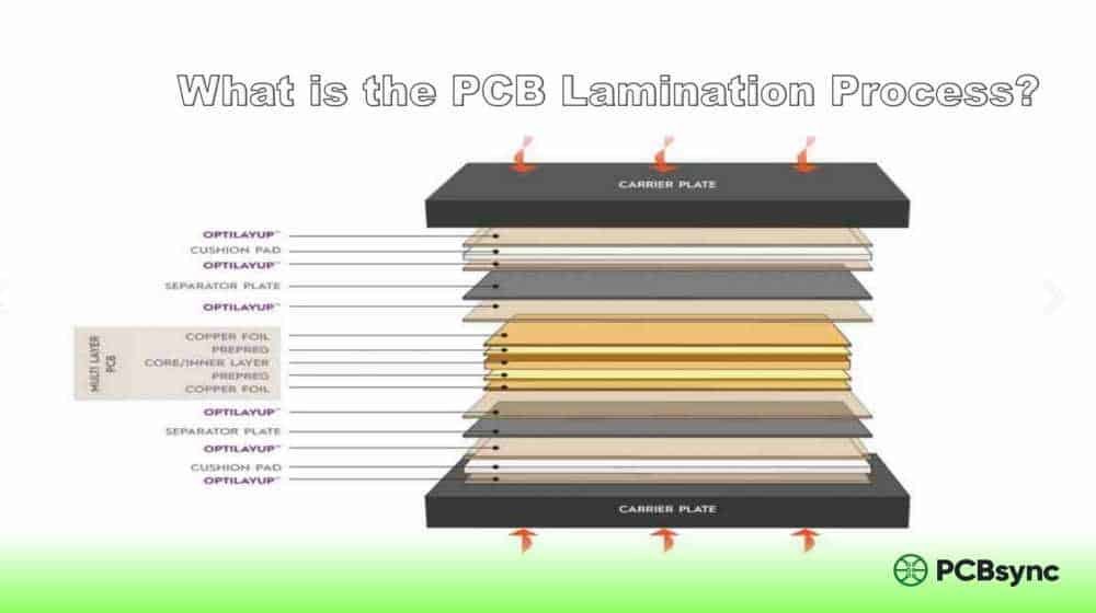
Step 2: Stackup Assembly
Layers are stacked on a heavy steel base plate
Alignment pins or optical registration ensure layer-to-layer accuracy
Prepreg sheets are placed between cores
Copper foil added to outer layers
Release film and press plates complete the “book”
Step 3: Lamination Press Cycle
Stage
Temperature
Pressure
Duration
Purpose
Preheat
80-120°C
Low
10-15 min
Soften resin, remove volatiles
Heat ramp
120-180°C
Increasing
15-20 min
Resin flow begins
Full cure
175-190°C
250-400 psi
45-60 min
Complete cross-linking
Cool down
190°C to 60°C
Maintained
20-30 min
Prevent warpage
The temperature ramp rate is critical—typically 2-3°C per minute. Faster rates cause uneven resin flow; slower rates waste cycle time.
Step 4: Post-Lamination
Panel is removed from press and inspected
Edge trim removes overflow material
Thickness measured at multiple points (target: ±10% of design)
Getting lamination right means controlling these parameters precisely.
Temperature Control
Parameter
Standard FR-4
High-Tg FR-4
Polyimide
Rogers
Peak temp
175-185°C
185-200°C
200-220°C
190-210°C
Ramp rate
2-3°C/min
2-3°C/min
1.5-2°C/min
2-3°C/min
Dwell time
45-60 min
60-90 min
90-120 min
60-90 min
A temperature variation of just 5°C can affect resin flow and cause voids or incomplete cure. Modern lamination presses use multi-zone heating to maintain ±2°C uniformity across the platen.
Pressure Control
Insufficient pressure causes voids and weak bonding. Excessive pressure squeezes out too much resin, causing thin spots and dielectric thickness variation.
Target pressures:
Standard multilayer: 250-350 psi
High-layer-count: 300-400 psi
PTFE materials: 100-200 psi
Heavy copper (3+ oz): 350-400 psi
Vacuum Level
Vacuum removes air that would otherwise form voids. Target is <5 mbar (0.5 kPa) before heat application begins.
Common PCB Lamination Defects and Solutions
Even with controlled parameters, defects happen. Here’s how to identify and prevent the most common issues.
Delamination
What it looks like: Layers separating, visible as blisters or gaps between layers. Often appears after thermal stress (soldering).
Root causes:
Moisture in materials (>0.2% by weight)
Inadequate oxide treatment on copper
Insufficient pressure during lamination
CTE mismatch between materials
Exceeding Tg during assembly
Prevention:
Pre-bake materials (105-125°C for 4-8 hours)
Verify oxide adhesion before lamination
Use high-Tg materials for lead-free assembly
Store laminated boards in moisture barrier bags
Voids and Air Bubbles
What it looks like: Small pockets within dielectric layers, visible on cross-section or X-ray.
Root causes:
Trapped air during stackup
Insufficient vacuum
Low resin content in prepreg
Volatile contamination
Prevention:
Maintain vacuum <5 mbar throughout cycle
Use appropriate resin content for copper density
Ensure clean lamination environment
Optimize temperature ramp to allow complete air evacuation
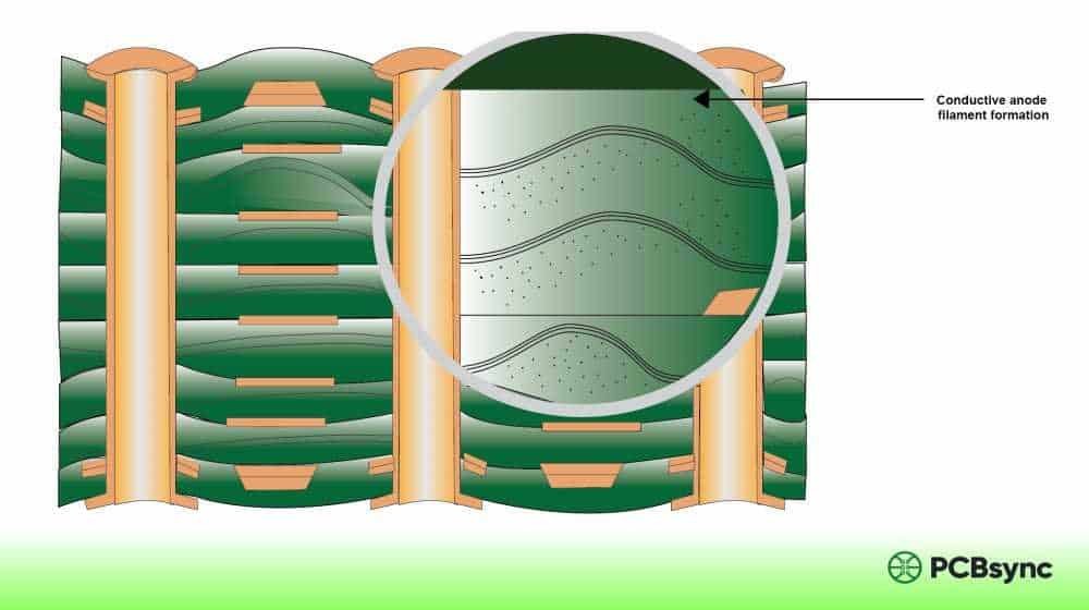
Warpage
What it looks like: Board is curved or twisted instead of flat. IPC-6012 limits warpage to 0.75% of board dimension.
Root causes:
Asymmetric stackup
Uneven copper distribution
Rapid cooling after lamination
CTE mismatch
Prevention:
Design symmetric stackups (balanced copper on each side of center)
Slow cooling rate (3-5°C/min)
Even copper distribution across layers
Pre-bake before assembly
Registration Errors
What it looks like: Layers are misaligned, causing drill breakout or via misses.
Root causes:
Material movement during heat-up
Inadequate pinning during stackup
Different shrinkage rates between materials
Prevention:
Use multiple alignment pins
Control prepreg moisture content
Match material CTE characteristics
Post-etch punch inner layers for registration
PCB Lamination for High-Speed and HDI Designs
High-speed digital and HDI designs push lamination requirements further than standard boards.
Signal Integrity Considerations
At frequencies above 1 GHz, lamination quality directly affects signal integrity:
Dk uniformity: Prepreg Dk varies with resin flow. Specify controlled-flow prepregs for critical layers.
Fiber weave effect: Glass weave pattern can cause skew in differential pairs. Use spread glass or rotate traces.
Sequential Lamination for HDI
HDI stackups require careful planning of lamination cycles:
HDI Type
Structure
Lamination Cycles
Typical Application
Type I
1+N+1
2
Smartphones, tablets
Type II
1+N+1 (buried via)
2-3
Networking equipment
Type III
2+N+2
3-4
High-end computing
Any-layer
Multiple stacked
4+
Advanced packages
Each lamination cycle adds 15-25% to board cost. Work with your fabricator early to optimize the stackup for minimum lamination cycles while meeting routing requirements.
Material Selection for High-Speed
For designs above 10 Gbps, standard FR-4 may not cut it:
Megtron 4/6: Dk 3.4-3.6, Df 0.002-0.004, good for 25+ Gbps
IS415/IS420: Dk 3.45, Df 0.009, balance of performance and cost
Rogers RO4003C: Dk 3.38, Df 0.0027, RF and microwave
Industry Applications of PCB Lamination
Different industries have different lamination requirements based on their reliability and performance needs.
Multiple lamination testing per IPC-6012 Class 3/A
Full traceability of materials and processes
Sequential lamination for complex HDI structures
Automotive Electronics
High-Tg materials for under-hood applications (150°C+ operating)
Enhanced moisture resistance
AEC-Q100 qualified materials
Controlled impedance for ADAS radar
Medical Devices
USP Class VI materials for implantables
Void-free lamination for reliability
Full material traceability
Sterilization-compatible laminate selection
Consumer Electronics
Cost-optimized standard FR-4
HDI lamination for smartphones and tablets
Quick-turn capability for rapid product cycles
Fine-pitch BGA support via sequential lamination
Telecommunications and 5G
The rollout of 5G infrastructure has pushed PCB lamination requirements significantly. Base station equipment operates at millimeter-wave frequencies where even small Dk variations cause performance issues.
5G lamination requirements:
Ultra-low loss materials (Df <0.003)
Tight dielectric thickness control (±5%)
Hybrid constructions (Rogers + FR-4)
Sequential lamination for complex antenna structures
Many 5G antenna boards use modified sequential lamination with different materials on different layer pairs—Rogers for RF layers, high-Tg FR-4 for digital layers. This requires careful planning of lamination cycles and material compatibility.
Advanced Lamination Technologies and Trends
The PCB industry continues to develop new lamination technologies to meet emerging requirements.
Embedded Component Lamination
Passive components (resistors, capacitors) can be embedded within the PCB stackup during lamination. This reduces board area, improves high-frequency performance by shortening interconnects, and increases reliability by eliminating solder joints.
The lamination process for embedded components requires:
Precise cavity formation in core or prepreg
Controlled resin flow to encapsulate components
Modified temperature profiles to avoid component damage
Sequential lamination for multiple embedded layers
Rigid-Flex Lamination
Combining rigid and flexible sections in a single board requires specialized lamination techniques:
No-flow prepregs to prevent resin contamination of flex areas
Selective bonding with adhesive only where needed
Multiple lamination cycles for complex rigid-flex structures
Careful CTE matching between rigid and flex materials
Ultra-High Layer Count
Data center and AI accelerator applications increasingly demand 30+ layer boards with multiple lamination cycles:
40-60 layer designs becoming common for advanced computing
Requires 5-8 lamination cycles with sequential build-up
Warpage control becomes critical with each additional cycle
Lead times extend to 8-12 weeks for complex builds
How to Choose the Right Lamination Method
Your lamination method depends on several design factors:
Use standard lamination when:
Layer count is 16 or fewer
No blind or buried vias required
Standard impedance tolerance (±10%) is acceptable
Cost is a primary concern
Use sequential lamination when:
Design requires blind or buried vias
HDI routing is necessary for fine-pitch components
Layer count exceeds 16-20 layers
High-density BGA fanout is required
Use vacuum lamination when:
High-layer-count (20+ layers)
High-reliability requirement (Class 3)
Low-loss or PTFE materials
Void-free construction is critical
Cost Factors in PCB Lamination
Understanding what drives lamination cost helps you make better design decisions.
Material Costs
Material Type
Relative Cost
When to Use
Standard FR-4
1x (baseline)
General purpose, cost-sensitive
High-Tg FR-4
1.2-1.5x
Lead-free assembly, automotive
Low-loss FR-4 (IS415)
1.5-2x
High-speed digital, 10+ Gbps
Megtron 4/6
3-5x
Ultra-high-speed, 25+ Gbps
Rogers 4003C
5-8x
RF/microwave, antennas
PTFE (Rogers 5880)
8-12x
Millimeter-wave, satellite
Process Cost Multipliers
Sequential lamination: Each cycle adds 15-25% to base cost
Hybrid construction: Mixed materials add 20-40%
Vacuum lamination: Adds 10-15% for standard materials
Minimize lamination cycles: Redesign via structure if possible
Use hybrid stackups: Low-loss material only where needed
Standardize on common materials: Fabricator stock items cost less
Panel size optimization: Better material utilization reduces waste
Design for manufacturability: Reduce complexity where possible
Best Practices for Successful PCB Lamination
After working on hundreds of multilayer designs, these practices consistently produce better lamination results.
Design Phase Best Practices
Balance your stackup. Asymmetric copper distribution is the number one cause of warpage. Mirror your copper density above and below the center plane. If layer 2 has a 70% copper pour, layer 7 should have similar coverage.
Specify materials early. Don’t design for generic “FR-4” and expect your fabricator to figure it out. Choose specific laminate grades based on your Tg, Dk, and Df requirements. Different material families have different lamination parameters.
Plan your via structure with lamination in mind. Buried vias between layers 3-6 in an 8-layer board require different lamination sequencing than buried vias between 2-7. Work backward from your via requirements to determine the minimum lamination cycles needed.
Communicate dielectric requirements clearly. If you need 5.0 mil dielectric between layers 3 and 4 for impedance control, specify it. If you can tolerate variation, say so—it gives the fabricator flexibility to optimize their process.
Working with Your Fabricator
Submit your stackup for review before finalizing your design. Most fabricators offer free stackup review. They can identify lamination issues before you commit to a design that’s difficult or expensive to manufacture.
Ask about their standard materials. Using materials the fabricator stocks reduces lead time and cost. Custom materials may require minimum order quantities and extended procurement time.
Understand their lamination capabilities. Not all fabricators can handle 20+ layer sequential lamination or hybrid material constructions. Match your design complexity to your fabricator’s capabilities.
Request cross-section analysis for critical designs. For impedance-critical or high-reliability boards, a cross-section of the laminated panel confirms dielectric thickness and void-free construction.
Quality Control Checks
After lamination, verify these parameters:
Check
Method
Accept Criteria
Total thickness
Micrometer
±10% of design
Warpage
Flatness gauge
<0.75% per IPC-6012
Dielectric thickness
Cross-section
±10% of specified
Voids
X-ray or SAM
None in active area
Registration
X-ray
Within drill tolerance
Delamination
Visual/thermal stress
None after 288°C solder float
Useful Resources for PCB Engineers
Here are some references I’ve found valuable for lamination specifications and material selection:
IPC Standards:
IPC-4101: Specification for Base Materials for Rigid and Multilayer Printed Boards
IPC-6012: Qualification and Performance Specification for Rigid Printed Boards
IPC-2221: Generic Standard on Printed Board Design
Polar Instruments Si9000: Impedance calculation with laminate properties
Altium Designer: Stackup planning with manufacturer data
Technical Resources:
Sierra Circuits Design Guides: protoexpress.com/blog
Altium Resources: resources.altium.com
Frequently Asked Questions About PCB Lamination
What temperature is used for PCB lamination?
Standard FR-4 lamination uses peak temperatures of 175-190°C (347-374°F). High-Tg materials require 185-200°C, while polyimide may need 200-220°C. The entire thermal cycle, including preheat, dwell, and cooling, typically takes 90-120 minutes. Temperature ramp rates of 2-3°C per minute are standard to ensure even resin flow.
What causes delamination in PCBs?
The most common cause is moisture trapped in the prepreg or core materials, which turns to steam during soldering and creates pressure that separates layers. Other causes include inadequate oxide treatment on inner layer copper, insufficient lamination pressure, and thermal stress from exceeding the material’s Tg during assembly. Pre-baking materials and using high-Tg laminates for lead-free assembly prevents most delamination issues.
How many lamination cycles are needed for HDI PCBs?
A standard 1+N+1 HDI requires 2 lamination cycles. More complex structures like 2+N+2 need 3-4 cycles, and any-layer HDI may require 4 or more. Each cycle adds roughly 15-25% to board cost and extends lead time, so designers should minimize cycles while meeting routing requirements. Most HDI designs can be achieved with 2-3 lamination cycles.
What’s the difference between prepreg and core in PCB lamination?
Core is fully cured laminate with copper on one or both sides—it’s rigid and maintains its thickness during lamination. Prepreg is partially cured (B-stage) material that flows and bonds layers together when heated. The key difference is that core Dk is stable, while prepreg Dk changes after lamination due to resin flow. For impedance-critical designs, understanding this Dk variation is essential for accurate modeling.
Can FR-4 be used for high-frequency PCBs?
Standard FR-4 works adequately up to about 1-2 GHz but becomes problematic at higher frequencies due to its relatively high Dk (4.2-4.5) and high loss tangent (Df 0.02). Above 6 GHz, the losses become significant enough to require specialized materials like Rogers, Taconic, or Isola’s low-loss laminates. Hybrid constructions using Rogers on outer layers with FR-4 cores offer a cost-effective compromise for many RF designs.
Conclusion
PCB lamination is the process that transforms your stackup design into a functional multilayer board. Getting it right requires understanding materials, controlling process parameters, and matching your lamination method to your design requirements.
The key takeaways:
Material selection determines lamination parameters and final board performance
Process control (temperature, pressure, vacuum) prevents defects
Sequential lamination enables HDI but adds cost and complexity
Work with your fabricator early to optimize stackup for manufacturability
Whether you’re designing a cost-sensitive consumer product or a high-reliability aerospace system, understanding lamination helps you make better design decisions and avoid costly pcb manufacturing issues.
Inquire: Call 0086-755-23203480, or reach out via the form below/your sales contact to discuss our design, manufacturing, and assembly capabilities.
Quote: Email your PCB files to Sales@pcbsync.com (Preferred for large files) or submit online. We will contact you promptly. Please ensure your email is correct.
Notes: For PCB fabrication, we require PCB design file in Gerber RS-274X format (most preferred), *.PCB/DDB (Protel, inform your program version) format or *.BRD (Eagle) format. For PCB assembly, we require PCB design file in above mentioned format, drilling file and BOM. Click to download BOM template To avoid file missing, please include all files into one folder and compress it into .zip or .rar format.


