Inquire: Call 0086-755-23203480, or reach out via the form below/your sales contact to discuss our design, manufacturing, and assembly capabilities.
Quote: Email your PCB files to Sales@pcbsync.com (Preferred for large files) or submit online. We will contact you promptly. Please ensure your email is correct.
Notes: For PCB fabrication, we require PCB design file in Gerber RS-274X format (most preferred), *.PCB/DDB (Protel, inform your program version) format or *.BRD (Eagle) format. For PCB assembly, we require PCB design file in above mentioned format, drilling file and BOM. Click to download BOM template To avoid file missing, please include all files into one folder and compress it into .zip or .rar format.
PCB Impedance Control Explained: Design, Calculation & Best Practices
If you’ve ever dealt with a high-speed PCB that mysteriously failed EMC testing, or watched USB data packets drop for no apparent reason, you’ve likely run into impedance mismatch issues. I’ve been there—staring at an oscilloscope wondering why my carefully routed differential pairs looked like garbage.
PCB impedance control isn’t just another design checkbox. It’s the difference between a board that works reliably and one that becomes an expensive paperweight. In this guide, I’ll walk you through everything from basic concepts to practical calculations, covering the impedance values you’ll encounter in real-world designs—from 25Ω RF traces to 125Ω specialty applications.
Impedance control is the practice of designing and manufacturing PCB traces so they present a specific, consistent electrical impedance to high-frequency signals. Think of it this way: when your signal frequency gets high enough (generally above 100MHz), your PCB traces stop acting like simple wires and start behaving like transmission lines.
At that point, the trace’s physical geometry—its width, thickness, and distance from reference planes—determines how much the trace “resists” the flow of alternating current. This resistance to AC is what we call impedance, measured in ohms (Ω).
When impedance varies along a trace’s path, part of the signal reflects back toward the source instead of continuing to the destination. These reflections interfere with the original signal, causing ringing, jitter, timing errors, and ultimately data corruption. Controlled impedance eliminates this problem by keeping the trace impedance uniform from source to load.
PCB Impedance Calculator
Calculate trace impedance for controlled impedance PCB designs
Input Parameters
Common Dielectric Constants (εr)
Calculation Results
Common Target Impedances
USB 2.090Ω diff
USB 3.090Ω diff
HDMI100Ω diff
Ethernet100Ω diff
DDR440Ω SE
PCIe85Ω diff
Formula
Select a trace type
⚠️
Results are approximations based on IPC-2141A. For production, verify with your PCB manufacturer. Solder mask effects not included for outer layers.
Why Impedance Control Matters for Modern PCB Designs
Here’s a reality check: almost every modern electronic device uses interfaces that require impedance control. USB, HDMI, PCIe, DDR memory, Ethernet, SATA—they all have strict impedance requirements. Miss those targets, and your product fails compliance testing.
Signal Integrity
Impedance mismatches cause signal reflections. At multi-gigabit speeds, even a 5Ω mismatch can produce reflections strong enough to corrupt data. A USB 3.0 interface running at 5Gbps has zero tolerance for sloppy impedance control.
EMI and Compliance
Poor impedance control doesn’t just hurt your signals—it also radiates electromagnetic interference. Signal reflections create standing waves that turn your PCB traces into unintentional antennas. This makes passing EMC certification significantly harder.
Reliable Power Transfer
Maximum signal power transfers only when source, trace, and load impedances match. Mismatches waste energy as heat and reflected power, reducing system efficiency and potentially causing long-term reliability issues.
Key Factors That Affect PCB Impedance
Understanding what controls impedance is fundamental to getting your design right. Four primary factors determine the characteristic impedance of a PCB trace:
Trace Width
Wider traces have lower impedance; narrower traces have higher impedance. This is typically your primary adjustment variable. For a 50Ω microstrip on standard FR-4, you might use a 6-8 mil trace width, while 100Ω differential pairs often require 4-5 mil traces with tight spacing. Manufacturing tolerances on trace width (typically ±10%) directly impact your final impedance.
Dielectric Height (Distance to Reference Plane)
The distance between your signal trace and the nearest ground or power plane is directly proportional to impedance. Increase the dielectric height, and impedance goes up. This is why your stack-up design is so critical—layer spacing determines what trace widths are achievable for your target impedance.
Dielectric Constant (Dk)
The dielectric constant of your PCB material affects how electromagnetic fields propagate through it. Standard FR-4 has a Dk around 4.2-4.5, which works fine for most designs below 5-6 GHz. For higher frequencies, you’ll need low-Dk materials like Rogers (Dk ~3.0-3.5) to maintain signal integrity and achieve desired impedance values.
Copper Thickness
Trace thickness has a secondary but measurable effect on impedance. Standard 1oz copper (1.4 mils or 35μm) is typical for signal layers. Thicker copper slightly reduces impedance and is often used on power layers rather than signal layers.
Different trace configurations have different impedance behaviors. Understanding which type you’re working with is essential for accurate calculations.
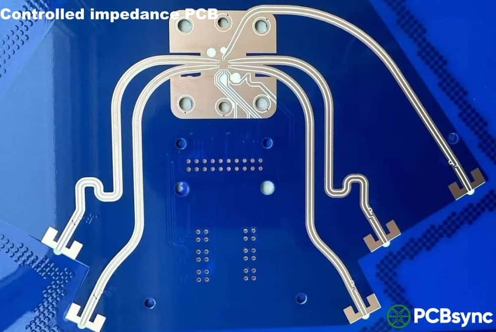
Microstrip
A microstrip is a trace on an outer PCB layer with a single reference plane below it. It’s the most common configuration because outer-layer traces are easy to route and probe for testing. The downside is that microstrips are more susceptible to external interference and EMI radiation compared to striplines. Solder mask covering the trace slightly affects impedance (typically reducing it by 1-3Ω), so calculations should account for coated vs. uncoated configurations.
Stripline
A stripline is a trace buried between two reference planes on inner layers of the PCB. This “sandwiched” configuration provides excellent shielding from interference and produces less radiated EMI. Striplines are ideal for sensitive analog signals and high-speed digital traces where noise immunity is critical. The trade-off is slightly higher signal loss due to the trace being fully embedded in dielectric material.
Differential Pairs
Differential pairs consist of two traces carrying equal and opposite signals. They’re the backbone of modern high-speed interfaces like USB, HDMI, PCIe, and Ethernet. Differential signaling provides superior noise immunity because common-mode interference affects both traces equally and gets cancelled out at the receiver. For differential pairs, you need to control both the single-ended impedance of each trace and the differential impedance of the pair—these are related but distinct values.
Coplanar Waveguide
Coplanar waveguides have ground traces running parallel to the signal trace on the same layer. This configuration is common in RF designs where you need controlled impedance but also need to bring ground references close to signal traces for proper termination at component pads. Coplanar structures can be used with or without a ground plane below.
Common Impedance Values by Application (25Ω to 125Ω)
Different applications demand different impedance values. Here’s a comprehensive reference covering the range from 25Ω to 125Ω:
Interface/Application
Single-Ended (Ω)
Differential (Ω)
Tolerance
RF/Microwave (Low Z)
25-40
—
±5%
Standard RF/General
50
—
±10%
DDR Memory (Data/Addr)
50
100 (clock)
±10%
Video (Analog)
75
—
±10%
PCIe
—
85
±10%
USB 2.0/3.0
45
90
±10-15%
HDMI
50
100
±10%
Gigabit Ethernet
50
100
±10%
LVDS
50
100
±10%
CAN Bus
60
120
±10%
RS-485/422
—
100-120
±10%
How to Calculate PCB Impedance
While complex formulas exist for impedance calculation, in practice you’ll use impedance calculators or field solver software. The key is understanding which inputs matter and how to iterate to your target value.
Simplified Microstrip Formula
For a rough estimate of single-ended microstrip impedance:
Z₀ ≈ (87 / √(εr + 1.41)) × ln(5.98H / (0.8W + T))
Where: Z₀ = characteristic impedance (Ω), εr = dielectric constant, H = dielectric height (mils), W = trace width (mils), T = trace thickness (mils)
Differential Impedance Relationship
For loosely coupled differential pairs (where spacing is large relative to trace width), differential impedance is approximately twice the single-ended impedance: Zdiff ≈ 2 × Z₀. For tightly coupled pairs, mutual coupling between traces reduces this value. A common design approach: target slightly higher single-ended impedance (e.g., 55Ω) so that after coupling, the differential impedance hits exactly 100Ω.
Using Impedance Calculators Effectively
Most PCB manufacturers and EDA tools provide impedance calculators. Here’s a practical workflow:
Start with your manufacturer’s standard stack-up options—these are proven and cost-effective.
Enter the dielectric constant (Dk) for your material. For FR-4, use 4.2-4.5 depending on the specific grade.
Input the dielectric height from your stack-up (distance to reference plane).
Set your target impedance and let the calculator solve for trace width.
Verify the calculated trace width is manufacturable (typically 4-8 mils minimum for most fabs).
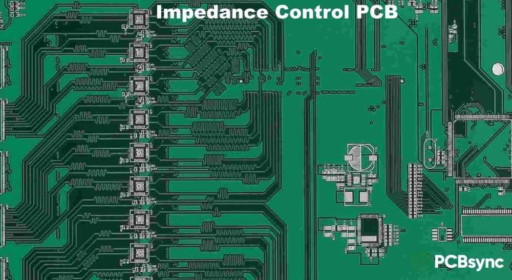
Stack-Up Design for Impedance Control
Your PCB stack-up is the foundation of impedance control. A well-designed stack-up makes hitting your impedance targets straightforward; a poorly designed one makes it nearly impossible.
Stack-Up Best Practices
Place high-speed signal layers adjacent to ground planes. A solid, uninterrupted ground plane provides a clean return path and stable reference for impedance control.
Use symmetric stack-ups for multi-layer boards. This prevents warping during PCB manufacturing and ensures consistent dielectric thicknesses.
Avoid routing high-speed traces on layers far from planes. The greater the distance to the reference plane, the harder it becomes to achieve low impedance with manufacturable trace widths.
Consider signal layer separation. For stripline configurations, the distance to both reference planes affects impedance—asymmetric spacing complicates calculations.
Coordinate with your manufacturer early. They know their standard materials and can suggest stack-ups optimized for your impedance requirements.
Example 4-Layer Stack-Up for 50Ω/100Ω Impedance
Layer
Type
Thickness
Notes
L1 (Top)
Signal (Microstrip)
1oz (1.4 mil)
High-speed signals
Prepreg
Dielectric
~4-5 mil
Dk ≈ 4.2
L2
Ground Plane
1oz (1.4 mil)
Reference for L1
Core
Dielectric
~40 mil
Main structural layer
L3
Power Plane
1oz (1.4 mil)
Reference for L4
Prepreg
Dielectric
~4-5 mil
Dk ≈ 4.2
L4 (Bot)
Signal (Microstrip)
1oz (1.4 mil)
High-speed signals
Manufacturing and Testing Considerations
TDR Testing and Test Coupons
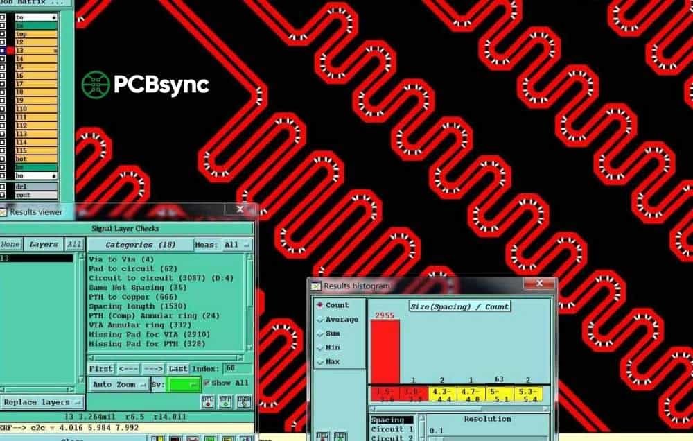
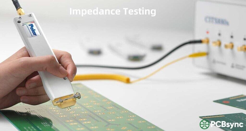
Time Domain Reflectometry (TDR) is the standard method for validating impedance after manufacturing. A TDR instrument sends a fast-rise-time pulse down the trace and measures reflections to determine impedance at each point along the path. Rather than testing every trace on every board (impractical), manufacturers use test coupons—small sections fabricated on the same panel that replicate your controlled impedance structures. If the coupon passes, the boards on that panel should meet spec.
Realistic Tolerance Expectations
The industry standard tolerance for controlled impedance is ±10%. Here’s what to expect:
±10% standard: Achievable with most manufacturers using standard processes. A 50Ω target means actual impedance between 45Ω and 55Ω.
±7-8% tighter tolerance: Available from quality manufacturers with process controls. May cost slightly more.
±5% or tighter: Required for critical RF applications. Significantly increases cost and may require specialized materials.
Don’t specify tighter than needed. Unnecessary tight tolerances increase scrap rates and costs without improving your product’s performance.
Specifying Requirements to Your Manufacturer
Clear documentation prevents manufacturing delays. Include the following in your fabrication notes:
Target impedance value (e.g., 50Ω single-ended, 100Ω differential)
Tolerance required (±10% unless you have a specific reason for tighter)
Which layers require controlled impedance
Trace widths and spacing for controlled traces
Reference plane layer for each signal layer
Whether impedance testing is required (TDR coupon verification)
Best Practices and Common Mistakes to Avoid
PCB板內阻抗測試的方法
Design Best Practices
Route over continuous reference planes. Avoid crossing splits or voids in ground/power planes—this disrupts the return path and causes impedance discontinuities.
Keep trace widths consistent. Abrupt width changes cause reflections. If you must change width (e.g., at BGA breakout), use gradual tapers.
Use 45° or curved bends, not 90° corners. Sharp corners introduce localized impedance changes and can radiate EMI.
Match differential pair lengths. Use serpentine routing on the shorter trace to ensure both signals arrive simultaneously. Keep length matching within 5 mils for high-speed interfaces.
Add stitching vias near layer transitions. When a signal changes layers, add ground vias near the signal via to provide a return path between reference planes.
Aim for wider rather than narrower traces. If your calculation gives borderline trace widths, design slightly wider. Narrower traces hit manufacturing limits and are harder to etch consistently.
Common Mistakes That Cause Impedance Problems
Conflicting documentation. Stack-up views that don’t match fabrication notes cause manufacturing holds and delays. Double-check consistency.
Specifying multiple trace widths for the same impedance on the same layer. Only one trace width can achieve a given impedance on a given layer. Pick one.
Ignoring solder mask effects. Solder mask over microstrips changes impedance by 1-3Ω. Use coated microstrip calculations when applicable.
Not communicating with your manufacturer. Every fab has preferred stack-ups and materials. Designing in isolation often leads to costly stack-up changes later.
Overlooking via discontinuities. Vias introduce impedance spikes. For very high-speed designs (10+ Gbps), consider via backdrilling to reduce stub effects.
Frequently Asked Questions
1. When do I need controlled impedance on my PCB?
You need controlled impedance when signal frequencies exceed approximately 100MHz, or when the trace length is longer than 1/6 of the signal’s rise time converted to distance. Practically speaking, if you’re using USB, HDMI, DDR memory, Ethernet, PCIe, or any modern high-speed interface, you need controlled impedance.
2. Why is 50Ω the most common impedance value?
50Ω represents a historical compromise between power handling capability and signal attenuation. It’s easy to achieve with standard PCB materials and trace geometries, and most RF/microwave equipment is designed around 50Ω systems. For differential signaling, 100Ω (essentially two 50Ω traces) became the de facto standard.
3. Can I use different impedance values on different layers?
Yes, and this is common in multi-layer designs. Different layers have different distances to reference planes, which naturally leads to different trace widths for the same impedance. Just ensure your fabrication documentation clearly specifies the impedance requirements for each layer.
4. How accurate are online impedance calculators?
Online calculators provide reasonable estimates (typically within 5-10% of actual values) for standard configurations. However, they often ignore factors like solder mask, copper roughness, and frequency-dependent dielectric properties. For production boards, use your manufacturer’s calculations or a professional field solver like Polar SI9000.
5. What happens if my impedance is slightly out of spec?
Minor deviations (within ±10%) usually won’t cause immediate failures but may reduce noise margin. Larger deviations cause measurable signal integrity problems: increased jitter, bit errors, and failed compliance testing. For safety-critical or high-reliability applications, staying within spec is non-negotiable.
Useful Resources
Free Impedance Calculators:
Sierra Circuits Impedance Calculator (comprehensive, includes crosstalk)
RAYPCB Impedance Calculator (simple, works with their stack-ups)
Saturn PCB Design Toolkit (free download, includes many tools)
Altium Designer Layer Stack Manager (built-in field solver for Altium users)
Industry Standards:
IPC-2141: Controlled Impedance Circuit Boards and High-Speed Logic Design
IPC-2221: Generic Standard on Printed Board Design
“High-Speed Digital Design” by Howard Johnson (the classic reference)
“Signal and Power Integrity – Simplified” by Eric Bogatin
“Transmission Line Design Handbook” by Brian C. Wadell
Wrapping Up
PCB impedance control isn’t something you can afford to treat as an afterthought. As signal speeds continue climbing and board densities increase, the margin for error keeps shrinking. The good news is that getting it right isn’t magic—it’s engineering.
Start with a solid stack-up, use the right calculations for your trace geometries, work closely with your manufacturer, and verify your designs with TDR testing. Follow the best practices outlined here, avoid the common mistakes, and your high-speed interfaces will work as intended—every time.
Questions about impedance control for your specific application? Drop a comment below or reach out—I’m always happy to discuss real-world design challenges.
Inquire: Call 0086-755-23203480, or reach out via the form below/your sales contact to discuss our design, manufacturing, and assembly capabilities.
Quote: Email your PCB files to Sales@pcbsync.com (Preferred for large files) or submit online. We will contact you promptly. Please ensure your email is correct.
Notes: For PCB fabrication, we require PCB design file in Gerber RS-274X format (most preferred), *.PCB/DDB (Protel, inform your program version) format or *.BRD (Eagle) format. For PCB assembly, we require PCB design file in above mentioned format, drilling file and BOM. Click to download BOM template To avoid file missing, please include all files into one folder and compress it into .zip or .rar format.


