Inquire: Call 0086-755-23203480, or reach out via the form below/your sales contact to discuss our design, manufacturing, and assembly capabilities.
Quote: Email your PCB files to Sales@pcbsync.com (Preferred for large files) or submit online. We will contact you promptly. Please ensure your email is correct.
Notes: For PCB fabrication, we require PCB design file in Gerber RS-274X format (most preferred), *.PCB/DDB (Protel, inform your program version) format or *.BRD (Eagle) format. For PCB assembly, we require PCB design file in above mentioned format, drilling file and BOM. Click to download BOM template To avoid file missing, please include all files into one folder and compress it into .zip or .rar format.
If you’ve ever worked with edge connectors—RAM modules, graphics cards, PCI Express cards—you know how critical a smooth insertion is. A PCB that jams or scrapes during connection isn’t just frustrating; it can damage both the board and the receiving slot. That’s where gold finger beveling comes in.
As a PCB engineer who has dealt with countless connector-related failures, I can tell you that beveling is one of those “small details” that makes a massive difference in product reliability. In this guide, I’ll walk you through everything you need to know about gold finger beveling: why it matters, the right angles to use, the manufacturing process, and the design rules that will save you from costly rework.
Minimal (~$0.02-0.05 per board for standard beveling)
Design impact
Requires specific clearances and inner-layer copper removal
Now let’s get into the details that will help you design better boards and avoid common pitfalls.
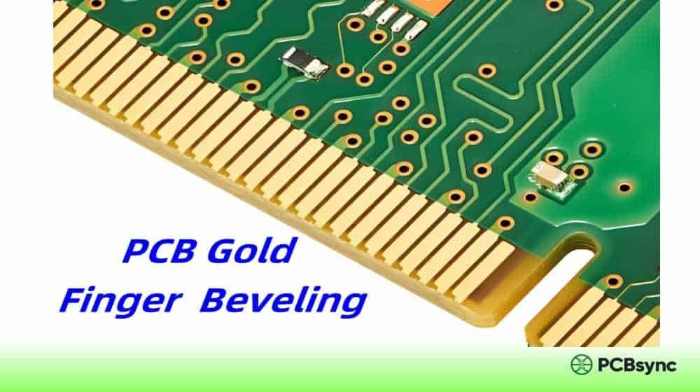
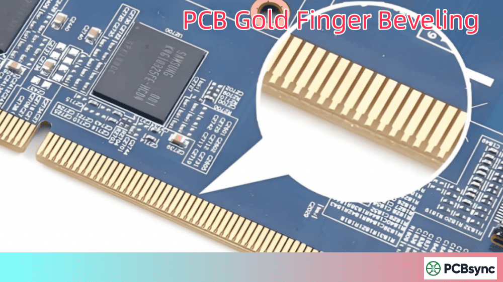
What Is Gold Finger Beveling?
Gold finger beveling is a mechanical finishing process that transforms the sharp, 90-degree edges of PCB gold fingers into angled, sloped surfaces. Instead of a blunt edge that catches on connector pins, a beveled edge creates a smooth ramp that guides the board into place.
Think of it like this: try sliding a book with a squared-off edge into a tight slot versus one with a tapered edge. The tapered version glides in effortlessly. That’s exactly what beveling does for your PCB.
The process happens after gold plating is complete, typically using CNC grinding or precision milling equipment. The result is a chamfered edge—usually at 30 to 45 degrees—that reduces insertion force and prevents mechanical damage during the hundreds or thousands of plug-in cycles your product might experience.
Why Beveling Is Not Optional
I’ve seen engineers skip beveling to save a few cents per board. Here’s what typically happens:
Difficult insertion – Operators struggle to plug in boards, leading to assembly delays
Connector pin damage – Sharp edges scratch or bend the receiving socket’s contact pins
Signal integrity issues – Damaged contacts lead to intermittent connections and data errors
One client came to me after experiencing a 15% field failure rate on their industrial control modules. The root cause? Unbeveled gold fingers that had worn down their backplane connectors. The fix was simple but the lesson was expensive.
Before diving deeper into beveling, let’s establish what we’re working with.
What Are Gold Fingers?
Gold fingers are the gold-plated contact pads arranged in a row along the edge of a PCB. They serve as the electrical and mechanical interface when the board is inserted into a mating connector or slot.
The gold plating isn’t pure gold—it’s an electroplated hard gold alloy containing 5-10% cobalt. This cobalt-hardened gold provides the wear resistance needed for repeated insertion and removal cycles. According to IPC-4556, the typical gold thickness ranges from 3µ” to 50µ” (microinches), with 30-50µ” being standard for high-reliability applications.
Types of Gold Fingers
Type
Description
Common Use Cases
Normal (Even)
All fingers have identical length, width, and spacing
Standard RAM, most PCIe cards
Uneven (Staggered)
Same width but different lengths
Hot-swap designs, power sequencing
Segmented
Multiple rows at different positions
Complex multi-channel connectors
Graded
Varying plating depths for contact sequencing
High-reliability industrial systems
The longer-then-shorter finger arrangement isn’t just for looks. It ensures ground and power pins make contact before data lines, protecting sensitive circuits from ESD and voltage spikes during hot insertion.
Gold Finger Bevel Angles: Choosing the Right One
The bevel angle directly impacts insertion force, contact alignment, and long-term reliability. Here’s what works and when to use each option.
Most common choice – general-purpose edge connectors
45°
Lower
Reduced
High-density connectors, frequent plug/unplug
60°
Very low
Minimal
Specialized applications only
The 30-Degree Standard
For about 80% of applications, 30 degrees is your go-to angle. It offers the best balance between easy insertion and maintaining enough contact surface for reliable electrical connection.
I recommend 30° as your default unless you have specific reasons to deviate:
Use 45° when you need reduced insertion force (useful for high-density connectors like DDR5 DIMM slots or when operators frequently swap modules)
Use 20° when contact stability is paramount and the board won’t be removed often (permanent installations, embedded systems)
Calculating Bevel Depth
The bevel depth depends on your board thickness. Here’s a practical reference:
Board Thickness
Typical Bevel Depth
Residual Thickness
0.8mm
0.15-0.20mm
0.60-0.65mm
1.0mm
0.20-0.25mm
0.75-0.80mm
1.6mm
0.50-0.60mm
1.00-1.10mm
2.0mm
0.65-0.75mm
1.25-1.35mm
The formula for calculating bevel depth:
d = (t – tr) / cos(θ)
Where:
d = bevel depth
t = board thickness
tr = residual thickness after beveling
θ = bevel angle
Your fab house will typically specify minimum residual thickness around 0.5mm to maintain mechanical integrity. Never bevel so deeply that you compromise the board’s structural strength at the connector edge.
The Gold Finger Beveling Process: Step by Step
Understanding the manufacturing sequence helps you design for manufacturability and anticipate potential issues.
Step 1: PCB Fabrication
The base PCB is manufactured with proper trace routing and copper patterns. The gold finger areas are defined in the outer layer artwork, with appropriate clearances from solder mask and silkscreen.
Step 2: Nickel Plating
Before gold, a nickel underlayer (3-6 microns thick, approximately 150-200 microinches) is electroplated onto the copper finger pads. Nickel serves three purposes:
Acts as a diffusion barrier preventing copper migration into gold
Provides a hard, smooth surface for gold adhesion
Adds additional wear resistance beneath the gold layer
Step 3: Hard Gold Plating
Hard gold (1-2 microns, typically 30-50 microinches for commercial applications) is electroplated over the nickel. The gold alloy contains 5-10% cobalt for enhanced hardness and wear resistance.
Step 4: Solder Mask Application
The solder mask is applied to the board, carefully avoiding the gold finger areas. A minimum clearance of 0.5-1.0mm should exist between the solder mask edge and the gold fingers.
Step 5: Beveling
This is where the magic happens. The beveling process uses specialized equipment:
Fully Automatic Beveling Machines:
CNC-controlled precision grinding
Capable of selective beveling (different edges, different angles)
Required when gold fingers are oriented in different directions
Typical tolerance: ±2°
Semi-Automatic Beveling:
Cuts the entire board edge at once
Lower cost for simple, single-edge beveling
Adequate for most standard applications
The machine removes material at the specified angle while avoiding damage to the gold plating. A properly calibrated machine will bevel right up to the finger edge without cutting into the plated area.
Step 6: Cleaning and Inspection
Post-beveling, boards are cleaned to remove debris and inspected for:
Correct bevel angle (measured with optical inspection systems)
Smooth, burr-free edges
No damage to gold plating
Uniform bevel depth across all fingers
Critical Design Rules for Gold Finger Beveling
These rules aren’t suggestions—they’re requirements. Violating them will result in pcb manufacturing issues, rejected boards, or field failures.
Mandatory Spacing Requirements
Clearance
Minimum Distance
Reason
PTH to gold fingers
1.0mm
Prevents copper contamination during plating
SMD pads to gold fingers
1.0mm
Avoids solder bridging and plating issues
Board outline to gold fingers
0.5mm
Ensures bevel doesn’t cut into fingers
Solder mask to gold fingers
0.5mm
Prevents mask overflow onto contact surfaces
Silkscreen to gold fingers
1.0mm
Keeps printing clear of contact area
Inner Layer Copper Rules
This one trips up even experienced designers: inner layers must be copper-free beneath the gold finger area, extending at least 0.6mm (for 1.6mm boards) beyond the bevel line.
Why? During beveling, the grinding process exposes the board edge. If copper exists on inner layers, it becomes visible—both an aesthetic issue and a potential reliability concern (exposed copper can oxidize).
For a 1.6mm thick board with 30° bevel, ensure no copper on inner layers within 0.6mm of the board edge. For 2.0mm boards, extend this to 0.75mm.
Gold Finger Orientation
Gold fingers must face outward from the PCB center. This isn’t arbitrary—it’s a manufacturing requirement. Beveling machines approach from the board edge, and inward-facing fingers cannot be properly beveled.
If your design requires fingers on multiple edges or in unusual orientations, coordinate with your fab house early. Some configurations require fully-automatic equipment and cost more.
Maximum Finger Length
Keep gold fingers under 40mm in length. Longer fingers are prone to:
Plating uniformity issues
Mechanical damage during handling
Insertion alignment problems
If you need longer contact areas, consider segmented finger designs or alternative connector approaches.
Minimum Board Width for Beveling
Most beveling equipment requires a minimum board width of 45-50mm perpendicular to the beveled edge. Narrower boards can’t be properly fixtured in standard machines. If your design is smaller, discuss panelization options with your manufacturer.
Common Gold Finger Beveling Problems and Solutions
Even with good design, issues can arise. Here’s how to identify and fix the most common problems.
Problem 1: Uneven Bevel Angle
Symptoms: Variable insertion force across the board, some areas of the finger edge are sharper than others
Causes:
Worn cutting tools
Machine calibration drift
Inconsistent board thickness
Solutions:
Specify tighter angle tolerance in fabrication notes (±2° is achievable)
Request measurement data from the fab house
Consider boards from a single lot for critical applications
Require secondary polishing or deburring in your fab notes
Request close-up photos of the beveled edge before shipment
Add cleaning specification to your inspection criteria
Problem 4: Connector Pin Damage
Symptoms: Bent or scratched pins in receiving connector, poor contact reliability
Causes:
Insufficient bevel angle for the application
Gold fingers too long or too wide
Misalignment guides missing from board design
Solutions:
Increase bevel angle (move from 30° to 45°)
Add mechanical alignment features (notches, beveled corners)
Review connector manufacturer’s PCB requirements
Testing and Quality Control for Beveled Gold Fingers
How do you know your gold fingers meet specifications? Here’s the testing protocol used by reputable manufacturers.
Visual Inspection
Using 10x magnification, inspectors check for:
Smooth, uniform bevel surface without tool marks
No exposed copper or nickel (all gold intact)
No burrs or rough edges that could catch on connectors
Consistent bevel angle across all fingers
Clean surface free from debris or contamination
Tape Test (Adhesion Test)
Per IPC-TM-650, a strip of pressure-sensitive tape is applied firmly to the gold finger surface and then removed at a 90° angle. If any gold plating transfers to the tape, the adhesion has failed. This test reveals:
Poor surface preparation before plating
Contamination between nickel and gold layers
Inadequate plating thickness
Problems with the electroplating process
Thickness Measurement
Gold thickness is measured using X-ray fluorescence (XRF) or cross-sectional analysis. Requirements:
Gold layer: Typically 30-50 microinches for standard applications
Nickel underlayer: 150-200 microinches
Both layers must be uniform across the finger length
Insertion/Removal Testing
For critical applications, actual cycling tests are performed:
Insert and remove the board into a test connector
Repeat for specified number of cycles (100-1000 typical)
Measure contact resistance before and after
Inspect for wear patterns or gold depletion
A properly designed and manufactured gold finger should withstand 500+ insertion cycles with minimal wear.
IPC Standards Reference
For formal specifications, refer to these IPC documents:
After years of dealing with gold finger issues, here are my top recommendations:
1. Always specify beveling in your fab notes. Don’t assume your manufacturer will know you need it. Call it out explicitly with the desired angle.
2. Request first article inspection. For new designs, get sample boards and verify bevel quality before committing to volume production.
3. Design for the bevel. Position your gold fingers with the bevel in mind from the start. Add that extra 0.6mm clearance to inner layer copper.
4. Match the angle to the application. High-frequency insertion? Go with 45°. Set-and-forget installation? 20° maximizes contact.
5. Don’t forget the other edges. If your board has beveled fingers on one edge, consider whether the opposite edge needs any treatment (some connectors have retention clips that interface with the board edge).
Useful Resources
For further reading and tools, check out these resources:
IPC Standards Portal:ipc.org – Official source for PCB design and manufacturing standards
PCB Design Software Libraries: Most EDA tools (Altium, KiCad, Eagle) include gold finger footprint templates with proper clearances built in
Manufacturer Design Guides: Major fab houses like JLCPCB, PCBWay, and others publish detailed gold finger design guidelines with their specific requirements
IPC-2221 Generic Standard: Baseline design requirements for PCBs including connector edge considerations
Frequently Asked Questions
Q1: Can I skip beveling if my board won’t be removed often?
Technically yes, but I don’t recommend it. Even a single insertion with unbeveled edges can damage connector pins. The cost of beveling is minimal compared to potential field failures or damaged test equipment. For any commercial product, beveling should be standard practice.
Q2: What’s the difference between ENIG and hard gold for gold fingers?
ENIG (Electroless Nickel Immersion Gold) is designed for soldering and has a thin gold layer (2-5 microinches). It’s too soft for edge connectors. Hard gold (electroplated, 30-50 microinches with cobalt alloy) is specifically formulated for the abrasive wear of repeated insertions. Always use hard gold for gold fingers—ENIG will fail quickly.
Q3: How do I specify beveling in my Gerber files?
Beveling isn’t typically in Gerber data. Include it in your fabrication notes or mechanical drawing. Specify: (1) which edges require beveling, (2) the bevel angle, and (3) any special requirements. Some manufacturers accept a separate mechanical layer showing the bevel extent.
Q4: Does beveling affect gold plating thickness?
It shouldn’t—proper beveling removes FR4 material at the board edge, not gold from the finger surface. However, if the bevel cuts into the finger area, you’ll see gold damage. This is why adequate clearance (0.5mm minimum) between board edge and finger start is critical.
Q5: What if my gold fingers face different directions on the same board?
You’ll need fully-automatic beveling equipment, which can selectively process different edges. This typically costs more and not all fab houses offer it. If possible, redesign so all fingers face the same direction. If not, confirm capability with your manufacturer before ordering.
Q6: How does board thickness affect beveling?
Thicker boards require deeper bevels to achieve the same angle, which means more material removal. For boards over 2.0mm, discuss the beveling parameters with your manufacturer to ensure the residual thickness remains adequate for mechanical strength. Very thin boards (under 0.8mm) may require special fixturing.
Q7: Can I bevel both sides of a double-sided gold finger?
Yes, but the process is more complex. Both sides need to be beveled symmetrically, which requires additional machine passes. Ensure your manufacturer has the capability and factor in additional processing time. The inner-layer copper clearance rules apply to both sides.
Q8: What’s the cost difference between beveling angles?
Standard 30° and 45° beveling typically cost the same. Unusual angles (20°, 60°) may incur setup charges if they require tool changes. The cost difference is usually minimal—perhaps $0.01-0.02 per board. Don’t let cost drive you to an inappropriate angle for your application.
Conclusion
Gold finger beveling might seem like a minor manufacturing detail, but it’s fundamental to reliable edge connector performance. The key takeaways:
Standard angle is 30° – use this unless you have specific reasons for 20° or 45°
Maintain clearances – 0.5mm from board edge, 1.0mm from PTH and SMD
Remove inner layer copper – at least 0.6mm from the bevel zone
Specify it explicitly – don’t leave beveling to chance
Get these details right, and your boards will insert smoothly, connect reliably, and last through thousands of cycles. Get them wrong, and you’ll be debugging field failures that should never have happened.
Inquire: Call 0086-755-23203480, or reach out via the form below/your sales contact to discuss our design, manufacturing, and assembly capabilities.
Quote: Email your PCB files to Sales@pcbsync.com (Preferred for large files) or submit online. We will contact you promptly. Please ensure your email is correct.
Notes: For PCB fabrication, we require PCB design file in Gerber RS-274X format (most preferred), *.PCB/DDB (Protel, inform your program version) format or *.BRD (Eagle) format. For PCB assembly, we require PCB design file in above mentioned format, drilling file and BOM. Click to download BOM template To avoid file missing, please include all files into one folder and compress it into .zip or .rar format.


