Inquire: Call 0086-755-23203480, or reach out via the form below/your sales contact to discuss our design, manufacturing, and assembly capabilities.
Quote: Email your PCB files to Sales@pcbsync.com (Preferred for large files) or submit online. We will contact you promptly. Please ensure your email is correct.
Notes: For PCB fabrication, we require PCB design file in Gerber RS-274X format (most preferred), *.PCB/DDB (Protel, inform your program version) format or *.BRD (Eagle) format. For PCB assembly, we require PCB design file in above mentioned format, drilling file and BOM. Click to download BOM template To avoid file missing, please include all files into one folder and compress it into .zip or .rar format.
After 15 years of working with printed circuit boards, I can tell you that PCB etching remains one of the most satisfying skills any electronics enthusiast or engineer can master. Whether you’re prototyping your next Arduino project or developing production-ready boards, understanding the PCB etching process gives you complete control over your designs.
This guide walks you through everything I’ve learned about circuit board etching—from selecting the right chemicals to troubleshooting common problems that used to drive me crazy when I first started.
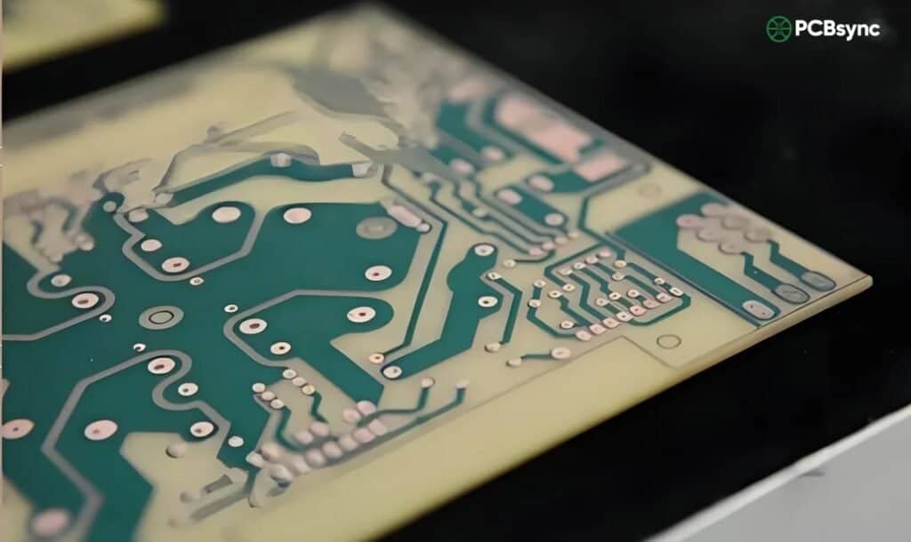
PCB etching is the process of selectively removing unwanted copper from a copper-clad laminate to create the conductive pathways (traces) that form your circuit. Think of it like sculpting—you start with a solid copper surface and carve away everything except the circuit pattern you need.
The etching process sits at the heart of PCB fabrication. Without it, there would be no way to transform your schematic designs into functional hardware. Every smartphone, computer, and electronic device contains boards that went through some form of etching during PCB manufacturing.
How PCB Etching Fits in the Manufacturing Process
The PCB manufacturing workflow follows a predictable sequence, and etching plays a critical role in the middle stages:
Stage
Process
Purpose
1
Design & Layout
Create circuit schematic and board layout
2
Substrate Preparation
Clean copper-clad laminate
3
Pattern Transfer
Apply resist layer to protect circuit traces
4
PCB Etching
Remove exposed copper chemically
5
Resist Removal
Strip protective mask from board
6
Drilling
Create holes for through-hole components
7
Finishing
Apply solder mask and surface finish
The etching stage determines whether your traces come out clean and precise or end up looking like a mess of broken lines and short circuits.
PCB Etching Methods: Finding What Works for Your Setup
Over the years, I’ve experimented with nearly every etching approach out there. Each method has its place depending on your budget, volume requirements, and precision needs.
Chemical Wet Etching
This is the traditional method that most hobbyists and small-scale manufacturers use. You immerse the masked PCB in a chemical solution that dissolves the exposed copper while leaving the protected areas intact.
Advantages:
Low equipment cost
Suitable for prototyping and small batches
Works well for standard trace widths (8 mil and above)
Limitations:
Isotropic etching causes undercutting
Chemical disposal requires proper handling
Results depend heavily on temperature and agitation control
Laser Etching
Laser etching uses high-powered laser beams to vaporize unwanted copper directly. No chemicals required—the laser literally burns away the copper you don’t need.
Advantages:
No chemical handling or disposal
Extremely precise for fine features
Maskless process (no resist application needed)
Limitations:
Equipment costs can exceed $10,000
Slower for large copper areas
May leave residue requiring post-processing
Plasma Etching (Dry Etching)
Plasma etching employs ionized gases in a vacuum chamber to remove material at the atomic level. This method appears primarily in high-end semiconductor and HDI board production.
Advantages:
Anisotropic etching (minimal undercutting)
Sub-25 μm feature resolution possible
Consistent results across large panels
Limitations:
Expensive equipment and maintenance
Requires vacuum chamber setup
Overkill for standard prototyping
Comparison Table: PCB Etching Methods
Method
Initial Cost
Feature Resolution
Speed
Best For
Chemical Wet
$50–200
8–12 mil
Moderate
DIY, prototyping
Laser
$5,000–50,000
3–6 mil
Slow for large areas
Rapid prototyping
Plasma
$20,000+
<2 mil
Fast
HDI production
CNC Milling
$500–5,000
6–10 mil
Moderate
Single boards
For most readers, chemical wet etching remains the practical choice. Let’s dive deeper into making it work reliably.
PCB Etching Chemicals: Choosing Your Etchant
The chemical you select for PCB etching affects everything from etch quality to safety considerations and disposal requirements. Here’s what I’ve learned from years of trial and error.
Ferric Chloride (FeCl₃)
Ferric chloride remains the most popular etchant among hobbyists and small manufacturers. It’s cheap, readily available, and gets the job done.
How it works: The ferric chloride reacts with metallic copper to form soluble copper chloride:
FeCl₃ + Cu → CuCl + FeCl₂
Pros:
Aggressive etching action
Long shelf life when stored properly
Works at room temperature (faster when heated to 40–50°C)
Cost-effective at around $15–20 per liter
Cons:
Dark brown color makes it impossible to see etching progress
Stains absolutely everything it touches
Cannot be regenerated easily
My tip: Always use ferric chloride in a plastic or glass container. It will destroy metal containers and permanently stain ceramic or porcelain.
Ammonium Persulfate
This has become my go-to etchant for precision work. The clear solution lets you watch the etching happen in real time.
Pros:
Transparent—you can monitor progress visually
Cleaner to work with than ferric chloride
No staining
Compatible with most resist inks
Cons:
Slower etching rate (20–30 minutes vs. 10–15 for ferric chloride)
More expensive per batch
Decomposes when heated above 50°C
Requires fresh mixing for each session
Best practice: Mix 250g of ammonium persulfate powder in 1 liter of warm water (around 40°C). Use immediately for best results.
Cupric Chloride (CuCl₂)
This is what professional shops often use because you can regenerate it indefinitely by bubbling air through the solution.
Pros:
Regenerable—lasts virtually forever with maintenance
If you want to avoid buying commercial chemicals, this kitchen-chemistry approach actually works surprisingly well.
Recipe:
1 part white vinegar (5% acetic acid)
1 part hydrogen peroxide (3% drugstore variety)
2 tablespoons table salt per cup of solution
Pros:
Made from household materials
Non-toxic and easy to dispose of
Great for beginners learning the process
Cons:
Slow (30–60 minutes per board)
Less consistent than commercial etchants
Salt must be replenished during etching
Chemical Comparison Summary
Etchant
Etch Time
Visibility
Cost
Disposal
Skill Level
Ferric Chloride
10–15 min
Poor
Low
Hazardous
Beginner
Ammonium Persulfate
20–30 min
Excellent
Medium
Hazardous
Beginner
Cupric Chloride
8–12 min
Good
Low (regenerable)
Hazardous
Intermediate
Vinegar/Peroxide
30–60 min
Excellent
Very Low
Safe
Beginner
The PCB Etching Process: Step-by-Step Guide
Now let’s get into the actual workflow. I’m going to walk you through this exactly as I do it in my workshop.
Step 1: Design Your PCB Layout
Start with proper PCB design software. Don’t try to hand-draw anything more complex than a simple test circuit.
Recommended free software:
KiCad (fully open source, professional-grade)
EasyEDA (browser-based, beginner-friendly)
Fritzing (good for Arduino-style projects)
Design rules for successful etching:
Minimum trace width: 10 mil (0.25 mm) for beginners
Minimum spacing: 10 mil between traces
Pad diameter: 1.5× the drill hole size
Add copper pour to reduce etching time
Export your design as a mirrored PDF or PNG at 600 DPI minimum. The mirror is critical—otherwise your final board will be backwards.
Step 2: Prepare the Copper-Clad Board
Surface preparation makes or breaks your etch results. I’ve ruined plenty of boards by skipping this step.
Cleaning procedure:
Cut your copper-clad board to size with a hacksaw or rotary tool
Sand the copper surface lightly with 400-grit sandpaper
Wash with dish soap and water
Rinse with distilled water
Wipe with isopropyl alcohol (90% or higher)
Let dry completely—do not touch the copper surface after cleaning
The copper should look uniformly bright with no oxidation spots or fingerprints.
Step 3: Transfer Your Design to the Board
This is where you create the protective mask that shields your traces from the etchant. Two main methods dominate the DIY world.
Toner Transfer Method
This uses a laser printer and heat to transfer toner directly onto the copper.
What you need:
Laser printer (inkjet won’t work)
Glossy paper or dedicated transfer paper (like Press-n-Peel Blue)
Clothes iron or laminator
Process:
Print your mirrored design on glossy paper using maximum toner density
Place the printed side face-down on the clean copper
Apply heat with an iron on linen setting for 3–5 minutes
Press firmly and move the iron slowly across the entire surface
Soak the board in warm water for 5 minutes
Peel away the paper carefully
Touch up any gaps with a permanent marker (Sharpie works fine)
Common problems:
Patchy transfer: Iron temperature too low or pressure uneven
Toner smearing: Iron too hot or moved too quickly
Paper sticking: Didn’t soak long enough
Photoresist Method
This produces more consistent results, especially for fine-pitch designs.
What you need:
Presensitized PCB or dry film photoresist
Transparency film for printing
UV light source (nail curing lamp works)
Developer solution (sodium carbonate)
Process:
Print your design on transparency film (use two layers for better UV blocking)
Place transparency on photoresist-coated board
Expose to UV light for 2–4 minutes (timing varies by light source)
Develop in sodium carbonate solution until pattern appears
Rinse with water
The photoresist method produces sharper edges and works better for traces below 10 mil.
Step 4: Etch the Board
Now the actual etching happens. This part requires patience and attention.
Setup:
Pour etchant into a plastic container (deep enough to cover the board)
Heat etchant to 40–50°C if using ferric chloride (optional but speeds up the process)
Place the board in the solution with the copper side facing up
During etching:
Agitate the solution constantly by rocking the container or using aquarium air bubbles
Check progress every 2–3 minutes
Remove the board as soon as all exposed copper disappears
Critical timing: Over-etching destroys your traces. Under-etching leaves copper bridges that short your circuits. Watch carefully and pull the board the moment the last bit of exposed copper dissolves.
For a standard 1 oz copper board with ferric chloride at 45°C, expect 8–12 minutes.
Step 5: Clean and Inspect
Once etching is complete:
Rinse the board immediately under running water for 30 seconds
Remove the toner or photoresist with acetone
Dry the board with a lint-free cloth
Inspect under good lighting with a magnifying glass
What to look for:
Broken traces (need bridging with wire or starting over)
Copper bridges between traces (can sometimes be scraped away with a knife)
Pitting or thin spots (may cause reliability issues)
Step 6: Drill and Finish
The etching is done, but your board needs a few more steps before it’s ready.
Drilling:
Use carbide micro drill bits (HSS dulls quickly on fiberglass)
Standard via holes: 0.8 mm
Component leads: 0.9–1.0 mm
Use a drill press or Dremel in a stand for accuracy
Finishing options:
Tin plating prevents oxidation and improves solderability
Solder mask (apply with spray or photoresist) protects traces
Silkscreen adds component references (optional for prototypes)
Troubleshooting Common PCB Etching Problems
After etching hundreds of boards, I’ve encountered every possible failure mode. Here’s how to diagnose and fix the most common issues.
Under-Etching
Symptoms: Copper remains in areas that should be clear, causing shorts between traces.
Causes:
Etchant too weak or exhausted
Temperature too low
Insufficient agitation
Etching time too short
Solutions:
Use fresh etchant
Heat to 40–50°C
Agitate continuously
Extend etching time in 2-minute increments
Over-Etching
Symptoms: Traces are thinner than designed, some may be broken or completely dissolved.
Causes:
Etching time too long
Etchant too aggressive (temperature too high)
Weak resist adhesion
Thin resist coating
Solutions:
Monitor closely and remove board immediately when clear
Reduce etchant temperature
Improve surface cleaning before resist application
Apply thicker resist layer or use better transfer paper
Undercutting
Symptoms: Traces have narrowed base (trapezoidal cross-section), edges look rough.
Causes:
Isotropic nature of wet chemical etching
Poor resist adhesion at edges
Extended etch time
Solutions:
Use alkaline etchant instead of acid-based
Improve resist adhesion through better surface prep
Minimize etch time by using fresh, heated etchant
Uneven Etching
Symptoms: Some areas etch faster than others, leaving copper islands or thin spots.
Causes:
Uneven etchant distribution
Inconsistent resist thickness
Board not level in solution
Solutions:
Agitate constantly and rotate board during etching
Apply resist evenly during transfer
Ensure board floats copper-side-down or use vertical immersion
Troubleshooting Quick Reference
Problem
Most Likely Cause
First Fix to Try
Copper won’t etch
Exhausted etchant
Use fresh solution
Traces broken
Over-etching
Reduce time/temperature
Rough edges
Poor resist adhesion
Better surface cleaning
Uneven results
No agitation
Rock container constantly
Resist lifting
Contaminated copper
Clean with alcohol before transfer
Safety Precautions for PCB Etching
I can’t stress this enough: PCB etching chemicals are hazardous. I’ve had a few close calls over the years, and proper safety gear has saved me every time.
Personal Protective Equipment
Always wear:
Chemical-resistant gloves (nitrile or neoprene)
Safety glasses or goggles
Long sleeves and closed-toe shoes
Apron for splash protection
Ventilation Requirements
All etching should happen in well-ventilated areas. Ferric chloride produces mild fumes, but ammonium persulfate and cupric chloride can release irritating gases, especially when heated.
Minimum setup:
Work near an open window with fan
Better: Use a fume hood or outdoor workspace
Chemical Disposal
Never pour etchant down the drain. These chemicals contain dissolved copper and other metals that damage plumbing and pollute waterways.
Proper disposal options:
Take to household hazardous waste collection
Neutralize and precipitate copper (for cupric chloride)
Contact local waste management for guidance
Neutralization process for ferric chloride:
Add sodium carbonate (washing soda) until pH reaches 7
Let copper hydroxide precipitate
Filter and dispose of solid as hazardous waste
Liquid can then be disposed of safely
DIY PCB Etching at Home: Practical Tips
For those setting up a home etching station, here’s what I’ve learned about making the process work reliably without breaking the bank.
Budget Setup Essentials
Item
Purpose
Approximate Cost
Copper-clad board (10 pack)
Raw material
$15–25
Ferric chloride (1L)
Etchant
$15–20
Laser printer paper (glossy)
Toner transfer
$10
Plastic container with lid
Etching tank
$5
Nitrile gloves (box)
Protection
$10
Isopropyl alcohol (1L)
Cleaning
$5
400-grit sandpaper
Surface prep
$3
Permanent marker
Touch-ups
$3
Total
$66–96
Tips for Consistent Results
Keep a log. Record etchant temperature, time, and results for each board. You’ll quickly identify what works for your specific setup.
Standardize your process. Use the same paper, iron temperature, and cleaning procedure every time. Variables are the enemy of consistency.
Fresh etchant matters. Don’t try to stretch old etchant too far. If ferric chloride turns dark green, it’s exhausted.
Temperature control. A simple aquarium heater in a water bath keeps etchant at the optimal temperature with no babysitting.
Agitation is key. I use an aquarium air pump with a bubble stone. It provides constant, even agitation without manual effort.
Useful Resources for PCB Design and Etching
Here are the tools and references I actually use regularly.
Free PCB Design Software
Software
Platform
Best For
Download Link
KiCad
Windows, Mac, Linux
Professional-grade designs
kicad.org/download
EasyEDA
Browser-based
Quick prototypes
easyeda.com
Fritzing
Windows, Mac, Linux
Arduino projects
fritzing.org
Component Libraries and Footprints
SnapMagic Search (snapeda.com) – Free footprints for most CAD software
Ultra Librarian – Manufacturer-verified component data
KiCad Official Libraries – Included with software
PCB Fabrication Services
When you need boards faster or more precise than DIY allows:
Service
Turnaround
Minimum Order
Notes
JLCPCB
1–2 days + shipping
5 boards
Incredibly cheap for prototypes
PCBWay
1–3 days + shipping
5 boards
Good quality, assembly available
OSH Park
2–3 weeks
3 boards
Purple boards, US-based
Educational Resources
Hackaday articles on PCB fabrication techniques
YouTube channels: GreatScott!, EEVblog, Ben Eater
Electronics Stack Exchange for troubleshooting questions
When to DIY vs. When to Order
After all this, you might wonder when home etching makes sense versus ordering from a fabrication house.
DIY makes sense when:
You need one board today
You’re learning the process
Design changes frequently during prototyping
Board is simple (single layer, large traces)
Order from a fab when:
You need more than 5 identical boards
Design requires 2+ layers
Traces are below 8 mil
You need solder mask and silkscreen
Time isn’t critical (a week turnaround is acceptable)
At current prices ($2 for 5 boards from some Chinese fabs), the economic argument for DIY etching only works for single, urgent prototypes. But the skills you develop transfer directly to understanding what’s possible in your designs.
Frequently Asked Questions
What chemicals are used for PCB etching?
The most common chemicals for PCB etching are ferric chloride, ammonium persulfate, and cupric chloride. Ferric chloride is the most widely available and works at room temperature, making it popular with hobbyists. Ammonium persulfate offers a cleaner workspace since it’s transparent, but it works more slowly. For a completely non-toxic alternative, a mixture of white vinegar, hydrogen peroxide, and salt can etch copper, though it takes 30–60 minutes per board.
How long does PCB etching take?
Etching time depends on your chemical choice and temperature. Ferric chloride at 45°C etches a standard 1 oz copper board in 8–12 minutes. Ammonium persulfate takes 15–25 minutes at 40°C. The DIY vinegar-peroxide mixture needs 30–60 minutes. Thicker copper (2 oz) roughly doubles these times. Always watch the board rather than the clock—remove it immediately when the last exposed copper disappears.
Can I etch PCBs at home safely?
Yes, with proper precautions. Always wear chemical-resistant gloves and safety glasses. Work in a well-ventilated area or outdoors. Keep etchant away from children and pets. Never mix different chemicals together. Have baking soda on hand to neutralize spills. Store chemicals in labeled, sealed containers. Dispose of used etchant through hazardous waste collection, never down the drain.
What is the difference between toner transfer and photoresist methods?
Toner transfer uses a laser printer and heat to transfer toner directly onto copper, creating the etch resist. It’s cheaper and requires less equipment but can produce inconsistent results, especially for fine traces below 10 mil. Photoresist uses UV-sensitive film or spray that hardens when exposed to UV light through a transparency mask. It produces sharper, more consistent results and works better for complex designs, but requires additional equipment (UV light source) and chemicals (developer solution).
What’s the minimum trace width I can achieve with DIY etching?
With careful technique, home etching can reliably produce 8 mil (0.2 mm) traces using the toner transfer method and 6 mil (0.15 mm) with photoresist. Achieving finer features requires expensive equipment (laser etching) or ordering from professional fabricators. For beginners, I recommend starting with 12 mil traces and working down as your skills improve. Most through-hole component designs work fine with 10–12 mil traces.
Advanced PCB Etching Techniques
Once you’ve mastered the basics, several advanced techniques can improve your results significantly.
Double-Sided Board Etching
Creating double-sided PCBs at home is challenging but possible. The key difficulty lies in aligning the top and bottom patterns precisely.
Alignment methods:
Registration holes method:
Drill alignment holes in the corners before any pattern transfer
Print both layers with corresponding alignment marks
Use pins through the holes to align transparencies during exposure
Etch one side, then flip and etch the other
Sandwich method:
Align both transparencies together against a light source
Tape or staple edges together
Insert the copper board between them
Transfer or expose both sides simultaneously
For through-hole connections between layers, you’ll need to drill vias and fill them with wire or solder. This process requires patience but yields functional two-layer boards.
Achieving Finer Traces
Pushing the limits of DIY etching requires attention to several factors:
Surface preparation improvements:
Use brass wool instead of sandpaper for a smoother finish
Apply an oxide conversion coating (phosphoric acid based)
Consider electropolishing for ultimate surface quality
Transfer optimization:
Use dedicated transfer papers (Press-n-Peel, Pulsar)
Overlay two printed transparencies for photoresist method
Lower laminator temperature slightly for thinner traces
Etching refinements:
Use vertical immersion to prevent etchant pooling
Lower etchant concentration for slower, more controlled removal
Add surfactant (tiny amount of dish soap) for more even etching
Temperature Control Systems
Consistent temperature dramatically improves etch results. Here’s my setup for maintaining optimal conditions:
Water bath method:
Place etchant container inside a larger container of water
Use an aquarium heater set to 45°C in the water bath
The water transfers heat evenly to the etchant
Add a thermometer to monitor actual etchant temperature
Active temperature control:
PID-controlled heating elements maintain precise temperatures
Some hobbyists use sous vide cookers as heat sources
Target 40–50°C for ferric chloride, 35–45°C for ammonium persulfate
Etchant Regeneration
For cupric chloride solutions, regeneration extends etchant life indefinitely:
Regeneration process:
Bubble air through the solution using an aquarium pump
Add small amounts of hydrochloric acid as needed
Monitor solution color (should remain dark green)
Remove copper buildup periodically
This approach reduces chemical waste and long-term costs significantly. Professional shops use this technique to maintain consistent etch rates across thousands of boards.
Industry Trends in PCB Etching
The PCB industry continues evolving, with several trends affecting how boards get manufactured.
Eco-Friendly Etchants
Environmental regulations are driving development of greener etching solutions. Newer formulations include:
Biodegradable copper etchants with reduced toxicity
Closed-loop systems that recover and recycle copper
While not yet common in hobby applications, these alternatives are becoming more accessible.
Additive vs. Subtractive Manufacturing
Traditional PCB etching is subtractive—you start with copper everywhere and remove what you don’t need. Additive manufacturing (depositing copper only where needed) is gaining traction for certain applications.
Additive advantages:
Less material waste
Potentially finer features
Enables 3D printed electronics integration
Current limitations:
Higher equipment costs
Slower for large copper areas
Conductivity may not match bulk copper
For most practical purposes, subtractive etching remains the dominant approach, but additive techniques appear in specialized applications like flexible electronics and embedded components.
AI-Optimized Etching Parameters
Manufacturing facilities increasingly use machine learning to optimize etching parameters in real time. Sensors monitor etchant chemistry, temperature, and spray pressure, while algorithms adjust conditions dynamically.
For DIY applications, the lesson is clear: consistent process monitoring improves results. Even simple logging of your parameters helps identify what works best for your setup.
Comparing DIY Etching to Professional Fabrication
Understanding the differences helps you decide when each approach makes sense.
For very small quantities (1–3 boards), DIY can be cheaper if you already own the equipment. However, professional fabrication costs have dropped dramatically:
JLCPCB: 5 boards for approximately $2–5 + shipping
PCBWay: Similar pricing with more options
OSH Park: Higher quality at $5/square inch
When you factor in your time, materials, and the occasional failed board, ordering often makes economic sense for anything beyond immediate, single-board needs.
Time Comparison
DIY timeline:
Design: Variable
Material prep: 15 minutes
Pattern transfer: 30–60 minutes
Etching: 15–30 minutes
Cleanup and drilling: 30–60 minutes
Total: 2–4 hours per board
Professional fab timeline:
Design: Variable
Order placement: 10 minutes
Fabrication: 1–3 days
Shipping: 1–14 days depending on location
Total: 3–17 days, but minimal active time
DIY wins when you need something today. Professional fab wins when you’re planning ahead.
Common Mistakes I Made (So You Don’t Have To)
Learning PCB etching involved plenty of failures. Here are lessons from my worst mistakes:
Mistake 1: Insufficient Cleaning
My first dozen boards had spotty transfer because I thought wiping with a paper towel was enough. Fingerprint oils and oxidation are invisible but absolutely destroy resist adhesion.
Solution: Always sand, wash, alcohol wipe, and never touch the copper after cleaning.
Mistake 2: Impatience During Transfer
I used to peel the transfer paper immediately after ironing. The toner hadn’t bonded properly and came right off.
Solution: Let the board cool to room temperature before peeling. Better yet, soak in warm water for 5 minutes to dissolve the paper’s adhesive.
Mistake 3: Checking Progress Too Often
Constantly pulling the board out of etchant extends total etch time and creates uneven results. Each removal lets the etchant drain unevenly.
Solution: Trust your timing. Check at 60% of expected time, then watch through the solution if using ammonium persulfate.
Mistake 4: Wrong Copper Thickness Expectations
I once ordered 2 oz copper boards thinking “more is better” for power traces. They took forever to etch and undercut badly.
Solution: Use 1 oz copper for most applications. 2 oz copper requires adjusted etch parameters and longer times.
Mistake 5: No Test Patterns
Jumping straight into complex boards meant debugging both my process AND my design simultaneously.
Solution: Create a test pattern with various trace widths. Use it to dial in your process before committing to real designs.
Wrapping Up
PCB etching transforms your circuit designs from screen to reality. While the process involves hazardous chemicals and requires attention to detail, the fundamentals are straightforward once you understand them.
Start with the toner transfer method and ferric chloride—they’re forgiving of beginner mistakes and produce acceptable results for most prototype work. As your skills develop, experiment with photoresist for finer features and ammonium persulfate for cleaner operation.
The boards you etch yourself might not match the precision of commercial fabricators, but there’s something deeply satisfying about holding a circuit board you created from start to finish. That tangible connection to your electronics projects makes the learning curve worthwhile.
Inquire: Call 0086-755-23203480, or reach out via the form below/your sales contact to discuss our design, manufacturing, and assembly capabilities.
Quote: Email your PCB files to Sales@pcbsync.com (Preferred for large files) or submit online. We will contact you promptly. Please ensure your email is correct.
Notes: For PCB fabrication, we require PCB design file in Gerber RS-274X format (most preferred), *.PCB/DDB (Protel, inform your program version) format or *.BRD (Eagle) format. For PCB assembly, we require PCB design file in above mentioned format, drilling file and BOM. Click to download BOM template To avoid file missing, please include all files into one folder and compress it into .zip or .rar format.


