Inquire: Call 0086-755-23203480, or reach out via the form below/your sales contact to discuss our design, manufacturing, and assembly capabilities.
Quote: Email your PCB files to Sales@pcbsync.com (Preferred for large files) or submit online. We will contact you promptly. Please ensure your email is correct.
Notes: For PCB fabrication, we require PCB design file in Gerber RS-274X format (most preferred), *.PCB/DDB (Protel, inform your program version) format or *.BRD (Eagle) format. For PCB assembly, we require PCB design file in above mentioned format, drilling file and BOM. Click to download BOM template To avoid file missing, please include all files into one folder and compress it into .zip or .rar format.
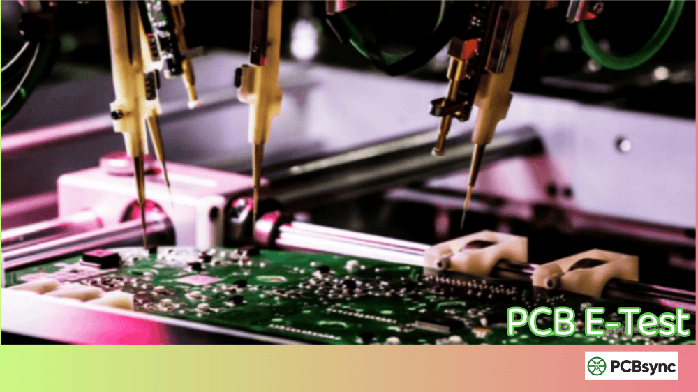
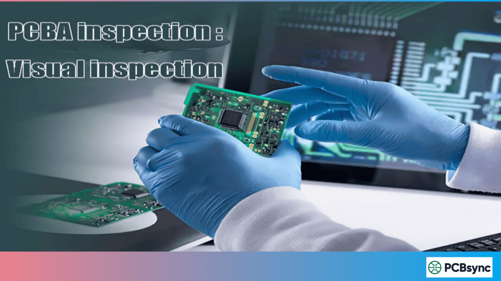
E-Test (Electrical Test) is the final quality gate that every bare PCB must pass before it leaves the factory. As someone who has spent years on the manufacturing floor, I can tell you that skipping or underestimating this step is the fastest way to turn a good design into an expensive pile of scrap. In this guide, I’ll walk you through everything you need to know about PCB E-Test—from the basic principles to advanced testing methods—so you can make informed decisions for your next project.
Whether you’re ordering prototypes or scaling up to mass production, understanding E-Test will help you communicate better with your PCB supplier, reduce defect rates, and ultimately save money.
E-Test, short for Electrical Test, is a verification process performed on bare (unpopulated) printed circuit boards to confirm that all electrical connections match the original design intent. The test checks two critical aspects:
Continuity Testing (Opens Detection): Verifies that all nets that should be connected are actually connected. An “open” occurs when a trace, via, or connection that should conduct electricity is broken or missing.
Isolation Testing (Shorts Detection): Confirms that nets that should remain separate are not accidentally connected. A “short” happens when two unrelated conductors are electrically bridged—often due to copper residue, solder mask issues, or etching defects.
This testing follows the IPC-9252 standard, which defines the guidelines and requirements for electrical testing of unpopulated printed boards. The test equipment applies voltage signals through probes and measures resistance values to determine pass/fail status.
Why E-Test Matters More Than Ever
Back when PCBs had larger traces and fewer layers, visual inspection could catch most defects. Those days are gone. Modern boards feature:
Blind and buried vias invisible from the surface
HDI (High-Density Interconnect) designs with 3mil traces
20+ layer stackups with complex interconnections
BGA escape routing that’s impossible to inspect visually
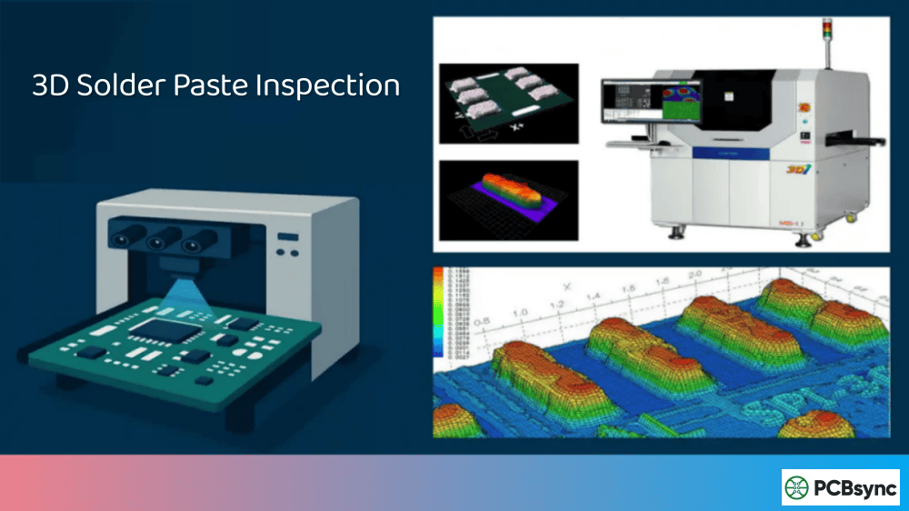
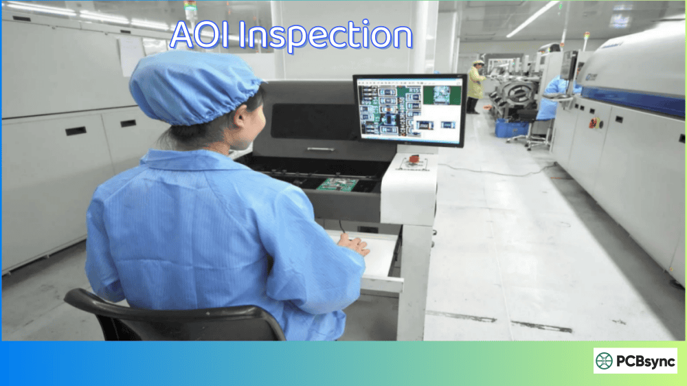
Only E-Test can verify that a 0.1mm via buried on layer 4 actually connects to layer 8 as designed. AOI (Automated Optical Inspection) sees the surface—E-Test sees the electrical reality.
E-Test Methods: Flying Probe vs. Fixture Testing
There are two primary methods for conducting E-Test, and choosing the right one depends on your production volume, budget, and timeline.
Flying Probe Testing
Flying probe testing uses motorized probes (typically 4-8 heads) that move across the PCB surface, making contact with test points in sequence. The probes “fly” from point to point based on a software-controlled program generated from your netlist data.
How It Works:
The PCB is loaded and secured on the test platform
Probes move to designated test points (pads, vias, component locations)
Continuity and isolation measurements are performed sequentially
Results are logged and compared against the netlist
Best For:
Prototypes and engineering samples
Low-to-medium volume production (typically under 500 boards)
Designs with frequent revisions
Complex HDI boards with limited test access
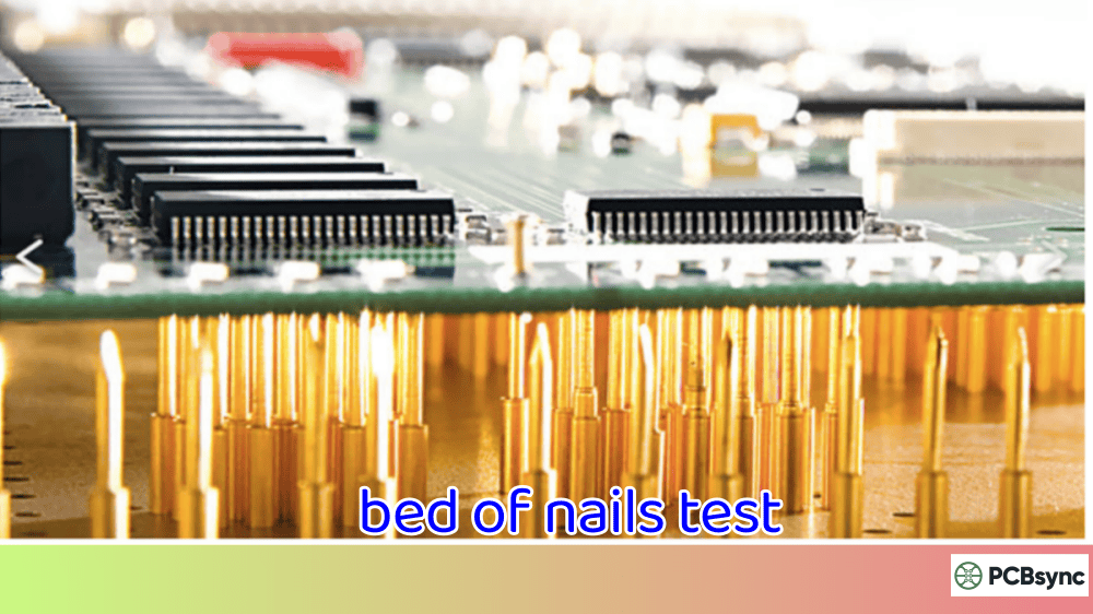
Fixture Testing (Bed of Nails)
Fixture testing uses a custom-built test fixture containing hundreds or thousands of spring-loaded “pogo pins” that align with test points on your PCB. When the board is pressed against the fixture, all test points make simultaneous contact, allowing rapid parallel testing.
How It Works:
A custom fixture is designed and manufactured for your specific PCB layout
The PCB is placed on the fixture
All test points are probed simultaneously
Complete electrical verification happens in seconds
Best For:
High-volume production runs (1000+ boards)
Stable designs with minimal revisions expected
Applications requiring fastest possible throughput
Flying Probe vs. Fixture: Quick Comparison
Factor
Flying Probe
Fixture (Bed of Nails)
Setup Cost
None (no fixture required)
$500–$20,000+ per fixture
Setup Time
Hours (program generation)
Days to weeks
Test Speed
1–5 minutes per board
5–30 seconds per board
Flexibility
High (easy design changes)
Low (new fixture for changes)
Minimum Pitch
0.1mm (4mil)
0.5mm (20mil) typical
Best Volume
1–500 units
500+ units
Cost per Board
Higher for large volumes
Lower for large volumes
Pro Tip: Many manufacturers offer a hybrid approach—flying probe for initial qualification and low volumes, then transitioning to fixture testing when production stabilizes.
Your PCB manufacturer needs accurate data to create E-Test programs. The IPC-D-356 format (also called IPC-356) is the industry-standard netlist format specifically designed for electrical testing.
What the IPC-D-356 File Contains
The IPC-D-356 is an ASCII text file that includes:
Net names: Identifier for each electrical network
Test point coordinates: X/Y locations for probing
Pin assignments: Component reference designators
Access information: Which layer(s) can be probed
Hole/via data: Through-hole and via locations
Why You Should Always Provide Your Own Netlist
When you supply an IPC-D-356 netlist exported directly from your CAD tool (Altium, KiCad, OrCAD, etc.), your manufacturer can:
Verify Gerber accuracy before production starts
Detect CAM errors during file processing
Ensure 100% test coverage based on your design intent
If you don’t supply a netlist, the manufacturer will extract one from your Gerbers. This works, but it’s only as good as the Gerber data itself—any errors in your output files will propagate into the test program.
How to Export IPC-D-356 from Common CAD Tools
CAD Tool
Export Path
Altium Designer
File → Fabrication Outputs → Test Point Report → Enable IPC-D-356A
The IPC-9252 standard defines different testing levels based on the end-use application of your PCB. Understanding these classes helps you communicate requirements to your manufacturer.
IPC Testing Classes Overview
Class
Application
Continuity Threshold
Isolation Voltage
Typical Use Cases
Class 1
General Electronics
≤50Ω
≥40VDC
Consumer products, toys
Class 2
Dedicated Service
≤20Ω
≥100VDC
Industrial, telecom
Class 3
High Reliability
≤10Ω
≥250VDC
Medical, military, aerospace
Class 3/A
Aerospace/Military Avionics
≤10Ω
≥250VDC, 100MΩ insulation
Flight-critical systems
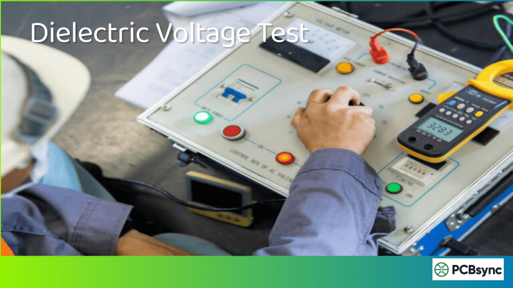
Key Insight: Higher voltage during isolation testing helps detect marginal shorts and contamination that lower voltages might miss. If you’re building safety-critical products, don’t settle for Class 1 testing parameters.
What Gets Tested During E-Test
Test Type
What It Checks
Pass Criteria
Opens Test
Current flow between nodes in the same net
Resistance below threshold (e.g., <10Ω)
Shorts Test
Isolation between different nets
Resistance above threshold (e.g., >20MΩ)
100% Netlist Test
Every node on every net
Complete verification
Optimized Netlist
End-of-net points + selected midpoints
Faster but less comprehensive
Hi-Pot Test
High voltage insulation integrity
No breakdown at specified voltage
4-Wire Kelvin
Precise low-resistance measurement
Accurate milli-ohm readings
The E-Test Process Flow: What Happens at the Factory
Understanding the E-Test workflow helps you appreciate why proper documentation matters and what to expect from your manufacturer.
Step 1: Test Program Generation
Before any probing happens, the test system needs instructions. The manufacturer’s CAM team:
Imports your netlist (IPC-D-356 or Gerber-extracted)
Identifies all test points including pads, vias, and component locations
Optimizes the probe path for flying probe efficiency
Sets test parameters based on your IPC class requirements
Validates the program against your design data
This step typically takes 1-4 hours for flying probe (automated) or 2-5 days for fixture design (manual engineering work).
Step 2: First Article Testing
The first boards off the production line receive extra scrutiny:
Complete 100% netlist verification
Detailed failure analysis if any issues found
Comparison against original design intent
Documentation for traceability
First article inspection (FAI) results should be reviewed before approving mass production.
Step 3: Production Testing
During production runs, every board passes through E-Test:
Flying Probe: Boards tested one at a time, full verification
Fixture: Multiple boards tested simultaneously (if panel fixtures are used)
Real-time logging: Test results recorded for quality tracking
Automatic rejection: Failed boards are marked and segregated
Step 4: Failure Analysis and Reporting
When boards fail E-Test, the test system provides detailed diagnostic data:
Specific net names with opens or shorts
Physical coordinates of the fault location
Resistance measurements at failure points
Visual maps showing problem areas
Good manufacturers share this data with you, especially for first articles or when investigating yield issues.
Common Defects Detected by E-Test
E-Test catches manufacturing defects that would otherwise make your boards non-functional. Here’s what the test reveals:
Open Circuit Causes
Incomplete trace etching
Drilling misalignment (via doesn’t contact pad)
Broken internal traces in multilayer boards
Contamination preventing plating adhesion
Cracked annular rings
Short Circuit Causes
Copper residue between traces (insufficient etching)
Solder mask misregistration
Bridging in fine-pitch areas
Internal layer alignment issues
CAM errors during panelization
Real-World Example
I recently worked on a 12-layer HDI board where visual inspection and AOI passed every panel. E-Test caught that 3% of boards had opens in buried vias on layers 5-6—something completely invisible from the surface. Without E-Test, those boards would have gone to assembly, wasted components, and delayed the project by weeks.
Best Practices for Design for Testability (DFT)
Good design practices make E-Test more reliable and cost-effective. Here’s what I recommend:
Test Point Placement Guidelines
Add dedicated test pads on critical nets when possible
Avoid placing test points under components that obstruct probe access
Maintain minimum 0.5mm spacing between adjacent test points for fixture compatibility
Place test points on a grid when targeting fixture testing
Ensure via-in-pad designs have clear access points elsewhere on the net
Netlist Hygiene
Clean up your netlist before export—remove unnamed nets if not intentional
Document intentional shorts (like fused jumpers) so they’re not flagged as failures
Include power/ground planes in your netlist for comprehensive testing
When to Request 100% E-Test
Always request 100% E-Test for:
First article inspection (FAI)
Medical, aerospace, or automotive applications
High-layer-count boards (8+ layers)
Any design with blind/buried vias
Production qualification runs
Useful Resources and Downloads
Here are essential documents and tools for PCB electrical testing:
IPC Standards (Available from IPC.org)
IPC-9252B – Requirements for Electrical Testing of Unpopulated Printed Boards
IPC-6012 – Qualification and Performance Specification for Rigid Printed Boards
IPC-D-356B – Bare Substrate Electrical Test Data Format
Free Tools and References
Resource
Description
Link
IPC-D-356 Format Guide
Simplified format explanation
downstreamtech.com
Altium Netlist Export Tutorial
Step-by-step IPC-356 export
altium.com/documentation
KiCad IPC Netlist
Official KiCad documentation
docs.kicad.org
Manufacturer E-Test Capabilities
When evaluating PCB suppliers, ask these questions:
What E-Test methods do you offer? (Flying probe, fixture, both)
What is your minimum test pitch capability?
Do you perform 100% E-Test on all boards or sample testing?
Can you test to IPC-9252 Class 3 requirements?
Do you provide E-Test reports or certificates of conformance?
Frequently Asked Questions About PCB E-Test
What is the difference between E-Test and ICT?
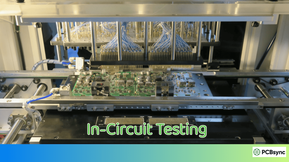
E-Test (Electrical Test) is performed on bare boards before assembly and verifies connectivity/isolation of the copper networks. ICT (In-Circuit Test) is performed on assembled boards and tests component values, orientation, and functionality. E-Test catches PCB manufacturing defects; ICT catches assembly defects.
How much does E-Test cost?
Most PCB manufacturers include basic E-Test in their standard pricing. Flying probe testing is typically free or low-cost for small quantities. Fixture-based testing involves a one-time fixture charge ($500–$20,000 depending on complexity) but lower per-board costs at volume. Always clarify testing scope in your quote.
Can E-Test detect all PCB defects?
No. E-Test verifies electrical connectivity only. It cannot detect:
Combine E-Test with AOI and mechanical inspection for comprehensive quality control.
Is E-Test necessary for prototype boards?
Absolutely. Prototypes often have design errors that need debugging. Knowing your bare boards are electrically correct before PCB assembly eliminates one major variable. When your prototype doesn’t work, you’ll know the problem is in your design or assembly—not the PCB fabrication.
What does “100% E-Test” actually mean?
100% E-Test means every single board in your order is electrically tested—not just samples. Every net is verified for continuity, and isolation is checked between all adjacent and non-adjacent nets. This is the standard practice at reputable manufacturers and should be your default expectation.
Troubleshooting E-Test Failures
When your boards fail E-Test, don’t panic. Most issues fall into predictable categories with straightforward solutions.
Analyzing Open Circuit Failures
When the test report shows opens, investigate these root causes:
Symptom
Likely Cause
Solution
Opens on multiple vias
Drilling registration error
Review drill-to-copper alignment tolerances
Opens on fine traces
Under-etching or over-etching
Check etching process parameters
Opens on inner layers
Lamination void or contamination
Request cross-section analysis
Random opens across board
Plating adhesion failure
Investigate surface preparation process
Analyzing Short Circuit Failures
Shorts are often easier to diagnose because they frequently appear in patterns:
Symptom
Likely Cause
Solution
Shorts between adjacent traces
Insufficient etching
Reduce trace spacing or optimize etching
Shorts on power/ground planes
Inner layer misregistration
Review layer alignment tolerances
Random shorts
Copper contamination
Improve cleaning and inspection
Shorts after solder mask
Mask registration or thickness
Check solder mask process
Working with Your Manufacturer
When you receive E-Test failure reports, request:
Failure maps showing physical locations of defects
Root cause analysis for systematic failures (>1% defect rate)
Corrective action plans for recurring issues
Process capability data (Cpk) for critical features
A good manufacturer treats E-Test data as a process improvement tool, not just a pass/fail gate.
E-Test Equipment: Understanding the Technology
Modern E-Test equipment has evolved significantly. Understanding what your manufacturer uses helps you set realistic expectations.
Flying Probe Tester Specifications
High-end flying probe testers feature:
4-8 independent probe heads (some advanced systems have 16+)
0.1mm minimum pitch capability
±10μm positioning accuracy
Automated camera systems for component verification
Kelvin 4-wire measurement for milliohm precision
Test time varies from 30 seconds (simple 2-layer boards) to 10+ minutes (complex multilayer HDI).
Fixture Tester Specifications
Bed-of-nails fixtures and testers typically offer:
Simultaneous testing of thousands of points
Test cycle time of 5-30 seconds per board
0.5mm minimum pitch for standard fixtures
Vacuum or mechanical clamping for board contact
High-volume throughput of 100+ boards per hour
The fixture cost scales with board complexity and test point count—expect $1,000-$5,000 for typical boards, up to $20,000+ for high-density designs.
Conclusion: Making E-Test Work for You
E-Test is more than a checkbox on your manufacturing spec—it’s your assurance that months of design work won’t be wasted on electrically defective boards. Here’s my advice after years of dealing with PCB quality issues:
For Prototypes: Always request 100% E-Test with flying probe. It adds minimal cost and catches problems before expensive assembly.
For Production: Work with your manufacturer to determine the break-even point between flying probe and fixture testing. Often, 300-500 boards is the crossover point.
For Critical Applications: Specify IPC-9252 Class 3 testing parameters and request test documentation. Don’t assume—verify.
The best PCB is one that works the first time. Proper E-Test makes that happen.
Inquire: Call 0086-755-23203480, or reach out via the form below/your sales contact to discuss our design, manufacturing, and assembly capabilities.
Quote: Email your PCB files to Sales@pcbsync.com (Preferred for large files) or submit online. We will contact you promptly. Please ensure your email is correct.
Notes: For PCB fabrication, we require PCB design file in Gerber RS-274X format (most preferred), *.PCB/DDB (Protel, inform your program version) format or *.BRD (Eagle) format. For PCB assembly, we require PCB design file in above mentioned format, drilling file and BOM. Click to download BOM template To avoid file missing, please include all files into one folder and compress it into .zip or .rar format.


