Inquire: Call 0086-755-23203480, or reach out via the form below/your sales contact to discuss our design, manufacturing, and assembly capabilities.
Quote: Email your PCB files to Sales@pcbsync.com (Preferred for large files) or submit online. We will contact you promptly. Please ensure your email is correct.
Notes: For PCB fabrication, we require PCB design file in Gerber RS-274X format (most preferred), *.PCB/DDB (Protel, inform your program version) format or *.BRD (Eagle) format. For PCB assembly, we require PCB design file in above mentioned format, drilling file and BOM. Click to download BOM template To avoid file missing, please include all files into one folder and compress it into .zip or .rar format.
If you’ve ever struggled with toner transfer methods or dealt with inconsistent results using liquid photoresist, you know how frustrating PCB fabrication can be. After 15 years of working in PCB manufacturing and countless hours spent troubleshooting image transfer issues, I can tell you that switching to PCB dry film was a game-changer for my workflow.
PCB dry film photoresist has become the industry standard for transferring circuit patterns onto copper-clad boards. Whether you’re prototyping at home or running a production line, understanding how to properly use dry film will dramatically improve your circuit board quality.
In this guide, I’ll walk you through everything you need to know about PCB dry film—from selecting the right thickness to troubleshooting common problems that I’ve encountered over the years. Let’s get your boards looking professional.
PCB dry film is a photosensitive polymer material that comes in a three-layer sandwich structure. Unlike liquid photoresist that you brush or spray on, dry film arrives as a solid sheet that you laminate directly onto your copper-clad board using heat and pressure.
The structure consists of:
Top layer (Mylar/Polyester film): Acts as a protective cover and oxygen barrier during exposure
Middle layer (Photopolymer): The actual photosensitive material that reacts to UV light
Bottom layer (Polyethylene film): A separator that you remove before lamination
When UV light hits the exposed areas of negative-type dry film (the most common type), those areas undergo polymerization and harden. The unexposed areas remain soft and wash away during development, leaving you with precise circuit patterns.
PCB Dry Film vs. Other Image Transfer Methods
I’ve tried every method out there—toner transfer, spray photoresist, even hand-painting with etch resist pens. Here’s how dry film stacks up:
Method
Resolution
Consistency
Ease of Use
Cost per Board
PCB Dry Film
50µm (excellent)
High
Medium
Low-Medium
Toner Transfer
200µm (fair)
Low
Easy
Very Low
Liquid Photoresist
75µm (good)
Medium
Difficult
Medium
Direct Laser
100µm (good)
High
Easy (expensive equipment)
High
The main advantages that sold me on dry film were the consistent thickness across the entire board and the ability to achieve fine traces down to 50µm line/space. When you’re working with QFN or TSSOP packages, that precision matters.
Choosing the Right PCB Dry Film Thickness
Selecting the correct film thickness is one of the most overlooked aspects of the process. Most hobbyists grab whatever’s cheapest on eBay without considering how thickness affects their results.
Dry Film Thickness Selection Guide
Thickness
Best Applications
Resolution Capability
Notes
0.5 mil (15µm)
Ultra-fine line HDI
< 25µm L/S
Professional use only
0.8 mil (20µm)
Fine pitch SMD, flex boards
25-50µm L/S
Great for advanced hobbyists
1.0 mil (25µm)
General prototyping
50-75µm L/S
Most popular choice
1.2 mil (30µm)
Standard through-hole
75-100µm L/S
Good for beginners
1.5 mil (38µm)
Hole tenting, plating
100-150µm L/S
Better etch resistance
2.0 mil (50µm)
Heavy copper, thick boards
> 150µm L/S
Maximum protection
Here’s my rule of thumb: use the thinnest film that still gives you acceptable yields. Thinner film means better resolution and sharper edges, but it’s less forgiving if your surface prep isn’t perfect.
For most hobbyist work with 0.3mm pitch components, 1.0 mil film works great. If you’re doing simpler boards with 0.8mm pitch or larger, go with 1.2 mil—it’s more forgiving and easier to work with.
Before diving into the process, let’s gather everything you need. I’ve wasted enough time running to the store mid-project to know you want this ready upfront.
Core Materials
Material
Specification
Where to Find
PCB Dry Film
Negative type, your chosen thickness
eBay, Amazon, Think&Tinker
Copper-clad board
FR-4, cleaned and degreased
Electronics suppliers
Sodium carbonate
1% solution (developer)
Supermarket (washing soda)
Sodium hydroxide
3-5% solution (stripper)
Hardware store (lye/drain cleaner)
Transparency film
Laser printer compatible
Office supply stores
Etching solution
Ferric chloride or sodium persulfate
Electronics suppliers
Equipment
Laminator: Modified office laminator (or hot air gun/iron for DIY)
UV exposure unit: Commercial unit, DIY LED box, or even sunlight
Developing tray: Plastic container for sodium carbonate bath
Soft brush or cotton swabs: For gentle agitation during development
Sandpaper/Scotch-Brite pad: 150-400 grit for surface preparation
Acetone: For final surface cleaning
Yellow/amber lighting: To prevent premature exposure
Step 1: Surface Preparation—The Most Critical Step
I can’t stress this enough: 90% of PCB dry film failures trace back to poor surface preparation. The copper surface must be absolutely clean, oxide-free, and have proper micro-roughness for the film to bond correctly.
Cleaning Process
Mechanical Cleaning: Start with 150-400 grit sandpaper or a Scotch-Brite pad. Sand in one direction initially, then cross-hatch at 90 degrees. You’re creating micro-scratches that help the film adhere—not trying to remove copper.
Chemical Cleaning: After sanding, wipe the board with acetone using a lint-free cloth. This removes oils, fingerprints, and any remaining particles. Let it evaporate completely.
Optional Acid Dip: For best results, dip the board in 10-15% sulfuric acid for 60 seconds. This removes any remaining oxide layer. Rinse with distilled water and dry immediately.
The Water Break Test: Here’s how you know the surface is ready: run water over the board. If the water sheets off evenly without beading, you’re good. If you see water droplets forming, there’s still contamination—clean again.
Pro Tip: Never touch the cleaned copper surface with bare hands. Use gloves from this point forward. Even a fingerprint will cause adhesion problems.
Step 2: Dry Film Lamination
Lamination is where the PCB dry film bonds to your copper surface. Getting the temperature and pressure right is crucial.
Recommended Lamination Parameters
Parameter
Optimal Range
Notes
Temperature
100-125°C (212-257°F)
Varies by film brand
Speed
1-3 m/min (3-10 fpm)
Slower = better adhesion
Pressure
3-6 kg/cm²
Firm but not excessive
Environment
< 55% humidity
Affects film behavior
Lamination Process
Cut the dry film slightly larger than your PCB (about 5mm extra on each side)
Identify the layers: Use tape on both corners to separate the protective films. The shiny side (Mylar) stays on top; the matte side (PE) gets removed
Remove the bottom PE film: Peel slowly at a 45-degree angle to avoid stretching
Position and tack: Align the exposed sticky side to one edge of your copper board and tack it down
Remove air bubbles: Starting from the tacked edge, use a roller or credit card to press out any trapped air. Work slowly from center to edges
Run through laminator: Feed the board through your laminator 2-4 times, flipping between passes. Keep the Mylar layer on during lamination
Cool down: Let the board cool for 10-15 minutes before exposure. Never expose while warm—thermal expansion affects registration
Alternative: Water-Assisted Lamination
If you’re getting bubbles with the dry method, try the water technique:
Fill a tray with room-temperature distilled water
Submerge your clean copper board
Remove the PE layer from your dry film underwater
Float the film on the water surface
Lift the board at an angle, catching the film as you go
Squeegee out water and air bubbles
Dry overnight in a warm, dark place before exposure
This method gives bubble-free results almost every time, though it takes longer.
Step 3: Creating Your Photo Tool (Artwork)
The quality of your transparency film directly affects your final board quality. I’ve seen beautiful lamination jobs ruined by poor artwork.
Artwork Requirements
Print on laser transparency: Inkjet transparencies work poorly—the ink isn’t opaque enough
Maximum opacity: Print at highest density settings; double-print (stack two transparencies) if needed
Film negative: For negative dry film, your traces should be transparent (clear), and areas to be etched should be opaque (black)
Emulsion side down: The printed (toner) side must contact the dry film directly during exposure to prevent light undercutting
Testing Opacity
Hold your printed transparency up to a bright light. If you can see light through the black areas, it’s not opaque enough. Either:
Increase printer density
Print two copies and align them perfectly
Use a photopositive method with proper lithographic film
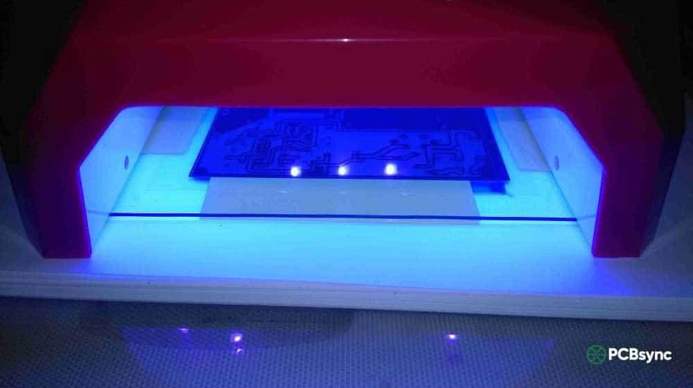
Step 4: UV Exposure
Exposure is where your circuit pattern transfers to the dry film. The exposed areas polymerize and become resistant to the developer solution.
Exposure Parameters
Light Source
Typical Exposure Time
Distance
Notes
350-400nm UV LED array
1-3 minutes
15-30cm
Most consistent results
15W fluorescent UV
3-5 minutes
5-10cm
Common hobby choice
Sunlight (midday)
10-15 minutes
N/A
Variable, harder to control
UV nail lamp
2-4 minutes
Direct contact
Works in a pinch
Exposure Process
Keep the Mylar on: The top protective film blocks oxygen that would inhibit polymerization. Don’t remove it until development.
Ensure contact: Your artwork must be in firm contact with the dry film. Use glass plates, a vacuum frame, or bulldog clips to hold everything tight.
Expose correctly: Under-exposure gives soft, poorly defined traces that wash away during development. Over-exposure causes resist brittleness and makes stripping difficult.
Wait after exposure: Let the board rest for at least 15 minutes before developing. This allows the polymerization reaction to complete.
Determining Optimal Exposure
The best way to find your sweet spot is to run a test strip:
Cut a small piece of laminated board
Cover it with your artwork
Use cardboard strips to cover sections progressively (uncover new section every 30 seconds)
Develop and examine which exposure gave the cleanest results
Step 5: Development
Development removes the unexposed (soft) PCB dry film, revealing the copper you want to etch. This is where your circuit pattern becomes visible.
Developer Solution Recipe
Chemical
Concentration
Temperature
Notes
Sodium carbonate (Na₂CO₃)
1% by weight (10g/L)
30-35°C (86-95°F)
Cheap and effective
Potassium carbonate (K₂CO₃)
0.85% by weight
30-35°C
Alternative to sodium
Mix 10 grams of sodium carbonate (washing soda) per liter of warm water. Fresh solution works best—don’t reuse developer that’s turned dark or has visible residue.
Development Process
Remove the Mylar layer: Peel off the top protective film just before developing
Immerse the board: Place it in the developer solution, pattern side up
Gentle agitation: Rock the tray or use a soft brush with minimal pressure. Never scrub—you’ll damage the resist
Watch for clearing: Unexposed film appears milky, then dissolves away. Development typically takes 2-5 minutes
Don’t over-develop: Once the copper is visible and the film is fully cleared, stop immediately
Rinse thoroughly: Use distilled water to stop the development process and remove any residue
Dry carefully: Use compressed air or let air dry. Don’t use heat at this point
Pro Tip: If your traces look fuzzy or partially developed, the issue is usually under-exposure—not development time. Check your UV source first.
Step 6: Etching
With your PCB dry film pattern developed, you’re ready to etch away the exposed copper. The resist protects your traces while the etchant removes everything else.
1. How long can I store laminated boards before exposure?
Laminated boards can be stored in complete darkness for up to 2 weeks without significant degradation. I’ve successfully used boards after one month of dark storage, but fresher is always better. If storing, wrap in black plastic and keep at room temperature.
2. Can I use sunlight instead of a UV exposure unit?
Yes, though it’s harder to control. Midday sunlight in summer provides strong UV—typically 10-15 minutes of exposure works. Winter sunlight is weaker and takes longer. The main challenge is consistency; clouds and time of day dramatically affect exposure. For reliable results, invest in a UV LED array or fluorescent UV box.
3. What’s the minimum trace width achievable with PCB dry film?
With proper technique and thin (0.8 mil) film, you can reliably achieve 50µm (2 mil) traces and spaces. Professional fab houses using 0.5 mil film can go down to 25µm. For home hobbyists, 100-150µm (4-6 mil) is a realistic target. Your limiting factor is usually artwork quality, not the dry film itself.
4. Why is my developed resist sticky or tacky?
Post-development stickiness indicates incomplete polymerization—usually under-exposure. Increase your exposure time by 25-50%. A quick fix is to dip the developed board briefly in dilute acid (like white vinegar), which neutralizes alkaline residue and hardens the surface. You can also post-expose the developed board to UV for 2-3 minutes.
5. Can I reuse developer solution?
Developer loses effectiveness as it absorbs dissolved photopolymer and as the carbonate reacts with carbon dioxide from air. Fresh solution gives the most consistent results. In practice, I’ll reuse developer for 2-3 boards before mixing a fresh batch. If development times start extending or you see residue on cleared areas, it’s time for new solution. At ~$0.50 per liter, fresh developer is cheap quality insurance.
Safety Considerations When Working with PCB Dry Film
Working with PCB dry film involves several chemicals that require proper handling. Don’t skip this section—I’ve learned some of these lessons the hard way.
Chemical Hazards
Sodium Hydroxide (Stripping Solution) This is the most dangerous chemical in the process. Even a 3% solution can cause serious burns. Always wear:
Chemical-resistant gloves (nitrile or rubber)
Safety glasses or goggles
Long sleeves
If you get NaOH on your skin, rinse immediately with plenty of water for at least 15 minutes. Keep a bottle of white vinegar nearby—it can help neutralize the base in an emergency.
Ferric Chloride (Etchant) Ferric chloride isn’t as caustic as NaOH, but it permanently stains everything it touches and is corrosive to metals. Work in a well-ventilated area and keep it away from sinks with metal drains. Dispose of spent etchant at your local hazardous waste facility—never pour it down the drain.
UV Exposure Don’t look directly at UV light sources. Even brief exposure can damage your eyes. If using a DIY UV box, ensure it’s fully enclosed when operating.
Environmental Disposal
Developer solution: Neutralize with acid (vinegar works), then dispose as normal waste
Stripper solution: Neutralize with acid before disposal
Ferric chloride: Take to hazardous waste collection—never drain
Dry film waste: Regular trash is fine; it’s not hazardous once cured
Advanced Tips for Professional Results
Once you’ve mastered the basics, here are some techniques that separate good boards from great ones:
Double-Sided Board Registration
For double-sided boards, alignment is everything. My method:
Drill small registration holes (1mm) in the corners before laminating
Use these holes to align your artwork on both sides
Laminate and expose one side completely
Flip, laminate the second side using pins through the registration holes
Consider collimated UV light to prevent undercutting
Reduce development time—fine lines dissolve faster
Use fresh, properly concentrated developer
Post-Development Hardening
For improved etch resistance, especially on complex boards:
After development, rinse thoroughly
Let the board dry completely
Give it a brief UV post-exposure (30 seconds to 1 minute)
This additional curing strengthens the resist
Conclusion: Master Your PCB Dry Film Process
PCB dry film photoresist has transformed home circuit board fabrication from an inconsistent art into a repeatable process. With the right materials, proper surface preparation, and attention to exposure and development parameters, you can produce boards that rival professional quality.
The learning curve is steeper than toner transfer, but the results are worth it. Fine-pitch components that were impossible with other methods become routine. Yields go up, frustration goes down, and you spend less time fixing bad boards.
Start with 1.0 mil film, nail down your lamination and exposure parameters with test strips, and document everything that works. Before long, you’ll wonder why you ever bothered with toner transfer.
Got questions about your specific setup? Drop them in the comments—I’ve probably troubleshot the same issue at some point.
Inquire: Call 0086-755-23203480, or reach out via the form below/your sales contact to discuss our design, manufacturing, and assembly capabilities.
Quote: Email your PCB files to Sales@pcbsync.com (Preferred for large files) or submit online. We will contact you promptly. Please ensure your email is correct.
Notes: For PCB fabrication, we require PCB design file in Gerber RS-274X format (most preferred), *.PCB/DDB (Protel, inform your program version) format or *.BRD (Eagle) format. For PCB assembly, we require PCB design file in above mentioned format, drilling file and BOM. Click to download BOM template To avoid file missing, please include all files into one folder and compress it into .zip or .rar format.


