Inquire: Call 0086-755-23203480, or reach out via the form below/your sales contact to discuss our design, manufacturing, and assembly capabilities.
Quote: Email your PCB files to Sales@pcbsync.com (Preferred for large files) or submit online. We will contact you promptly. Please ensure your email is correct.
Notes: For PCB fabrication, we require PCB design file in Gerber RS-274X format (most preferred), *.PCB/DDB (Protel, inform your program version) format or *.BRD (Eagle) format. For PCB assembly, we require PCB design file in above mentioned format, drilling file and BOM. Click to download BOM template To avoid file missing, please include all files into one folder and compress it into .zip or .rar format.
After 15 years of working in electronics manufacturing, I’ve seen countless engineers struggle with the PCB assembly process—not because it’s impossibly complex, but because finding clear, practical information in one place can be a challenge. This guide breaks down every stage of the PCB assembly process, from design verification to final testing, giving you the knowledge to work more effectively with your assembly partner or optimize your in-house operations.
Whether you’re launching your first prototype or scaling to high-volume production, understanding the PCB assembly process helps you make better design decisions, catch potential issues early, and ultimately build more reliable products.
What is the PCB Assembly Process?
The PCB assembly process (often abbreviated as PCBA) transforms a bare printed circuit board into a functional electronic assembly by mounting and soldering components onto it. Think of it this way: the bare PCB is like an empty city—the roads and infrastructure exist, but nothing actually happens until you add buildings, utilities, and people. Similarly, a PCB only becomes useful when populated with resistors, capacitors, integrated circuits, and all the other components that make your circuit work.
The process encompasses two main technologies:
Surface Mount Technology (SMT): Components are placed directly onto the board’s surface and soldered in a reflow oven
Through-Hole Technology (THT): Component leads pass through holes drilled in the board and are soldered on the opposite side
Most modern assemblies use a combination of both—SMT for the majority of components and through-hole for items that need extra mechanical strength, like large connectors and power components.
Before any components touch your board, the assembly process actually begins with design verification. This step alone can save you thousands of dollars and weeks of delays.
Design for Manufacturability (DFM) Check
A DFM check examines your PCB layout against the manufacturer’s fabrication capabilities. The goal is catching potential manufacturing problems while they’re still cheap to fix—during design, not production.
Key DFM verification points include:
Trace width and spacing: Minimum dimensions your fab house can reliably produce
Drill sizes and aspect ratios: Ensuring holes can be properly plated
Annular ring requirements: Adequate copper around drilled holes
Solder mask clearances: Proper dam widths between pads
Copper balance: Preventing warpage during thermal stress
Design for Assembly (DFA) Check
DFA focuses on whether your board can be efficiently assembled. This includes verifying:
Component footprint accuracy: Matching pads to actual component dimensions
Component spacing: Adequate clearance for pick-and-place equipment
Orientation markings: Clear polarity indicators for diodes, ICs, and electrolytic capacitors
Fiducial markers: Reference points for automated placement equipment
Panel optimization: Efficient use of production panels
Component placement, pad design, pick-and-place compatibility
Bill of Materials (BOM) Verification
Your BOM is the shopping list for assembly. Verification ensures:
Part numbers match actual components
Quantities are accurate
Footprints correspond to specified packages
Alternatives are identified for components with supply constraints
I’ve seen production runs delayed by weeks because someone specified a 0603 capacitor but the footprint was for an 0402. Catching this in DFM/DFA takes minutes; catching it during assembly costs days and money.
Step 1: Solder Paste Application
The PCB assembly process for SMT components begins with solder paste application. This gray, putty-like substance is a carefully formulated mixture of tiny solder spheres (typically 25-45 microns in diameter) suspended in flux.
The Stencil Printing Process
A precision-cut stainless steel stencil is aligned over the bare PCB. The stencil contains apertures (openings) that correspond exactly to the pads where components will be placed.
The process works like this:
The PCB is secured in a printing fixture
The stencil is aligned using fiducial markers
Solder paste is deposited on the stencil
A squeegee blade sweeps across, forcing paste through the apertures
The stencil lifts away, leaving precisely deposited paste on each pad
Solder Paste Composition
Modern lead-free solder paste typically uses SAC305 alloy:
Element
Percentage
Purpose
Tin (Sn)
96.5%
Primary bonding material
Silver (Ag)
3.0%
Improves wetting and joint strength
Copper (Cu)
0.5%
Reduces copper dissolution from pads
The flux component activates during heating to remove oxides and ensure proper wetting between the solder and the component leads.
Solder Paste Inspection (SPI)
Quality-focused assembly houses perform SPI immediately after printing. Using laser or camera-based systems, SPI measures:
Paste volume on each pad
Paste height consistency
Registration accuracy (paste alignment to pads)
Detection of bridging or insufficient deposits
Catching paste defects at this stage prevents downstream soldering failures and is far more cost-effective than finding issues after reflow.
Step 2: SMT Component Placement
With solder paste precisely applied, the board moves to pick-and-place machines—the workhorses of modern electronics assembly.
How Pick-and-Place Works
These machines are genuinely impressive pieces of engineering. A modern pick-and-place system:
Picks components from feeders (reels, trays, or tubes) using vacuum nozzles
Centers each component using optical alignment
Rotates the component to the correct orientation
Places it on the designated pad location with micron-level accuracy
Moves to the next component at speeds exceeding 100,000 placements per hour
The placement program is generated from your design files—specifically the centroid file (also called XY data or pick-and-place file) that specifies each component’s location, rotation, and reference designator.
Component Feeding Methods
Feed Type
Best For
Typical Components
Tape and Reel
High-volume, small components
Resistors, capacitors, small ICs
Tray
Larger or moisture-sensitive parts
BGAs, QFPs, connectors
Tube
Medium quantities, IC packages
DIP packages, some connectors
Loose/Bowl
Special handling requirements
Odd-form components
Placement Accuracy
Modern equipment achieves placement accuracy of ±25-50 microns—essential when working with fine-pitch components like 0.4mm pitch BGAs or 0201 passives. The tacky solder paste temporarily holds components in position until reflow soldering creates permanent connections.
Step 3: Reflow Soldering
Reflow soldering is where SMT assembly transforms from a collection of loosely held components into a permanently bonded assembly. Getting this step right is crucial—a poor reflow profile can damage components, create unreliable joints, or leave you with a board full of defects.
Understanding the Reflow Oven
Modern reflow ovens use convection heating with multiple independently controlled zones. As boards travel through on a conveyor, they experience a precisely choreographed temperature journey. High-end production ovens have 8-12 temperature zones, allowing fine control over the profile.
The oven’s atmosphere also matters. Nitrogen purging displaces oxygen, reducing oxidation of solder and component leads. While adding cost, nitrogen atmosphere improves wetting and reduces defects like head-in-pillow on BGA components.
The Reflow Profile
The board passes through a convection oven following a carefully controlled temperature profile with four distinct zones:
Preheat Zone (25°C to 150°C)
Ramp rate: 1-3°C per second
Purpose: Gradually raise board temperature, avoiding thermal shock to components
Duration: 60-90 seconds
Thermal Soak Zone (150°C to 200°C)
Purpose: Activate flux, remove volatiles, equalize temperature across the board
Duration: 60-120 seconds
Critical for reducing the temperature differential (Delta T) between small and large components
Reflow Zone (Peak: 235-250°C for lead-free)
Time above liquidus (TAL): 30-60 seconds
Purpose: Solder melts and wets component leads and pads
Peak temperature typically 20-40°C above solder liquidus point
Cooling Zone
Ramp rate: 2-4°C per second
Purpose: Solidify solder joints with proper grain structure
Controlled cooling prevents thermal shock and ensures joint reliability
Reflow Zone
Temperature Range
Duration
Purpose
Preheat
25°C → 150°C
60-90 sec
Gradual heating
Soak
150°C → 200°C
60-120 sec
Flux activation, thermal equalization
Reflow
Peak 235-250°C
30-60 sec TAL
Solder melting and wetting
Cooling
250°C → 25°C
Controlled descent
Joint solidification
Nitrogen Atmosphere
Many production lines use nitrogen during reflow to minimize oxidation. While this adds cost, it improves solder wetting and reduces defects like head-in-pillow on BGA packages.
Step 4: Automated Optical Inspection (AOI)
After reflow, the assembly undergoes its first major quality gate: Automated Optical Inspection.
What AOI Detects
Using high-resolution cameras and sophisticated image processing, AOI systems inspect for:
Missing components: Empty pads where components should be
Component presence: Verifying correct part at each location
Orientation errors: Reversed polarity or rotated parts
Wrong component values: Detecting incorrect parts (within visible marking limitations)
AOI Capabilities and Limitations
AOI excels at surface-level defects but cannot see hidden connections. This is particularly important for:
BGA solder balls (hidden under the package)
QFN ground pads (also hidden)
Internal PCB defects
For these, X-ray inspection is required.
Step 5: Through-Hole Component Assembly
Many boards combine SMT with through-hole components. After SMT assembly and inspection, through-hole parts are inserted—either manually or by automated insertion equipment.
Through-Hole Insertion Methods
Manual Insertion Used for low volumes, prototypes, or components that don’t suit automation. Operators insert components according to assembly drawings, typically using:
Component sequence guides
Anti-static workstations
Insertion tools for tight spaces
Automated Insertion High-volume production uses automated insertion equipment for components like:
Axial components (resistors, diodes)
Radial components (electrolytic capacitors)
DIP packages
Wave Soldering
For through-hole components, wave soldering is the traditional mass-soldering method:
Flux application: Spray or foam flux coats the bottom of the board
Preheating: Board temperature rises to 100-150°C to activate flux and reduce thermal shock
Wave contact: The board passes over a standing wave of molten solder (250-260°C for lead-free)
Cooling: Controlled cool-down solidifies joints
Wave soldering works well for pure through-hole boards but struggles with double-sided SMT assemblies where bottom-side components would be submerged in solder.
Selective Soldering
For mixed assemblies with SMT on both sides, selective soldering targets only the through-hole connections:
A programmable solder nozzle applies solder to specific locations
Bottom-side SMT components remain protected
Individual parameter control for each joint
Soldering Method
Best For
Throughput
Precision
Wave Soldering
High-volume THT, single-sided boards
Highest
Moderate
Selective Soldering
Mixed technology, double-sided boards
Moderate
High
Manual Soldering
Low volume, rework, specialized joints
Lowest
Operator-dependent
Step 6: X-Ray Inspection (AXI)
When you cannot see a solder joint, you need to look through it. X-ray inspection (Automated X-ray Inspection, or AXI) is essential for:
Flying probe testers use movable probes instead of a fixed fixture, trading speed for flexibility—ideal for prototype runs where custom fixtures aren’t economical.
Step 8: Functional Testing
While ICT verifies components, functional testing confirms the assembled board actually works as designed.
Functional Test Scope
Depending on the product, functional testing may include:
Power-on testing: Verifying power supply rails, current consumption
Signal integrity: Checking waveforms, timing, signal levels
Communication verification: Testing serial buses (I2C, SPI, UART), wireless links
ICT verifies electrical connectivity and component values
Functional test confirms the design works as intended
Each layer catches different defect types; together they provide comprehensive quality assurance.
Step 9: Cleaning and Conformal Coating
Depending on your product’s requirements, post-assembly processing may include cleaning and protective coating.
PCB Cleaning
Flux residues left after soldering can cause long-term reliability issues if not addressed:
No-clean flux: Designed to leave benign residues—often acceptable without cleaning
Water-soluble flux: Requires deionized water washing
Rosin flux: May require solvent or aqueous cleaning
Cleaning methods:
Batch spray washers
Inline conveyorized washers
Ultrasonic cleaning for tight spaces
Conformal Coating
For products exposed to harsh environments, conformal coating provides a protective barrier:
Coating Type
Protection Level
Typical Applications
Acrylic
Moderate
Consumer electronics
Silicone
Good thermal range
Automotive, LED
Polyurethane
Excellent chemical resistance
Industrial, military
Epoxy
Maximum protection
Aerospace, harsh environments
Application methods include selective spray, dip coating, and brush application.
Step 10: Final Quality Control and Packaging
The final station in the PCB assembly process involves comprehensive quality verification and preparation for shipping.
Final QC Inspection
Visual inspection for workmanship issues
Verification of correct part markings and labels
Dimensional checks if required
Documentation verification (test records, certificates of conformance)
ESD-Safe Packaging
Electronic assemblies are sensitive to electrostatic discharge throughout their lifecycle:
Anti-static bags (pink poly or metalized shielding bags)
Moisture barrier bags with desiccant for moisture-sensitive assemblies
Proper labeling including date codes and lot traceability
Appropriate cushioning for shipping
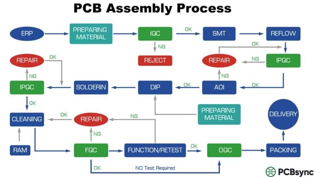
PCB Assembly Process Flow Chart Summary
Here’s the complete PCB assembly process at a glance:
Step
Process
Key Purpose
0
DFM/DFA Check
Prevent manufacturing issues
1
Solder Paste Application
Deposit solder on SMT pads
2
SMT Placement
Position surface-mount components
3
Reflow Soldering
Permanently bond SMT components
4
AOI Inspection
Detect surface-level defects
5
Through-Hole Assembly
Insert and solder THT components
6
X-Ray Inspection
Inspect hidden connections
7
In-Circuit Testing
Verify electrical connectivity
8
Functional Testing
Confirm operational performance
9
Cleaning/Coating
Remove residues, apply protection
10
Final QC & Packaging
Quality verification, shipping prep
SMT vs Through-Hole: Choosing the Right Assembly Technology
One question I get asked frequently is when to use SMT versus through-hole components. The answer isn’t always straightforward, and understanding the tradeoffs helps you make better design decisions.
When to Choose SMT
Surface mount technology dominates modern electronics for good reasons:
Size and density: SMT components are dramatically smaller. A 0402 resistor measures just 1.0mm x 0.5mm—you could fit dozens where a single through-hole resistor would go. This enables the compact devices we use every day.
Speed: Pick-and-place machines can place SMT components at rates exceeding 100,000 components per hour. The automated reflow process then solders them all simultaneously. Through-hole assembly is inherently slower.
Cost: At volume, SMT assembly costs less per component due to automation efficiency and smaller board sizes.
Double-sided assembly: SMT components can be placed on both sides of the board, effectively doubling available real estate.
When Through-Hole Still Makes Sense
Despite SMT’s advantages, through-hole technology remains essential for specific applications:
High mechanical stress: Connectors that get plugged and unplugged repeatedly benefit from the mechanical anchor that through-hole leads provide. The solder joint extends through the board, creating a much stronger physical connection.
High power components: Power resistors, large capacitors, and transformers often use through-hole mounting for better thermal dissipation and mechanical stability.
Manual assembly considerations: If your product will be hand-assembled or repaired in the field, through-hole components are easier to work with using basic soldering equipment.
Legacy compatibility: Some specialized components simply aren’t available in surface-mount packages.
The Reality: Mixed Technology
Most production boards use both technologies. A typical design might have:
90%+ SMT components (resistors, capacitors, ICs)
Through-hole for connectors, mounting hardware, and high-power components
This mixed approach lets you optimize each component choice while keeping the overall assembly process efficient.
Tips for a Successful PCB Assembly Process
Based on years of working with assembly houses and troubleshooting production issues, here are practical tips that can save you headaches:
Design Phase Tips
Work with your assembler early: Don’t wait until your design is complete to engage your assembly partner. Their DFM feedback during design saves redesign cycles.
Use standard footprints: Custom footprints are a common source of assembly problems. Use manufacturer-recommended land patterns or IPC-7351 standards.
Consolidate component values: Every unique part number adds procurement and inventory complexity. Standardizing on common values (10K resistors, 100nF capacitors) reduces BOM cost and supply chain risk.
Include test points: Design for testability from the start. Adding test access after layout is much harder than including it initially.
Mind your thermal relief: Components on large copper pours need thermal relief patterns, or they’ll act as heat sinks during soldering, causing cold joints.
Documentation Tips
Complete BOM information: Include manufacturer part numbers, not just values and packages. “10K 0603 resistor” leaves room for interpretation; a specific MPN doesn’t.
Clear assembly drawings: Mark component reference designators clearly. Indicate polarity for every polarized component. Include any special instructions.
Version control everything: Use revision numbers and dates on all documentation. Nothing causes more assembly confusion than mismatched file versions.
Communication Tips
Ask questions proactively: If something seems unclear, ask. Assembly technicians can’t read your mind, and assumptions lead to expensive mistakes.
Review the first article: Before production runs, request and carefully inspect a first article sample. This catches issues before they’re multiplied across hundreds of boards.
Establish change control: Any design change—even minor ones—should be formally communicated to your assembler with updated documentation.
Understanding PCB Assembly Costs
Cost is always a consideration, and understanding what drives assembly pricing helps you optimize your design and purchasing decisions.
Cost Factors in PCB Assembly
Component count: More components = more placement operations = higher cost. But don’t sacrifice functionality to reduce count—optimize by consolidating where possible.
Component types: Standard SMT parts are cheapest to place. BGAs, fine-pitch QFPs, and 0201/01005 packages require more precision and cost more. Through-hole components add manual handling or wave soldering steps.
Board complexity: Double-sided assembly costs more than single-sided. High layer counts, tight tolerances, and special finishes add cost.
Quantity: Setup costs (programming, stencils, fixtures) get amortized over volume. A 10-piece prototype run has much higher per-unit cost than a 10,000-piece production run.
Turnaround time: Quick-turn services command premium pricing. Standard lead times are more economical.
Turnkey vs Consigned Assembly
Turnkey assembly: The assembly house procures all components and bare boards. You provide documentation; they handle everything else. More convenient but typically higher cost.
Consigned assembly: You provide all components and bare boards; they perform assembly only. Lower cost but requires you to manage procurement and inventory.
Partial turnkey: You provide specialty or long-lead components; they source common parts. A middle ground that can optimize both cost and convenience.
Assembly Model
Your Responsibility
Cost
Best For
Full Turnkey
Documentation only
Highest
Convenience, low volume
Partial Turnkey
Long-lead/specialty parts
Medium
Cost optimization
Consigned
All components, boards
Lowest
High volume, controlled supply chain
Common PCB Assembly Defects and Solutions
Understanding common defects helps you design boards that avoid them:
Defect
Cause
Prevention
Solder bridging
Excessive paste, tight pitch
Proper stencil design, adequate pad spacing
Tombstoning
Uneven heating, pad imbalance
Thermal balance in layout, component orientation
Cold solder joint
Insufficient heat, contamination
Proper reflow profile, clean boards
Voiding
Trapped flux gases, moisture
Profile optimization, proper storage
Head-in-pillow
BGA warpage, oxidation
Nitrogen reflow, pre-bake components
Missing components
Placement error, lost parts
Proper programming, vacuum verification
IPC Standards for PCB Assembly
The electronics industry relies on IPC standards for consistent quality. Key standards you s
hould know:
Standard
Scope
IPC-A-610
Acceptability of Electronic Assemblies
IPC J-STD-001
Requirements for Soldered Electrical and Electronic Assemblies
IPC-7711/7721
Rework, Modification, and Repair of Electronic Assemblies
IPC-A-600
Acceptability of Printed Boards
IPC-2221
Generic Standard on Printed Board Design
IPC Classes Explained
IPC defines three product classes based on reliability requirements:
Class 1: General Electronics—consumer products where cosmetic imperfections are acceptable if function is maintained
Class 2: Dedicated Service Electronics—communication equipment, industrial controls where extended life is expected
Class 3: High Reliability Electronics—aerospace, medical, military where failure is unacceptable
PCB Assembly for Different Industries
The PCB assembly process adapts to different industry requirements. Understanding these variations helps you select the right assembly partner and specify appropriate requirements.
IPC Designer Council: Training and certification resources
Frequently Asked Questions
What is the difference between PCB and PCBA?
A PCB (printed circuit board) is the bare board—the substrate with copper traces, vias, and pads but no components. Think of it as the foundation and roadways of a city. PCBA (printed circuit board assembly) is the same board after components have been mounted and soldered, making it a functional electronic assembly—the city with all its buildings, utilities, and inhabitants.
The PCB is a component that you purchase from a fabrication house. The PCBA is a finished or semi-finished product that results from the assembly process, ready for integration into your end product.
How long does PCB assembly typically take?
Timeline varies significantly based on complexity, quantity, and assembly house capacity:
Prototype (quick-turn): 24 hours to 5 days for small quantities
Turnkey services (where the assembly house procures components) typically add 1-2 weeks for component sourcing, depending on availability. Component lead times have become increasingly variable, so always confirm availability before committing to schedules.
The fastest turnaround requires having components in stock, design files ready, and working with an assembly partner who offers expedited services.
What files are needed for PCB assembly?
Minimum requirements:
Gerber files: PCB Manufacturing data for the bare board (copper layers, solder mask, silkscreen, drill files)
BOM (Bill of Materials): Component list with part numbers, values, package types, and reference designators
Centroid/XY file: Component placement coordinates and rotation angles
Assembly drawing: Visual reference showing component placement, orientation, and any special notes
Additional helpful files:
Schematic (PDF or native format) for reference
Test documentation and test point locations
Special assembly instructions for sensitive components
CAD files in native format (Altium, KiCad, Eagle)
Many assembly houses accept ODB++ or IPC-2581 formats, which bundle all necessary data into a single intelligent package.
What is the difference between SMT and THT assembly?
SMT (Surface Mount Technology) places components directly on the board surface using solder paste deposited through a stencil. Components are held in place by paste tackiness until reflow soldering permanently bonds them. SMT allows smaller components, higher density, and automated assembly at very high speeds. Most modern electronics use predominantly SMT assembly.
THT (Through-Hole Technology) inserts component leads through holes drilled in the board. These leads are then soldered on the opposite side using wave soldering, selective soldering, or manual techniques. THT provides stronger mechanical connections, making it preferred for connectors, high-power components, and parts subject to mechanical stress.
Most modern assemblies use both technologies—SMT for the majority of components and THT for specific applications requiring mechanical robustness.
How do I choose between different assembly houses?
Key evaluation criteria:
Technical capabilities: Do they handle your board complexity? Consider layer count, component types (BGAs, fine-pitch, 0201s), tolerances, and special requirements.
Certifications: ISO 9001 is baseline. Industry-specific certifications matter: AS9100 for aerospace, ISO 13485 for medical, IATF 16949 for automotive.
Volume fit: Some houses specialize in prototypes and quick-turn, others in high-volume production. Mixing these often results in poor service or pricing.
Location: Domestic assembly offers easier communication and faster turnaround. Offshore assembly (often China) typically costs less but requires longer lead times and careful quality management.
DFM support: Quality partners provide meaningful DFM feedback that improves your design. This support is invaluable, especially for complex boards.
Test capabilities: Confirm they have AOI, X-ray (if you have BGAs), ICT, and functional test capabilities appropriate to your product.
References and track record: Ask for references from customers with similar products. A house that excels at consumer electronics may struggle with medical devices, and vice versa.
Inquire: Call 0086-755-23203480, or reach out via the form below/your sales contact to discuss our design, manufacturing, and assembly capabilities.
Quote: Email your PCB files to Sales@pcbsync.com (Preferred for large files) or submit online. We will contact you promptly. Please ensure your email is correct.
Notes: For PCB fabrication, we require PCB design file in Gerber RS-274X format (most preferred), *.PCB/DDB (Protel, inform your program version) format or *.BRD (Eagle) format. For PCB assembly, we require PCB design file in above mentioned format, drilling file and BOM. Click to download BOM template To avoid file missing, please include all files into one folder and compress it into .zip or .rar format.


