Inquire: Call 0086-755-23203480, or reach out via the form below/your sales contact to discuss our design, manufacturing, and assembly capabilities.
Quote: Email your PCB files to Sales@pcbsync.com (Preferred for large files) or submit online. We will contact you promptly. Please ensure your email is correct.
Notes: For PCB fabrication, we require PCB design file in Gerber RS-274X format (most preferred), *.PCB/DDB (Protel, inform your program version) format or *.BRD (Eagle) format. For PCB assembly, we require PCB design file in above mentioned format, drilling file and BOM. Click to download BOM template To avoid file missing, please include all files into one folder and compress it into .zip or .rar format.
10 PCB Assembly Problems Solved by Proper DFA Design
Every engineer who’s waited anxiously for first articles from assembly knows this feeling: the email arrives, you open the inspection report, and there it is—tombstoned capacitors, solder bridges, misaligned BGAs. Another round of rework, another delayed shipment, another difficult conversation with the customer. These PCB assembly problems aren’t random acts of manufacturing chaos. They’re predictable failures that proper Design for Assembly (DFA) practices could have prevented.
After two decades of designing boards and troubleshooting assembly failures, I’ve learned that most production issues trace back to design decisions made weeks before the first component was placed. DFA isn’t about making your manufacturer’s life easier (though it does). It’s about designing boards that build right the first time, every time.
Design for Assembly is a systematic approach to optimizing your PCB layout for efficient, error-free component placement and soldering. While Design for Manufacturing (DFM) asks “can we fabricate this board?”, DFA asks “can we assemble it reliably?”
DFA encompasses three critical phases:
Layout Phase: Component placement, spacing, orientation, and thermal considerations during schematic-to-layout conversion
Validation Phase: Checking Gerber files, pick-and-place data, and BOM against footprints and manufacturer capabilities
Process Phase: Ensuring your design supports wave soldering, reflow soldering, or mixed assembly processes as required
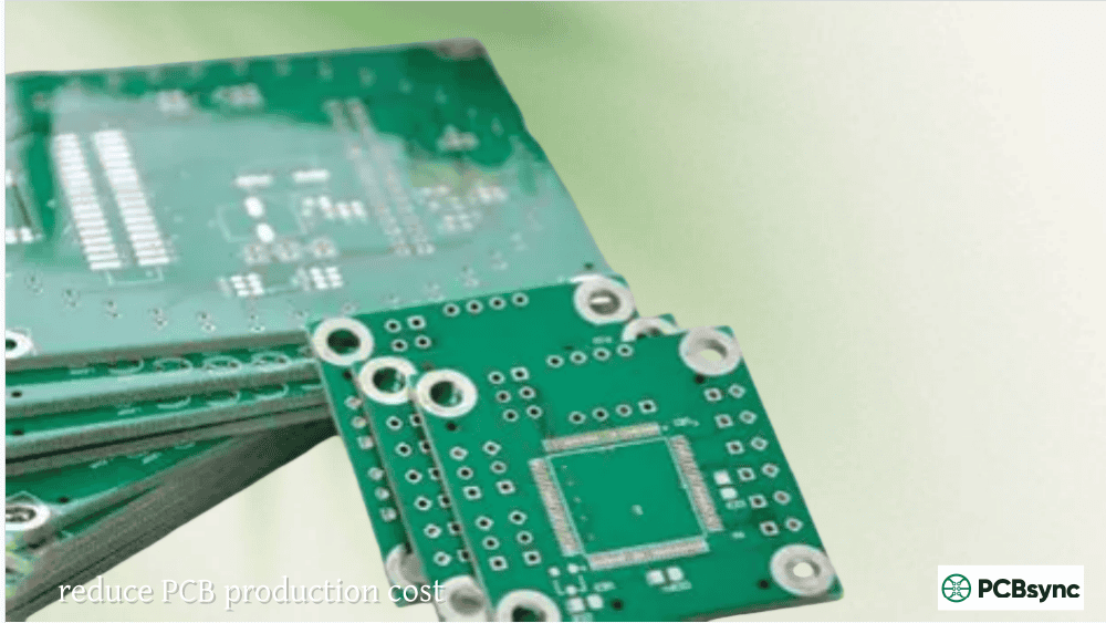
The investment in DFA pays dividends throughout production. Boards designed with assembly in mind achieve higher first-pass yields, require less rework, and transition smoothly from prototype to volume production.
10 Critical PCB Assembly Problems and Their DFA Solutions
Problem 1: Component Tombstoning
Tombstoning occurs when one end of a small passive component lifts off its pad during reflow, leaving the part standing vertically like a tombstone. It’s one of the most frustrating PCB assembly problems because it creates open circuits in components that look almost correctly placed.
Root Causes:
Unequal pad sizes creating thermal imbalance
Different trace widths connecting to each pad
One pad thermally coupled to ground plane
Uneven solder paste deposition
DFA Solution:
Design Element
Tombstoning Prevention
Pad geometry
Use identical pad sizes on both ends
Trace connections
Match trace widths entering each pad
Thermal relief
Apply to pads connected to copper pours
Component orientation
Orient consistently relative to reflow direction
Paste apertures
Ensure stencil provides equal paste volume
For 0402 and smaller components, thermal balance becomes critical. If one pad connects to a ground plane while the other connects only to a trace, add thermal relief to the plane connection so both pads heat at similar rates during reflow.
Problem 2: Solder Bridging Between Pads
Solder bridges create unintended electrical connections between adjacent pads, causing shorts that may pass initial visual inspection but fail functional testing. Fine-pitch components like QFPs and BGAs are particularly susceptible.
Root Causes:
Insufficient solder mask between pads
Excessive solder paste volume
Pads too close together for stencil design
Component misalignment during placement
DFA Solution: Maintain adequate solder mask dams between pads. Per IPC guidelines, design for minimum 4 mil solder mask width between pad edges. For fine-pitch components (0.5mm pitch and below), ensure your stencil design accounts for paste slump and reflow spreading.
Review pad-to-pad spacing against your assembly house’s capabilities. A common DFA rule is minimum 10 mils between SMT pad edges, with 20-30 mils preferred for reliable processing.
Problem 3: BOM and Footprint Mismatches
Nothing stops an assembly line faster than discovering the components don’t fit the footprints. This PCB assembly problem wastes time, money, and production capacity while engineers scramble to identify whether the BOM or layout is wrong.
Common Mismatch Scenarios:
BOM specifies 0402 resistor, layout has 0603 footprint
Component package changed during design but footprint wasn’t updated
Pin numbering differs between datasheet and library part
Metric vs. imperial package size confusion
DFA Solution:
Validation Step
What to Check
Part number verification
Cross-reference every MPN against manufacturer datasheet
Footprint validation
Compare pad dimensions to component drawing
Pin mapping
Verify pin 1 location matches component and symbol
Package confirmation
Check actual package dimensions, not just nominal size
Implement a formal BOM-to-layout validation process before releasing design files. Many EDA tools offer automated footprint verification against component databases—use these features rather than trusting that library parts are correct.
Problem 4: Insufficient Component Clearances
When components are placed too close together, pick-and-place machines can’t grip them properly, rework becomes impossible, and wave soldering creates shadowing effects. This is among the most common PCB assembly problems in space-constrained designs.
DFA Solution: Follow spacing guidelines based on component types and assembly processes:
Component Type
Minimum Spacing
Recommended Spacing
SMD to SMD
10 mils (0.25mm)
20-30 mils
SMD to THT
40 mils (1.0mm)
60 mils
Tall component to short
50 mils
100 mils
Any component to board edge
100 mils
125 mils
Component to test point
50 mils
100 mils
For wave soldering, orient components so taller parts don’t shadow shorter parts from the solder wave. Place smaller components first in the wave direction to prevent the “shadowing effect” that causes insufficient solder joints.
Problem 5: Poor Thermal Management During Soldering
Components with thermal pads or large ground connections can act as heat sinks during reflow, preventing proper solder joint formation. This PCB assembly problem manifests as cold joints, insufficient wetting, or components that shift during extended reflow exposure.
Root Causes:
Large copper areas connected directly to pads
Missing thermal reliefs on ground connections
Thermal pad design preventing proper heat transfer
Inadequate reflow time for heavy thermal loads
DFA Solution: Always use thermal reliefs on pads connected to copper pours or planes. For exposed thermal pads (common on power components and QFNs), work with your assembly house on stencil design. Segmented stencil apertures using “window pane” or cross-hatch patterns allow volatiles to escape and reduce voiding under thermal pads.
Include thermal analysis in your DFA review. Identify components with significant thermal mass and ensure the reflow profile can adequately heat them without damaging temperature-sensitive parts elsewhere on the board.
Problem 6: Incorrect Component Orientation and Polarity
Reversed polarity on diodes, capacitors, or ICs can destroy components on first power-up. Inconsistent component orientation slows manual assembly and increases pick-and-place programming complexity.
DFA Solution:
Polarity/Orientation Issue
Prevention Method
Diode polarity
Clear cathode marking on silkscreen, footprint
Electrolytic capacitor polarity
Mark positive terminal, verify against datasheet
IC pin 1 location
Consistent pin 1 indicator on silkscreen and copper
Connector orientation
Physical keying where possible, clear marking
LED polarity
Cathode indicator on silkscreen
Orient all similar components in the same direction when possible. This simplifies pick-and-place programming, speeds visual inspection, and reduces the chance of insertion errors during manual assembly or rework.
Problem 7: Missing or Incorrect Fiducials
Fiducials are the reference marks that automated pick-and-place machines use to locate component positions. Without proper fiducials, placement accuracy suffers, leading to misaligned components and assembly defects.
DFA Solution: Include both global and local fiducials in your design:
Global Fiducials: Place at least three fiducials asymmetrically near board corners for overall board registration. Use 1mm diameter copper circles with 2mm solder mask clearance.
Local Fiducials: Add fiducials near fine-pitch components (BGAs, QFPs with pitch ≤0.5mm) to improve local placement accuracy. Position them within 50mm of the component.
Ensure fiducials are:
On copper layer with solder mask opening
Not covered by silkscreen
At least 5mm from board edges
Consistent size throughout the design
Problem 8: Panelization and Depanelization Issues
Poor panel design causes components to crack during depanelization, boards to warp in reflow ovens, or individual boards to separate prematurely during assembly. These PCB assembly problems multiply across every board in the panel.
Root Causes:
Components too close to breakaway tabs
V-score lines passing through sensitive areas
Unbalanced panel causing warpage
Inadequate support during assembly
DFA Solution: Maintain minimum 100 mils clearance between components and board edges where depanelization occurs. For v-scored panels, this clearance prevents mechanical stress from cracking solder joints. For routed tabs, ensure breakaway points won’t leave burrs that affect enclosure fit.
Design panels with balanced copper distribution to minimize warpage during reflow. Consider adding tooling holes and breakaway rails that provide consistent support throughout the assembly process.
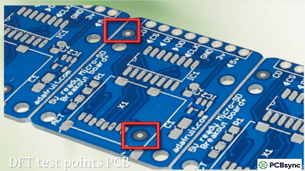
Problem 9: Inadequate Test Access
Boards that can’t be tested efficiently become quality bottlenecks. Missing test points, inaccessible nodes, and designs incompatible with bed-of-nails fixtures force reliance on expensive flying probe testing or incomplete functional testing.
DFA Solution: Design for testability (DFT) should be part of your DFA process:
Test Access Requirement
DFA Guideline
Test point size
Minimum 35 mil diameter, 50 mil preferred
Test point spacing
Minimum 100 mil center-to-center
Test point location
Accessible from one side of board
Critical node access
Every power rail, ground, key signals
Clearance from components
Minimum 50 mil from nearest part
If using bed-of-nails testing, ensure test points align to a standard grid (typically 100 mil) and don’t conflict with component placement. Include test points for all critical nets, not just power and ground.
Problem 10: Documentation and File Errors
Incomplete or inconsistent documentation creates confusion during assembly, leading to wrong component placements, incorrect orientations, and builds that don’t match design intent. This is a particularly insidious PCB assembly problem because it may not be caught until functional testing.
Common Documentation Errors:
Centroid file coordinates don’t match Gerber data
BOM revision doesn’t match layout revision
Missing assembly drawings for variant builds
Unclear DNI (Do Not Install) designations
Silkscreen conflicts with solder mask openings
DFA Solution: Create a complete documentation package that includes:
Gerber files with clear layer naming conventions
Drill files with accurate hole counts and sizes
Centroid/pick-and-place file with consistent units and rotation
BOM with full manufacturer part numbers and alternates
Assembly drawings showing top and bottom views
Special instructions for any non-standard processes
Before release, verify that all files reference the same design revision. Check that centroid coordinates align with actual component positions in the layout. Confirm layer polarity and units are consistent across all files.
DFA Implementation Best Practices
Start DFA During Schematic Capture
Component selection during schematic design affects assembly outcomes. Consider:
Package availability and standardization
Lead pitch and assembly complexity
Thermal requirements and pad design
End-of-life status and second sources
Communicate with Your Assembly Partner
Different assembly houses have different capabilities. Before finalizing your layout:
Request their specific DFA guidelines
Understand their equipment limitations
Discuss any non-standard requirements
Review thermal profiles for your component mix
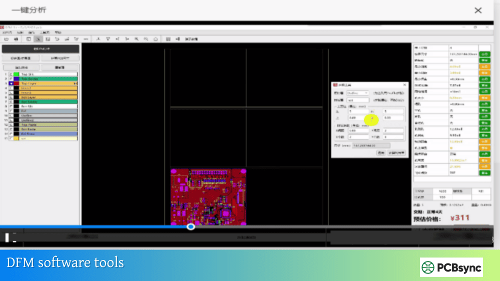
Use Automated DFA Checking
Modern EDA tools include DFA rule checking capabilities. Configure these tools with your assembly house’s specific requirements to catch issues before Gerber release.
Resources for DFA Implementation
Industry Standards
IPC-7351: Generic requirements for surface mount land patterns
IPC-A-610: Acceptability of electronic assemblies
IPC-2221: Generic standard on printed board design
IPC-2581: Generic requirements for PCB assembly data transfer
DFA Analysis Tools
Valor NPI (Siemens): Comprehensive DFM/DFA analysis
Frequently Asked Questions About PCB Assembly Problems
What is the difference between DFM and DFA?
DFM (Design for Manufacturing) focuses on bare board fabrication—ensuring traces, vias, and copper features can be manufactured successfully. DFA (Design for Assembly) focuses on component placement and soldering—ensuring parts can be reliably placed and soldered to the fabricated board. Both are essential; a board that fabricates perfectly but can’t be assembled efficiently still fails in production. Together, they form DFMA (Design for Manufacturing and Assembly), a comprehensive approach to production-ready design.
When should DFA analysis begin in the design process?
DFA considerations should start during schematic capture when selecting components and packages. Early decisions about component sizes, package types, and pin configurations directly impact assembly outcomes. Formal DFA analysis should run after initial component placement and again before Gerber release. The earlier you identify potential PCB assembly problems, the less expensive they are to fix.
Can DFA software catch all assembly problems?
Automated DFA tools catch many common issues but can’t identify every potential problem. They excel at checking spacing rules, footprint validation, and documentation completeness. However, they may miss issues related to thermal interactions between specific components, assembly sequence dependencies, or problems unique to your assembly partner’s equipment. Automated analysis should complement, not replace, review by experienced engineers and your assembly partner.
How much does poor DFA cost in production?
Studies suggest that PCB assembly problems caught during production cost 10-100 times more to fix than issues caught during design review. A single tombstoning issue might require hand rework on every affected board, adding labor costs and creating quality variability. More severe issues like BOM-footprint mismatches can halt production entirely while replacement parts are sourced or boards are redesigned. The cost of thorough DFA analysis is trivial compared to production firefighting.
Should I use my assembly house’s DFA service or do my own analysis?
Both approaches add value and should be used together. Running your own DFA analysis during design catches issues early when changes are easy. Your assembly house’s DFA review validates your design against their specific equipment and processes—capabilities that may differ from generic DFA rules. Think of internal DFA as development testing and assembly house DFA as acceptance testing. Skipping either increases your risk of PCB assembly problems reaching production.
Building Assembly Success Into Every Design
PCB assembly problems aren’t inevitable—they’re designable. Every issue covered in this article has a design-phase solution. Tombstoning can be eliminated with balanced pad design. Solder bridging disappears with adequate mask dams. BOM mismatches vanish with proper validation processes.
The engineers whose boards glide through assembly aren’t lucky. They’ve internalized DFA thinking so deeply that assembly-friendly decisions happen automatically during layout. They communicate with their assembly partners early and often. They use every tool available—automated checking, design reviews, and pcb manufacturing feedback—to catch issues before they become production problems.
The choice is yours: spend time on DFA during design, or spend far more time troubleshooting assembly failures after the fact. The boards you design today will either build smoothly or create headaches for everyone in the production chain. Proper DFA ensures they build right the first time.
Inquire: Call 0086-755-23203480, or reach out via the form below/your sales contact to discuss our design, manufacturing, and assembly capabilities.
Quote: Email your PCB files to Sales@pcbsync.com (Preferred for large files) or submit online. We will contact you promptly. Please ensure your email is correct.
Notes: For PCB fabrication, we require PCB design file in Gerber RS-274X format (most preferred), *.PCB/DDB (Protel, inform your program version) format or *.BRD (Eagle) format. For PCB assembly, we require PCB design file in above mentioned format, drilling file and BOM. Click to download BOM template To avoid file missing, please include all files into one folder and compress it into .zip or .rar format.


