Inquire: Call 0086-755-23203480, or reach out via the form below/your sales contact to discuss our design, manufacturing, and assembly capabilities.
Quote: Email your PCB files to Sales@pcbsync.com (Preferred for large files) or submit online. We will contact you promptly. Please ensure your email is correct.
Notes: For PCB fabrication, we require PCB design file in Gerber RS-274X format (most preferred), *.PCB/DDB (Protel, inform your program version) format or *.BRD (Eagle) format. For PCB assembly, we require PCB design file in above mentioned format, drilling file and BOM. Click to download BOM template To avoid file missing, please include all files into one folder and compress it into .zip or .rar format.
I’ve been designing wireless circuits for over a decade now, and I can tell you that the PCB antenna is often the most underestimated component in any RF design. Engineers spend weeks perfecting their microcontroller code or optimizing power consumption, only to slap on an antenna as an afterthought. The result? Poor range, failed EMC tests, and frustrated customers.
In this guide, I’m going to walk you through everything you need to know about PCB antenna design—from selecting the right type for your application to calculating dimensions and avoiding the rookie mistakes that cost me countless prototype revisions early in my career.
A PCB antenna (also called an embedded antenna, on-board antenna, or printed antenna) is an antenna whose radiating element is etched directly onto the printed circuit board using copper traces. Instead of requiring a separate antenna component or external whip, the antenna becomes part of the PCB itself.
This approach has become incredibly popular in modern electronics for several reasons:
Cost reduction: No separate antenna component means lower BOM costs
Space savings: The antenna integrates directly into the board layout
Design flexibility: Custom shapes can fit almost any enclosure
The trade-off? PCB antennas typically have lower efficiency and narrower bandwidth compared to dedicated external antennas. But for most IoT, Bluetooth, Wi-Fi, and short-range wireless applications, that trade-off is perfectly acceptable.
Antenna PCB Calculator
PCBSync Engineering Tools
Rectangular Patch Antenna Calculator
Calculated Dimensions
Patch Width (W)—
Patch Length (L)—
Effective εr—
Feed Point (from edge)—
Ground Plane (min)—
Visual Reference
W × L Patch
WLh
—
Wavelength (λ₀)
—
Est. Bandwidth
—
Est. Gain
W = c / (2f₀) × √(2/(εr+1))
L = c / (2f₀√εeff) – 2ΔL
ΔL = 0.412h × (εeff+0.3)(W/h+0.264) / (εeff-0.258)(W/h+0.8)
Design Tip
For optimal bandwidth, substrate height should be 0.003λ₀ to 0.05λ₀. Thicker substrates increase bandwidth but may excite surface waves. Rogers RO4003C offers excellent performance for most antenna applications with good thermal stability.
Microstrip Line Calculator
Microstrip Parameters
Trace Width—
Effective εr—
λ/4 Length—
λ/2 Length—
W/h Ratio—
Quarter-Wave Transformer
Transformer Parameters
Required Z₀—
λ/4 Length—
RF/Microwave Substrate Materials Database
Rogers RO4003C
Dielectric (εr)3.55 ±0.05
Loss Tangent0.0027
Tg>280°C
Best ForGeneral RF
Rogers RO4350B
Dielectric (εr)3.38 ±0.05
Loss Tangent0.0037
Tg>280°C
Best ForUHF-Microwave
Rogers RT/duroid 5880
Dielectric (εr)2.2 ±0.02
Loss Tangent0.0009
TgN/A (PTFE)
Best FormmWave
Rogers RO3003
Dielectric (εr)3.0 ±0.04
Loss Tangent0.0013
TgN/A
Best ForPhased Arrays
FR-4 Standard
Dielectric (εr)4.2-4.6
Loss Tangent0.02
Tg130-140°C
Best For<2 GHz
Rogers RO3006
Dielectric (εr)6.15 ±0.15
Loss Tangent0.0025
TgN/A
Best ForSize Reduction
High-Tg FR-4
Dielectric (εr)4.2 ±0.2
Loss Tangent0.015
Tg170°C
Best ForBudget RF
Rogers RO3010
Dielectric (εr)10.2 ±0.3
Loss Tangent0.0023
TgN/A
Best ForMiniaturization
Material Selection Guide
Choose Rogers RO4003C or RO4350B for general antenna applications up to 10 GHz. For mmWave (>24 GHz), use RT/duroid 5880 or similar PTFE materials. FR-4 is suitable only for sub-2 GHz applications where cost is critical.
Common Antenna Frequency Bands Reference
Band / Standard
Frequency Range
Wavelength
Type
Applications
GPS L1
1575.42 MHz
190.3 mm
GPS
Navigation, Timing
GPS L2
1227.60 MHz
244.3 mm
GPS
Precision Navigation
GPS L5
1176.45 MHz
254.8 mm
GPS
Safety-of-Life
WiFi 2.4 GHz
2.400 – 2.4835 GHz
124.9 mm
WiFi
802.11b/g/n/ax
WiFi 5 GHz
5.150 – 5.850 GHz
58.3 mm
WiFi
802.11a/n/ac/ax
WiFi 6E / 7
5.925 – 7.125 GHz
50.6 mm
WiFi
802.11ax/be
Bluetooth
2.402 – 2.480 GHz
124.8 mm
IoT
BLE, Classic BT
LoRa 868
863 – 870 MHz
347 mm
IoT
LPWAN Europe
LoRa 915
902 – 928 MHz
328 mm
IoT
LPWAN Americas
LTE Band 7
2500 – 2690 MHz
120 mm
Cellular
4G LTE
5G n78
3.3 – 3.8 GHz
90.9 mm
Cellular
5G Sub-6 GHz
5G mmWave n260
37 – 40 GHz
8.1 mm
Cellular
5G mmWave
Zigbee
2.400 – 2.4835 GHz
124.9 mm
IoT
Home Automation
Thread/Matter
2.400 – 2.4835 GHz
124.9 mm
IoT
Smart Home
UWB
6.0 – 8.5 GHz
50 mm
IoT
Ranging, Location
NFC
13.56 MHz
22.1 m
IoT
Contactless
Quick Wavelength Calculator
Wavelength Results
Free Space λ₀124.91 mm
λ/2 (Half-wave)62.45 mm
λ/4 (Quarter-wave)31.23 mm
Antenna PCB Stackup Designer
Stackup Visualization
Solder Mask (Top)
Green/Black
~25 μm
L1 – Antenna Layer
Patch Elements, Feed Lines
35 μm
RF Substrate
Rogers RO4003C (εr=3.55)
0.762 mm
L2 – Ground Plane
Solid GND for Antenna
35 μm
Prepreg
FR-4 Bonding Layer
0.2 mm
L3 – Signal Layer
Control Signals, Power
35 μm
Core
FR-4 Core
0.4 mm
L4 – Bottom Layer
Components, GND
35 μm
Solder Mask (Bottom)
Green/Black
~25 μm
~1.7 mm
Total Thickness
4
Copper Layers
Stackup Recommendations
For antenna PCBs, place the antenna on the top layer with an uninterrupted ground plane on L2. Keep digital signals away from RF sections. Use via stitching around antenna edges to suppress surface waves and improve isolation.
Specify ENIG or OSP surface finish for antenna elements (avoid HASL)
Request solder mask opening over antenna patch elements
Minimum 6x substrate height for ground plane extension
Via stitching spacing ≤ λ/20 around antenna perimeter
Keep digital components minimum λ/4 away from antenna
Use coplanar waveguide or microstrip for RF feed lines
Add test points for VNA measurements (50Ω SMA pad)
Surface Finish Comparison
Finish
RF Suitability
Shelf Life
Cost
ENIG
Excellent
12+ months
$$$
OSP
Very Good
6 months
$
Immersion Tin
Good
6 months
$$
HASL
Poor
12 months
$
Immersion Silver
Excellent
6 months
$$
Tolerance Specifications
Parameter
Standard
RF Grade
Trace Width
±20%
±10%
Dielectric Thickness
±10%
±5%
Impedance
±15%
±5%
Registration
±100 μm
±50 μm
Copper Thickness
±20%
±10%
PCBSync Manufacturing Support
PCBSync offers specialized antenna PCB manufacturing with Rogers materials, controlled impedance, and RF testing capabilities. Contact our engineering team for design review and DFM analysis of your antenna designs.
Understanding How a PCB Antenna Works
The Relationship Between Wavelength and Antenna Size
The most important equation in antenna design relates wavelength to frequency:
λ = c / f
Where:
λ (lambda) = wavelength in meters
c = speed of light (299,792,458 m/s, approximately 3×10⁸ m/s)
f = frequency in Hz
For a 2.4 GHz Wi-Fi antenna: λ = (3 × 10⁸) / (2.4 × 10⁹) = 0.125 meters = 125 mm. Most practical antennas operate at fractions of this wavelength—typically half-wave (λ/2) at 62.5 mm or quarter-wave (λ/4) at 31.25 mm for 2.4 GHz.
The Ground Plane as the “Other Half”
Here’s something that trips up many new RF designers: a quarter-wave monopole antenna isn’t really just a single element. The PCB’s ground plane acts as a mirror, creating the “missing half” of what’s essentially a dipole antenna. This means your ground plane size and shape directly affect antenna performance.
A ground plane that’s too small will shift the resonant frequency, reduce radiation efficiency, and create unpredictable radiation patterns. For optimal performance, your ground plane should be at least λ/4 (one quarter wavelength) in the dimension parallel to the antenna.
Impedance Matching: The 50-Ohm Standard
Almost all modern RF components are designed around a 50-ohm characteristic impedance. Your antenna, transmission line (feed trace), and RF circuitry all need to match this impedance. The 50-ohm standard became industry practice because it offers a reasonable balance between minimum cable loss (30 ohms) and maximum power handling (77 ohms).
Types of PCB Antennas
Selecting the right antenna topology is the first critical decision in your design. Each type has distinct characteristics that make it suitable for specific applications.
Monopole PCB Antenna
The monopole is the simplest PCB antenna type—essentially a straight trace extending from the ground plane edge. It requires a quarter-wavelength of trace length and relies entirely on the ground plane as its counterpoise. It features an omnidirectional radiation pattern (donut-shaped), simple design, and typical gain of 1-3 dBi. Best for Wi-Fi routers, Bluetooth devices, remote controls, and general IoT sensors.
Dipole PCB Antenna
A dipole consists of two equal-length elements fed at the center. On a PCB, this typically means two traces separated by a small gap. It features a bidirectional radiation pattern, balanced feed, less ground plane dependency, and typical gain of 2-3 dBi. Best for TV broadcasting receivers, Wi-Fi access points, and applications requiring balanced feeds.
Inverted-F Antenna (IFA)
The IFA gets its name from its shape—it looks like an upside-down letter F. It features a compact footprint, lower profile than monopoles, built-in matching through shorting pin, and typical gain of 1-2.5 dBi. Best for smartphones, tablets, space-constrained wearables, and compact IoT modules.
Meandered Inverted-F Antenna (MIFA)
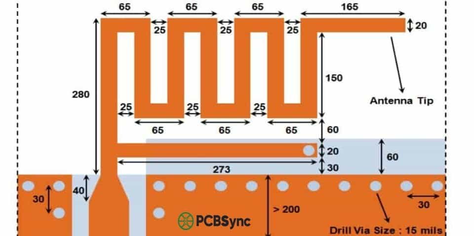
The MIFA is a further evolution of the IFA where the horizontal element is folded in a zigzag pattern. It features very compact design, reduced efficiency compared to straight IFA, sensitivity to nearby components, and typical gain of 0.5-2 dBi. Best for wireless mice, presenters, BLE beacons, and ultra-compact wearables.
Patch (Microstrip) Antenna
Patch antennas consist of a flat rectangular or circular conductive element on one side of the PCB with a ground plane on the opposite side. They feature directional radiation, higher gain (4-8 dBi typical), narrow bandwidth, and larger footprint. Best for GPS receivers, automotive radar, satellite communications, and directional links.
Loop Antenna
Loop antennas form a closed conductive path, sensitive to magnetic fields. They’re very compact for low frequencies, often require a resonating capacitor, and have typical gain of -2 to 1 dBi. Best for NFC, RFID readers/tags, AM radio, and magnetic field sensors.
PCB Antenna Comparison Table
Antenna Type
Size
Bandwidth
Gain (dBi)
Ground Plane
Complexity
Best For
Monopole
Medium
Medium
1-3
Yes
Low
General IoT
Dipole
Large
Medium
2-3
Partial
Low
Wi-Fi AP
IFA
Small
Medium
1-2.5
Yes
Medium
Smartphones
MIFA
Very Small
Narrow
0.5-2
Yes
Medium
Wearables
Patch
Large
Narrow
4-8
Yes
Medium
GPS, Radar
Loop
Very Small
Narrow
-2 to 1
No
Low
NFC, RFID
PCB Antenna Design Calculations
Now let’s get into the math. I’ll walk you through the essential calculations with practical examples.
Step 1: Determine the Operating Frequency
Your target frequency determines nearly everything else. Common ISM bands include:
Band
Frequency
Common Applications
Sub-1 GHz
433, 868, 915 MHz
LoRa, Zigbee, remotes
2.4 GHz
2400-2483.5 MHz
Wi-Fi, Bluetooth, BLE
5 GHz
5150-5850 MHz
Wi-Fi 5/6, 5G NR
GPS L1
1575.42 MHz
GPS receivers
Step 2: Calculate the Wavelength
Using the basic formula, calculate the wavelength in free space. But electromagnetic waves travel slower in a PCB substrate than in free space. You need to account for the effective dielectric constant:
λ_eff = λ₀ / √εr_eff where εr_eff ≈ (εr + 1) / 2
For FR4 with εr = 4.4, εr_eff ≈ 2.7, so √εr_eff ≈ 1.64. A 2.4 GHz quarter-wave antenna on FR4: λ₀ = 125 mm, λ_eff = 76 mm, λ/4 ≈ 19 mm.
Antenna Length Reference Table
Frequency
λ₀ (Free)
λ/4 (Free)
λ/4 (FR4)
Typical Length
433 MHz
693 mm
173 mm
106 mm
100-110 mm
868 MHz
346 mm
86.5 mm
53 mm
50-55 mm
915 MHz
328 mm
82 mm
50 mm
47-52 mm
2.4 GHz
125 mm
31.25 mm
19 mm
18-20 mm
5.8 GHz
52 mm
13 mm
7.9 mm
7-8 mm
Note: Actual lengths vary based on substrate thickness, trace width, and proximity to components. Always verify with simulation.
PCB Antenna Layout Best Practices
After designing hundreds of wireless products, here are the layout rules I always follow.
Antenna Placement
Rule #1: Always place the antenna at the PCB edge or corner. This is probably the most important layout decision you’ll make. An antenna placed in the middle of a board, surrounded by ground plane and components, will perform terribly. The corner works best because it provides clearance in five spatial directions and maximum distance from noisy digital circuitry.
Rule #2: Extend the antenna beyond the main PCB if possible. Many successful designs (like the ESP32 modules) have the antenna portion extending past the main board outline. This gives maximum radiation freedom.
Keep-Out Zones and Clearance
Every antenna requires a copper-free zone around and below it. This applies to ALL layers of your PCB.
2.4 GHz antennas: Minimum 15 mm clearance from ground plane edge
Sub-1 GHz antennas: Minimum 20-30 mm clearance
Lateral clearance: 3-5 mm from antenna edges on all layers
Keep out of the clearance zone: all copper (traces, pours, vias), metal components (USB, shields), large passive components, batteries, LCDs, and mounting hardware.
Ground Plane Design
The ground plane is literally half of your antenna system. Use a solid, continuous ground plane (don’t slice it up with traces). For multi-layer boards, stitch the ground layers together with via fences along the edge. Keep the ground plane edge parallel to monopole antennas, and size the ground plane to at least λ/4 in the critical dimension.
50-Ohm Feed Line Design
The transmission line connecting your RF IC to the antenna must maintain 50-ohm characteristic impedance. Coplanar Waveguide with Ground (CPWG) is the preferred approach for most PCB antennas. For a typical 4-layer, 1.6 mm FR4 board with 1 oz copper: a 50-ohm microstrip is approximately 2.9 mm wide. Always use an impedance calculator to get exact dimensions for your stackup.
Common PCB Antenna Design Mistakes
I’ve made all of these mistakes at some point. Learn from my pain.
Mistake #1: Ignoring the Ground Plane
The most common mistake: designing a beautiful antenna, then placing it on a tiny evaluation board with an inadequate ground plane. The fix: Size your ground plane appropriately from the start. For sub-1 GHz, you need at least 80-100 mm of ground plane length.
Mistake #2: Copper in the Keep-Out Zone
Designers carefully create keep-out zones on the top layer, then route power traces right under the antenna on inner layers. The fix: Create keep-out zones that apply to ALL copper layers.
Mistake #3: Skipping Simulation
“It worked on the reference design” is famous last words. Your board isn’t the reference design. The fix: Simulate your specific layout with your enclosure and components using tools like HFSS or CST.
Mistake #4: Forgetting the Enclosure
An antenna that works perfectly on the bench may fail completely when mounted in a plastic enclosure. Plastic cases shift the resonant frequency downward (typically 50-200 MHz for 2.4 GHz antennas). The fix: Test with the final enclosure and leave room in your matching network to compensate.
Even well-designed antennas rarely hit exactly 50 ohms. Real-world factors like enclosure proximity, battery placement, and PCB manufacturing variations all shift the impedance. Understanding how to match your antenna is crucial for achieving optimal performance.
When You Need a Matching Network
You need impedance matching when your antenna’s measured impedance differs significantly from 50 ohms, your enclosure or nearby components detune the antenna, you’re using a chip antenna (almost always requires matching), or the antenna was designed for a different ground plane size. The general rule: if your return loss (S11) is worse than -10 dB across your operating band, you need matching.
Pi-Network and L-Network Matching
The Pi-network is the most common matching topology for PCB antennas—two shunt capacitors with a series inductor. It can match a wide range of impedances and offers filtering capability. The simpler L-network uses only two components and works well when impedance transformation isn’t too extreme (within 2:1 of 50 ohms).
Component Selection for RF Matching
Use high-Q ceramic capacitors (COG/NPO dielectric) and avoid X7R/Y5V which vary with frequency. Watch for self-resonant frequency (SRF). For inductors, use thin-film or multilayer chip types rather than wire-wound. Check Q-factor at your operating frequency. Typical 0402 components for 2.4 GHz: Murata GJM15 series capacitors, Murata LQW series inductors.
PCB Material Selection for Antenna Design
The choice of PCB substrate material significantly impacts antenna performance. While many designers default to FR4 for cost reasons, understanding when to use specialized materials can make the difference between a working product and one that fails certification.
FR4 vs High-Frequency Laminates
Standard FR4 is adequate for most applications up to about 3 GHz. Its dielectric constant (εr) ranges 4.2-4.5 with loss tangent of 0.02. The main challenge is consistency—εr can vary ±10% between batches. High-frequency laminates like Rogers RO4003C (εr: 3.38, tan δ: 0.0027) offer much better consistency and lower losses at 3-5× the cost. Consider upgrading when operating above 5 GHz, when efficiency requirements exceed 70%, or when manufacturing variation causes yield issues.
EMC and Regulatory Considerations
Designing a great antenna is only part of the challenge. Your product must also pass regulatory testing for the markets you’re targeting. FCC Part 15.247 covers spread spectrum devices (Wi-Fi, Bluetooth) in the US, while CE marking requires ETSI EN 300 328 for 2.4 GHz band in Europe.
Tips for passing regulatory testing:
Filter harmonics—even a perfect 2.4 GHz antenna radiates at 4.8 GHz and 7.2 GHz if your transmitter generates harmonics
Shield sensitive circuits and keep noisy digital circuits away from the antenna
Use proper grounding—poor ground design causes common-mode emissions
Design for -3 dB below regulatory limits to account for production variation
PCB Antenna Simulation and Testing
Simulation Software Options
Software
Vendor
Solver
Price
Learning
Ansys HFSS
Ansys
FEM
$$$$$
Steep
CST Studio
Dassault
FDTD/FEM
$$$$$
Moderate
FEKO
Altair
MoM
$$$$
Moderate
openEMS
Open Source
FDTD
Free
Steep
PCB Antenna Design Resources
Here are the resources I use regularly for PCB antenna design.
What is the difference between a chip antenna and a PCB antenna?
A chip antenna is a pre-manufactured, surface-mount component (usually ceramic) that you solder onto your PCB. A PCB antenna is etched directly into the copper layers of the PCB itself. Chip antennas are faster to implement but more expensive and cannot be tuned by changing dimensions. PCB antennas are cheaper, require more design expertise, and can be optimized for specific applications.
How do I calculate the length of a PCB antenna?
The basic formula for a quarter-wave monopole antenna is: L = (c / f) × (1 / 4) × (1 / √εr_eff). For 2.4 GHz on FR4 with εr_eff ≈ 2.7, L = (3 × 10⁸ / 2.4 × 10⁹) × 0.25 × (1 / 1.64) ≈ 19 mm. Always add 5-10% extra length to allow for trimming during tuning.
Why does my PCB antenna need a ground plane?
For monopole and IFA-type antennas, the ground plane acts as the second half of the antenna. It creates an “image” of the quarter-wave element, effectively forming a half-wave dipole. Without an adequate ground plane, resonant frequency shifts unpredictably, radiation efficiency drops significantly, and radiation pattern becomes distorted.
Can I use any PCB material for antenna design?
Technically yes, but material choice significantly affects performance. FR4 (standard PCB material) works fine for 2.4 GHz and below but has higher loss at 5 GHz and above. High-frequency laminates (Rogers, Taconic) offer lower loss and more consistent properties but are 3-10× more expensive. For most IoT and consumer electronics, standard FR4 works adequately up to 6 GHz.
How do I test a PCB antenna without expensive equipment?
While professional testing requires a VNA and anechoic chamber, you can do basic validation with: (1) NanoVNA – low-cost ($50-150) vector network analyzer for S11 measurement, (2) Range testing – measure actual communication distance, (3) Spectrum analyzer – check radiation frequency, (4) Comparison testing – test against a known-good reference antenna. For production validation, send samples to an antenna test lab (typical costs $500-2000).
Conclusion
Designing a successful PCB antenna requires balancing multiple factors: electrical performance, physical constraints, manufacturing cost, and real-world operating conditions. The key principles to remember: start with the right topology, size your ground plane appropriately, maintain proper keep-out zones, design for tunability, simulate before fabrication, and test in the actual enclosure.
PCB antenna design is one of those skills that improves dramatically with experience. Each project teaches you something new about the interplay between theory and practice. Don’t get discouraged if your first designs need multiple iterations—even experienced RF engineers rarely nail it on the first try.
The best PCB antenna designs come from engineers who understand both the electromagnetic fundamentals and the practical realities of manufacturing, cost, and system integration. Keep experimenting, keep measuring, and keep learning.
Inquire: Call 0086-755-23203480, or reach out via the form below/your sales contact to discuss our design, manufacturing, and assembly capabilities.
Quote: Email your PCB files to Sales@pcbsync.com (Preferred for large files) or submit online. We will contact you promptly. Please ensure your email is correct.
Notes: For PCB fabrication, we require PCB design file in Gerber RS-274X format (most preferred), *.PCB/DDB (Protel, inform your program version) format or *.BRD (Eagle) format. For PCB assembly, we require PCB design file in above mentioned format, drilling file and BOM. Click to download BOM template To avoid file missing, please include all files into one folder and compress it into .zip or .rar format.


