Inquire: Call 0086-755-23203480, or reach out via the form below/your sales contact to discuss our design, manufacturing, and assembly capabilities.
Quote: Email your PCB files to Sales@pcbsync.com (Preferred for large files) or submit online. We will contact you promptly. Please ensure your email is correct.
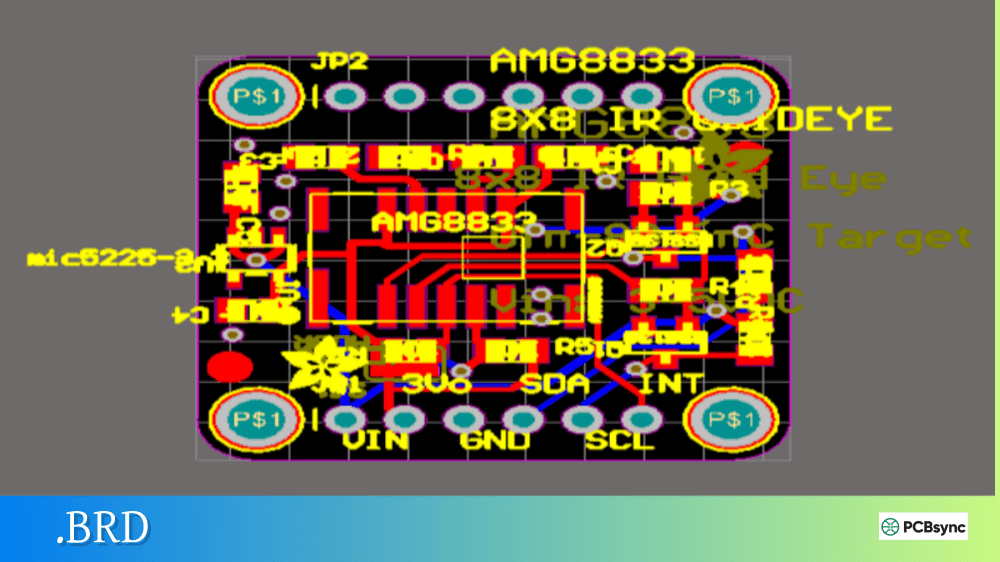
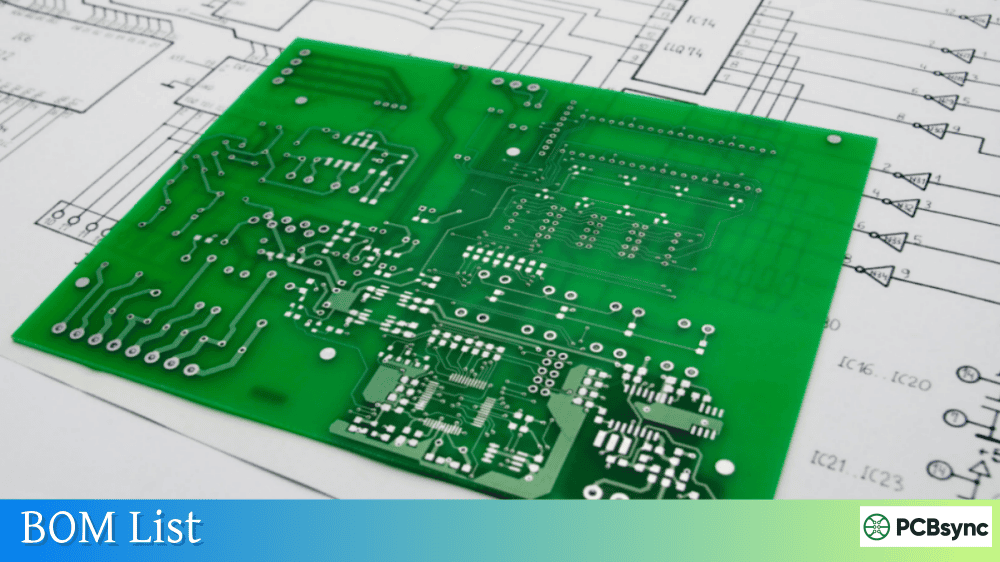
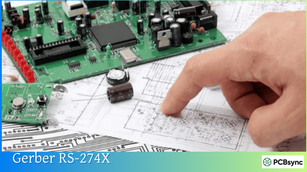
Notes: For PCB fabrication, we require PCB design file in Gerber RS-274X format (most preferred), *.PCB/DDB (Protel, inform your program version) format or *.BRD (Eagle) format. For PCB assembly, we require PCB design file in above mentioned format, drilling file and BOM. Click to download BOM template To avoid file missing, please include all files into one folder and compress it into .zip or .rar format.
What are PCB Panelization Files? Complete Array Format Guide
If you’ve ever wondered why your PCB manufacturer asks for “panelization files” or charges extra for “array setup,” you’re not alone. After years of optimizing production layouts and troubleshooting assembly line issues, I’ve learned that understanding panelization files can mean the difference between a cost-effective production run and an expensive mistake.
This guide covers everything you need to know about PCB panelization files, from basic concepts to the technical specifications that will help you maximize board yield and minimize manufacturing costs.
PCB panelization files are the design documents that define how multiple individual printed circuit boards are arranged on a larger manufacturing panel. These files contain all the information a fabricator needs to produce your boards in an array format, including board placement, spacing, separation methods, and the required tooling features.
When you submit your design to a manufacturer, you’re typically providing Gerber files for a single board. Panelization files take this further by specifying how many copies of your board (or multiple different boards) should be grouped together on a standard manufacturing panel. The result is an array—a collection of identical or mixed PCBs that travel through fabrication and assembly as a single unit before being separated into individual boards.
Why Panelization Files Matter for PCB Production
The electronics manufacturing process is designed around handling panels, not individual small boards. Pick-and-place machines, reflow ovens, and wave soldering equipment all work most efficiently with standardized panel sizes. Here’s what proper panelization files deliver:
Manufacturing Efficiency: Assembly equipment can populate dozens of boards simultaneously when they’re arranged in a panel. Without panelization, each small board would need individual handling, dramatically increasing production time.
Cost Reduction: More boards per panel means lower per-unit costs. The math is straightforward—if you can fit 20 boards on a panel instead of 15, you’ve just reduced your fabrication cost per board by roughly 25%.
Quality Control: Panels provide stable platforms during reflow soldering. Individual small boards can shift, twist, or even fall through conveyor gaps. Proper panelization maintains board rigidity throughout the assembly process.
Handling Protection: The rails and breakaway tabs in a panelized design protect delicate board edges and components from damage during manufacturing and shipping.
Types of PCB Panelization Files
Depending on your manufacturer and design software, you may encounter several file formats used to communicate panel specifications.
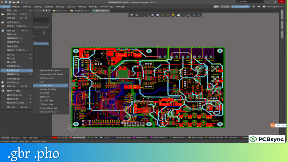
Standard Gerber-Based Panelization Files
The most common approach involves creating a new set of Gerber files that represent the entire panel rather than a single board. This panel Gerber package includes:
File Type
Description
Extension
Panel Copper Layers
All copper layers repeated in array pattern
.GTL, .GBL, .G1, .G2
Panel Solder Mask
Mask layers for entire array
.GTS, .GBS
Panel Silkscreen
Legend/overlay for full panel
.GTO, .GBO
Panel Outline
Mechanical layer showing full array boundary
.GKO, .GM1
Panel Drill File
All hole data for complete array
.DRL, .XLN
V-Score Layer
Lines indicating V-groove locations
.GM2, .GML
Routing Layer
Tab and routing path definitions
.GML
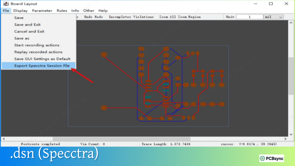
CAD Software Native Panel Files
Modern PCB design tools include built-in panelization features that generate panel-specific files:
Altium Designer: Uses the Embedded Board Array feature to create panel .PcbDoc files that can be exported to Gerber.
KiCad: The KiKit plugin or manual panel creation generates standard Gerber outputs for the complete array.
EAGLE: Panelization through ULP scripts or CAM processor configurations.
EasyEDA: Built-in panelization tools that output manufacturer-ready files.
Panel Drawing and Specification Files
Beyond Gerber data, comprehensive panelization files often include:
Document Type
Purpose
Typical Format
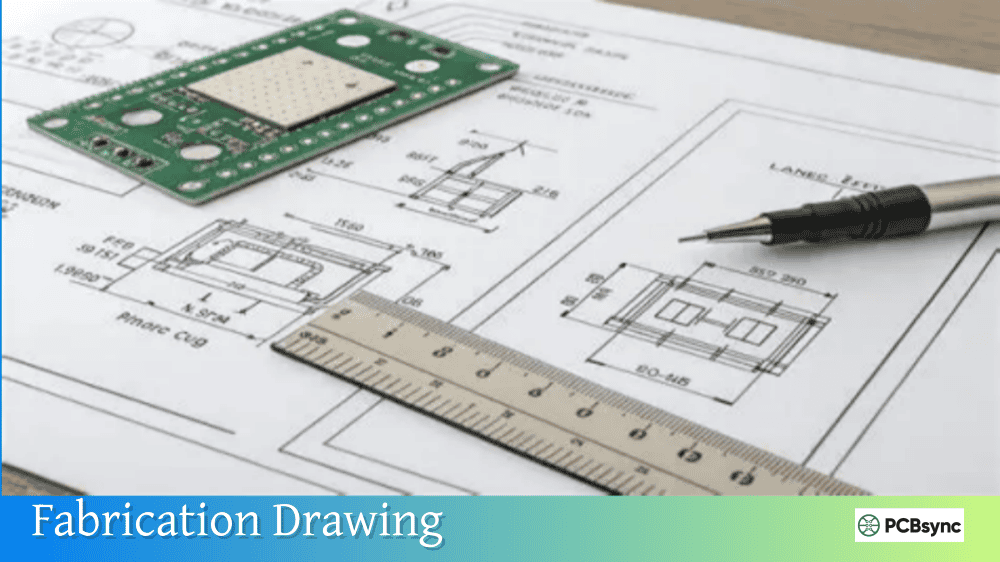
Panel Drawing
Dimensioned layout showing all features
PDF, DXF
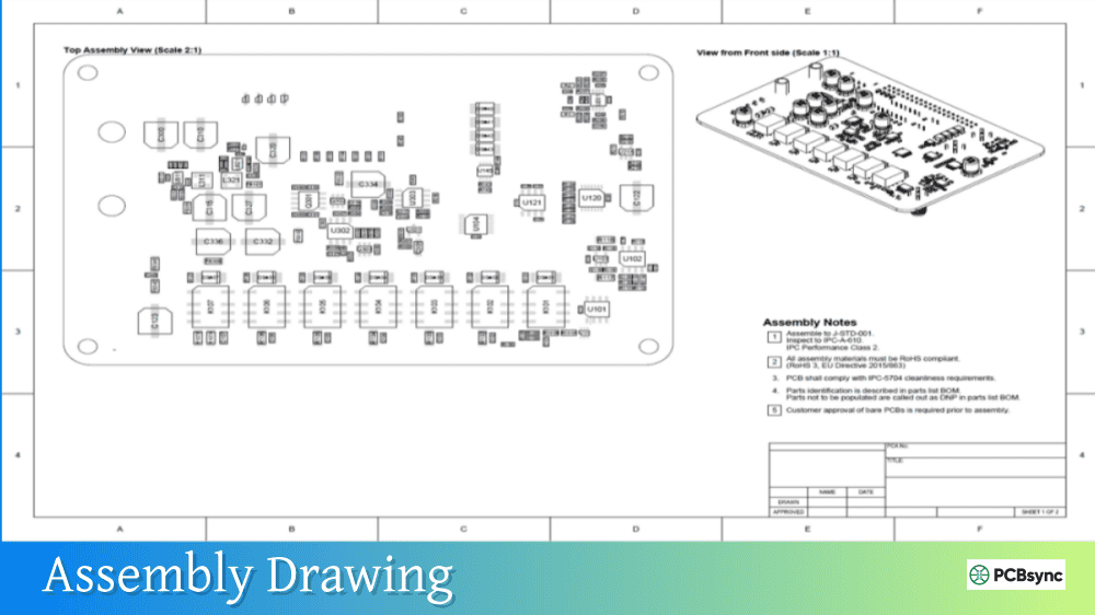
Assembly Drawing
Component placement relative to panel
PDF
Fabrication Notes
Special instructions for V-score depth, routing, etc.
PDF, TXT
Pick-and-Place File
Component coordinates referenced to panel origin
CSV, TXT
BOM
Bill of materials for panelized quantity
CSV, XLS
Panel Design Methods and Separation Techniques
The way boards connect within a panel directly impacts how they’ll be separated after assembly. Your panelization files must specify which method you’re using.
V-Groove (V-Score) Panelization
V-groove panelization involves cutting V-shaped channels partially through the panel material from both top and bottom surfaces. Each groove removes approximately one-third of the board thickness from each side, leaving a thin web of material (roughly one-third thickness) that holds the boards together.
V-Score Specifications for Panelization Files:
Parameter
Typical Value
Notes
Groove Angle
30° or 45°
Check manufacturer capability
Remaining Web
0.15mm – 0.4mm
Depends on board thickness
Minimum Board Thickness
1.0mm
Thinner boards may flex too much
Edge Clearance
0.5mm minimum
Keep copper/components away from score line
V-scoring works best for rectangular boards where score lines run straight across the entire panel. The boards separate cleanly with a slight bending motion or a scoring machine.
When to Use V-Scoring:
Square or rectangular board shapes
Components don’t hang over board edges
Board thickness ≥1.0mm
You need clean, smooth edges after separation
Tab Routing with Mouse Bites
When V-scoring isn’t feasible—typically due to irregular board shapes or edge-mounted components—tab routing with perforated breakaway tabs (mouse bites) provides an alternative.
Mouse bites are rows of small holes drilled into tabs that connect individual boards. After assembly, boards snap apart along these perforations, leaving small protrusions that may require sanding.
Mouse Bite Specifications:
Parameter
Typical Value
Notes
Hole Diameter
0.5mm (20 mil)
Most common size
Hole Spacing
0.75mm – 1.0mm center-to-center
Closer = easier break
Tab Width
3mm – 5mm
Wider = stronger during handling
Tab Spacing
50mm – 75mm along edge
More tabs = better support
Edge Clearance
3mm minimum
Keep components away from tabs
When to Use Mouse Bites:
Irregular or rounded board shapes
Components near or overhanging board edges
Mixed board designs in one panel
Hand-separation is acceptable
Solid Tab Panelization
Some designs use solid tabs without perforations for maximum panel strength during manufacturing. These require specialized depaneling equipment:
Router depaneling: CNC routing cuts boards from panel
Laser cutting: Precise cuts without mechanical stress
Blade tools: Hook-shaped cutters for manual separation
Solid tabs add cost and complexity but provide the strongest panel structure for heavy component loads or demanding assembly processes.
Essential Panel Features for Assembly
Your panelization files must include certain features to ensure compatibility with automated assembly equipment.
Tooling Holes
Tooling holes allow the panel to be precisely fixed in assembly fixtures and test equipment. Standard specifications:
Feature
Specification
Hole Diameter
3.2mm (0.126″) or 4.0mm (0.156″)
Location
Panel corners, 6.35mm (0.250″) from edges
Quantity
Minimum 3 holes, typically 4
Plating
Non-plated (NPTH)
Tolerance
±0.05mm
Fiducial Marks
Fiducial marks are reference points that allow pick-and-place machines to precisely align component placement. They appear as exposed copper circles surrounded by solder mask clearance.
Panel Fiducial Requirements:
Parameter
Specification
Diameter
1.0mm copper pad
Clearance
2.0mm – 3.0mm solder mask opening
Location
Minimum 3 per panel (diagonal corners)
Edge Distance
≥4mm from panel edge
Placement
Rails/borders, plus individual boards for fine-pitch components
Rails and Borders
Rails are the border areas surrounding your board array. They provide handling area and house tooling holes and fiducials without interfering with the actual PCB designs.
Rail Specification
Typical Value
Rail Width
5mm – 10mm minimum
Position
Two opposing sides (minimum) or all four sides
Material
Same as PCB substrate
Features
Tooling holes, fiducials, text markings
Creating Panelization Files in Popular CAD Tools
Let me walk you through the basic process for the tools I use most frequently.
Panelization in Altium Designer
Altium’s Embedded Board Array feature handles most panelization tasks:
Create a new PCB document sized for your panel dimensions
Navigate to Place → Embedded Board Array/Panelize
Select your source .PcbDoc file
Define row and column count, spacing parameters
Add rails with tooling holes and fiducials
Define V-score lines on a mechanical layer or add mouse bite patterns
Export complete Gerber package including all layers
Panelization in KiCad
KiCad doesn’t have native panelization, but the KiKit plugin provides excellent functionality:
Install KiKit via pip: pip install kikit
Create a panel configuration file (JSON or CLI parameters)
Define board repetition, spacing, tabs/V-cuts
Generate panelized PCB file
Export Gerbers from the panel design
Alternatively, manual panelization involves copying and arranging board elements in a new PCB file.
Using Manufacturer Panelization Services
Most PCB manufacturers offer panelization as a service. You provide single-board Gerbers, and they create the panel. This approach works well but has considerations:
Advantages:
No panel design work required
Manufacturer optimizes for their processes
Often included in assembly pricing
Disadvantages:
Less control over panel layout
May not optimize board count for your specific needs
Impedance variation: Critical RF traces may behave differently with grain orientation changes.
Calculating Board Yield
Use this approach to estimate boards per panel:
Start with panel usable area (total size minus borders)
Calculate board footprint including spacing and any rail requirements
Try both orientations
Account for partial board spaces that can’t be used
Many manufacturers provide online calculators, or you can use tools like KwickFit to optimize layouts before committing to a design.
Common Panelization Mistakes to Avoid
After reviewing hundreds of panel designs, these are the issues I see most frequently:
Insufficient Edge Clearance: Components too close to board edges get damaged during depaneling. Maintain at least 3mm clearance from any separation line.
Missing Fiducials: Without proper fiducials, placement machines can’t align accurately. Always include panel-level and board-level fiducials for fine-pitch components.
Wrong V-Score Depth: Specifying improper score depth leads to boards that won’t separate (too shallow) or break during handling (too deep). Let your manufacturer determine depth based on your board thickness.
Incompatible Separation Methods: Mixing V-scores and routed edges on the same board side creates manufacturing complications. Use one method consistently where possible.
Ignoring Component Overhang: Parts that extend beyond board edges need tab routing, not V-scoring. Check your 3D model before selecting separation method.
IPC-7351: Generic Requirements for Surface Mount Design
IPC-2221: Generic Standard on Printed Board Design
IPC-A-610: Acceptability of Electronic Assemblies
Frequently Asked Questions About Panelization Files
What’s the difference between a panel and an array?
In PCB terminology, these terms are often used interchangeably, but there’s a subtle distinction. A “panel” typically refers to the full manufacturing substrate including borders and rails, while an “array” specifically describes the repeated arrangement of individual PCBs within that panel. When you create panelization files, you’re defining the complete panel, which contains your board array.
Can I put different PCB designs on the same panel?
Yes, this is called mixed panelization or multi-design panelization. However, all boards must share identical specifications: same layer count, same thickness, same surface finish, and same copper weight. If any parameter differs, the boards cannot be processed together. Mixed panels are common when you have several small designs that would otherwise waste panel space.
Should I create my own panelization files or let the manufacturer do it?
For prototypes and small production runs, letting the manufacturer handle panelization is usually the most practical choice. They’ll optimize for their equipment and processes. However, for high-volume production where per-unit cost is critical, creating your own panelization files gives you control over board count optimization and ensures the layout meets your specific assembly requirements.
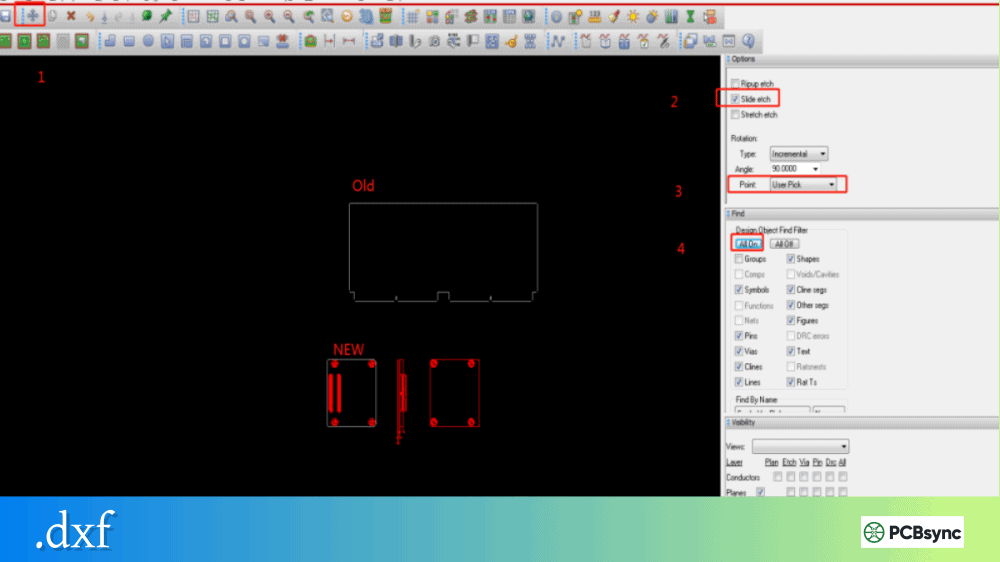
How do I specify V-groove locations in my panelization files?
V-groove locations should be indicated on a dedicated mechanical layer in your Gerber output. Draw lines where you want the grooves to run—these must extend completely across the panel in straight lines. Include a fabrication note specifying the groove angle (typically 30° or 45°) and let the manufacturer determine appropriate depth based on your board thickness. Some manufacturers prefer a separate DXF file for scoring specifications.
What panel size should I request for my project?
Ask your manufacturer which panel sizes they run and what border spacing they require. Then calculate how many boards fit on each available panel size, accounting for spacing between boards (typically 2-3mm for routing, 0mm for V-scoring) and rail widths. Choose the panel size that yields the highest board count for your order quantity. For smaller orders, manufacturers often pool multiple customers’ boards on shared panels to reduce costs.
Final Thoughts on Panelization Files
Getting panelization right isn’t glamorous work, but it’s one of those fundamentals that separates efficient production from costly delays. The time you invest in understanding panel requirements, selecting appropriate separation methods, and creating proper panelization files pays off in lower manufacturing costs, smoother assembly runs, and fewer quality issues.
Start by consulting your manufacturer early in the design process. They can provide specific guidelines for their equipment and may offer panelization as a service. If you’re handling panelization yourself, use the specifications in this guide as a starting point, but always verify requirements with your fab house.
Remember that panelization isn’t just about fitting more boards on a panel—it’s about creating a manufacturable design that flows smoothly through fabrication, assembly, and test. Get the panel design right, and everything downstream becomes easier.
Inquire: Call 0086-755-23203480, or reach out via the form below/your sales contact to discuss our design, manufacturing, and assembly capabilities.
Quote: Email your PCB files to Sales@pcbsync.com (Preferred for large files) or submit online. We will contact you promptly. Please ensure your email is correct.
Notes: For PCB fabrication, we require PCB design file in Gerber RS-274X format (most preferred), *.PCB/DDB (Protel, inform your program version) format or *.BRD (Eagle) format. For PCB assembly, we require PCB design file in above mentioned format, drilling file and BOM. Click to download BOM template To avoid file missing, please include all files into one folder and compress it into .zip or .rar format.


