Inquire: Call 0086-755-23203480, or reach out via the form below/your sales contact to discuss our design, manufacturing, and assembly capabilities.
Quote: Email your PCB files to Sales@pcbsync.com (Preferred for large files) or submit online. We will contact you promptly. Please ensure your email is correct.
Notes: For PCB fabrication, we require PCB design file in Gerber RS-274X format (most preferred), *.PCB/DDB (Protel, inform your program version) format or *.BRD (Eagle) format. For PCB assembly, we require PCB design file in above mentioned format, drilling file and BOM. Click to download BOM template To avoid file missing, please include all files into one folder and compress it into .zip or .rar format.
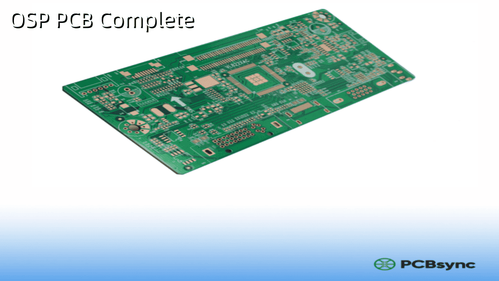
If you’ve worked in PCB manufacturing for any length of time, you’ve probably encountered the question: which surface finish should I use? After spending over a decade in the industry troubleshooting soldering issues and optimizing production lines, I can tell you that the answer depends heavily on your specific application. But there’s one finish that keeps coming up in cost-sensitive, high-volume projects: OSP PCB surface finish.
OSP, which stands for Organic Solderability Preservative, is a water-based organic compound applied to exposed copper pads on printed circuit boards. Unlike metallic finishes such as HASL or ENIG, OSP creates a thin, transparent protective layer that prevents copper oxidation while maintaining excellent solderability. The coating typically measures just 0.2 to 0.5 microns—so thin you can barely see it—yet it plays a critical role in protecting your copper until assembly.
In this comprehensive guide, I’ll walk you through everything you need to know about OSP PCB surface finish: how the process works, when to use it (and when to avoid it), how it compares to alternatives like HASL and ENIG, and practical tips for getting the best results. Whether you’re designing consumer electronics, working on automotive applications, or just trying to cut costs without sacrificing quality, this guide has you covered.
Let me put it simply: copper oxidizes. Leave a bare copper PCB exposed to air for even a few days, and you’ll start seeing tarnish that makes soldering difficult or impossible. OSP solves this problem by applying a protective organic film that acts as a barrier between the copper and the atmosphere.
The OSP coating belongs to a class of organic compounds known as the azole family, including benzotriazoles, imidazoles, and benzimidazoles. When these compounds contact copper, they form a coordination bond with the metal surface, creating a thin but effective protective layer. During reflow soldering, the flux in your solder paste breaks down this organic layer, exposing clean copper that bonds readily with the molten solder.
Here’s what makes OSP unique compared to other finishes:
Organic composition: No metals involved, making it inherently lead-free and RoHS compliant
Extremely thin: 0.2–0.5 microns versus 3–6 microns for ENIG
Transparent appearance: The copper shows through, giving boards a distinctive look
Self-removing during soldering: The flux does the work—no separate removal step needed
Flat surface: Perfect for fine-pitch components and BGAs
How the OSP PCB Manufacturing Process Works
The OSP application process is straightforward compared to metallic finishes, which is one reason it’s so cost-effective. I’ve visited dozens of fabrication facilities, and the OSP line is always one of the simplest setups on the floor. Here’s the step-by-step breakdown:
Step 1: Cleaning and Surface Preparation
Before applying any surface finish, the copper must be absolutely clean. Contamination from oils, fingerprints, or oxidation will cause the OSP to apply unevenly. Most fabricators use an alkaline cleaning solution followed by a thorough rinse. This step is critical—I’ve seen entire batches fail ICT testing because of inadequate cleaning before OSP application.
Step 2: Micro-Etching
The cleaned boards go through a micro-etching process that removes a thin layer of copper (typically 1.0–1.5 µm per minute) and creates a slightly roughened surface. This roughening dramatically improves the adhesion between the copper and the OSP compound. Think of it like sanding wood before painting—the texture helps the coating stick.
Step 3: Rinsing with Deionized Water
After micro-etching, the boards are rinsed with DI (deionized) water. Using DI water is essential here—regular water contains ions that can contaminate the OSP solution and cause tarnishing after reflow. The pH of the rinse water should be maintained between 4.0 and 7.0 to prevent damage to the developing OSP layer.
Step 4: OSP Application
The boards are immersed in or sprayed with the OSP solution, which is typically maintained at a specific temperature and concentration. The organic compound bonds with the copper surface through adsorption, forming the protective film. Film thickness depends on immersion time, solution concentration, and temperature—all carefully controlled variables.
Step 5: Final Rinse and Drying
Another DI water rinse removes any excess OSP solution, followed by hot air drying. The boards then undergo quality inspection, including thickness measurement and visual checks. Once approved, they’re vacuum-packed with desiccants to protect them during storage and shipping.
Advantages of OSP PCB Surface Finish
Let me be direct: OSP isn’t the best finish for every application. But when it fits your requirements, it offers some compelling advantages that explain its widespread adoption.
Low Manufacturing Cost
OSP is the most economical surface finish available. The organic compounds are inexpensive, the equipment is simple, and the process is fast. In my experience, switching from ENIG to OSP can reduce surface finish costs by 30–40%—a significant savings on high-volume production runs. For consumer electronics with tight margins, this cost difference often determines project viability.
Environmentally Friendly
OSP uses water-based chemistry with no heavy metals. It’s inherently lead-free and compliant with RoHS, WEEE, and other environmental regulations. The process generates minimal waste compared to metallic plating operations. If sustainability is part of your company’s mandate, OSP checks all the boxes.
Excellent Surface Planarity
Unlike HASL, which creates uneven solder bumps, OSP produces an extremely flat surface. This flatness is essential for fine-pitch components (0.5mm pitch and below) and ball grid array (BGA) packages. If you’re working with dense SMT designs, OSP’s planarity can mean the difference between reliable placement and tombstoning issues.
Good Solderability
When the OSP layer is fresh and properly applied, it provides excellent wetting characteristics. The solder flows smoothly onto the exposed copper, creating strong, reliable joints. During reflow, the flux in your solder paste breaks down the OSP layer, exposing clean copper at exactly the right moment for optimal bonding.
Easy Rework and Reapplication
If the OSP coating gets damaged during handling or storage, it can be stripped and reapplied. This reworkability is a significant advantage over finishes like ENIG, where correcting problems is much more difficult and expensive. I’ve seen fabricators save entire batches by simply re-coating boards that were stored too long.
Every surface finish involves trade-offs, and OSP is no exception. Understanding these limitations is crucial for making the right choice.
Limited Shelf Life
This is OSP’s biggest drawback. The organic coating degrades over time, even under ideal storage conditions. Most manufacturers specify a shelf life of 6–12 months maximum, but I’ve seen solderability issues on boards stored for just 3 months in poor conditions. If your production schedule is unpredictable or you need to maintain large inventories, OSP may not be the right choice.
Sensitive to Handling
The thin OSP layer is easily damaged by fingerprints, scratches, or moisture exposure. Production operators must wear gloves, and boards require careful handling throughout the assembly process. I’ve audited facilities where poor handling practices caused significant quality issues that were initially blamed on the finish itself.
Limited Reflow Cycles
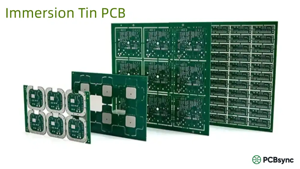
OSP can typically withstand only 4–6 reflow cycles before the coating degrades to the point of unreliable soldering. For double-sided assembly with mixed SMT and through-hole components, this limitation can become problematic. If your assembly process requires multiple thermal cycles, consider ENIG or immersion tin instead.
Difficult Visual Inspection
Because OSP is transparent, visual inspection for coating defects is challenging. You can’t easily see thin spots, contamination, or incomplete coverage. Most quality control programs rely on solderability testing and thickness measurement rather than visual inspection alone.
Not Ideal for Plated Through-Holes
OSP doesn’t provide the same level of protection inside plated through-holes as it does on surface pads. For designs with significant PTH components, especially those requiring wave soldering, you may need to consider alternative finishes or selective OSP application.
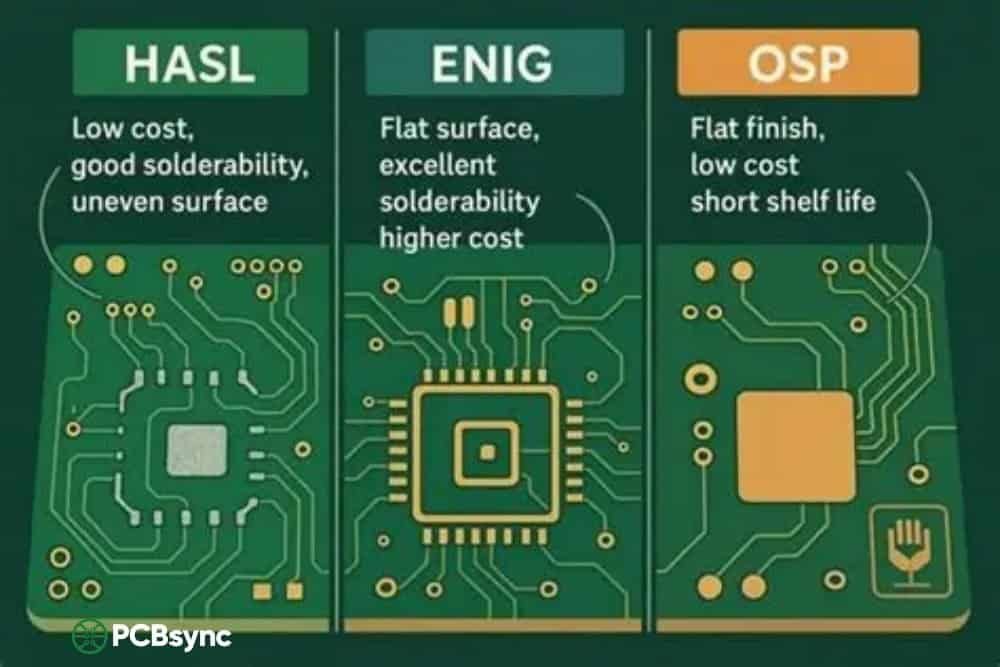
OSP vs. HASL vs. ENIG: Comparison Table
Choosing between surface finishes requires weighing multiple factors. Here’s a practical comparison based on real-world performance:
Parameter
OSP
HASL (Lead-Free)
ENIG
Cost
Lowest
Low
Highest
Shelf Life
6–12 months
12+ months
12+ months
Surface Flatness
Excellent
Poor (uneven)
Excellent
Fine-Pitch Components
Suitable
Not suitable
Best choice
Reflow Cycles
4–6 cycles
6+ cycles
6+ cycles
RoHS Compliant
Yes
Yes (lead-free only)
Yes
Coating Thickness
0.2–0.5 µm
1–25 µm
3–6 µm (Ni) + 0.05–0.1 µm (Au)
Wire Bonding
Not suitable
Not suitable
Suitable
Best For
High-volume consumer electronics, short turnaround
Based on my experience, OSP makes sense in these scenarios:
Consumer Electronics and High-Volume Production
Smartphones, tablets, wearables, home appliances—these products typically have short lifecycles, predictable production schedules, and tight cost targets. OSP’s low cost and flat surface make it ideal for the dense SMT assemblies common in consumer electronics. If you’re building millions of units per year, the cost savings add up quickly.
Prototyping and Quick-Turn Projects
When you need boards fast and plan to assemble them immediately, OSP is often the best choice. The simple process means shorter lead times, and the cost savings leave more budget for iteration. I’ve used OSP extensively for prototype runs where boards go straight from fabrication to assembly.
Products with Short Shelf Life Requirements
If your production schedule is well-controlled and boards will be assembled within a few months of fabrication, OSP’s shelf life limitation becomes irrelevant. Many contract manufacturers maintain just-in-time delivery systems where OSP works perfectly.
Fine-Pitch and BGA Applications
For designs with tight-pitch components (0.5mm and below), OSP’s excellent planarity provides consistent pad geometry that HASL simply cannot match. Combined with ENIG for gold fingers or selective applications, OSP can handle even demanding SMT requirements.
When to Avoid OSP PCB Finish
OSP isn’t appropriate for every application. Consider alternatives if:
Long storage requirements: If boards may sit in inventory for more than 6 months, choose ENIG or immersion tin
Multiple reflow cycles: Complex assemblies requiring many thermal cycles need more robust finishes
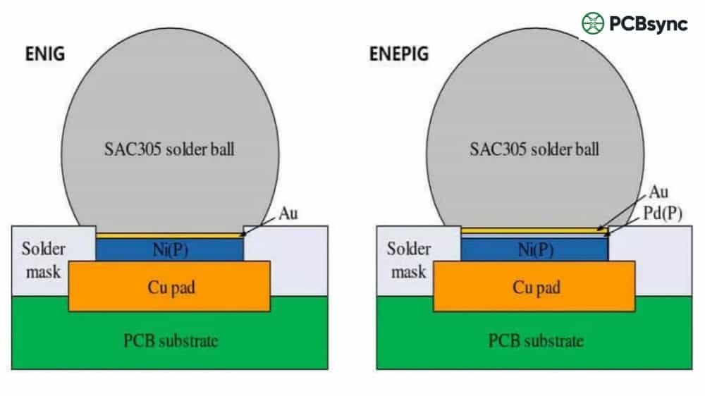
Wire bonding: OSP doesn’t support wire bonding—use ENIG or ENEPIG instead
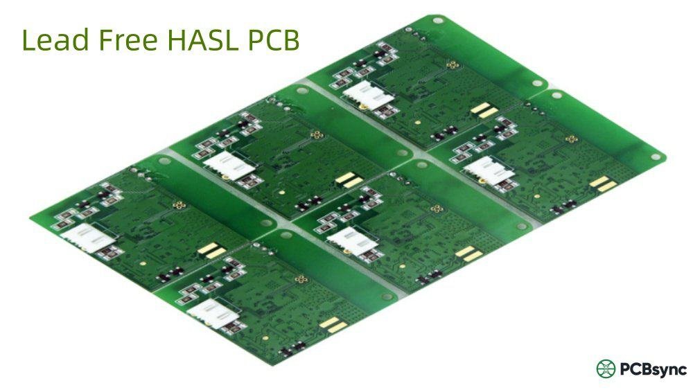
Heavy PTH content: Wave soldering and through-hole components work better with HASL
ICT testing requirements: OSP provides lower contact reliability for in-circuit test probes compared to metallic finishes
Storage and Handling Requirements for OSP PCBs
Proper storage is critical with OSP. I can’t stress this enough—I’ve seen quality issues on nearly every audit where storage conditions weren’t properly controlled. Follow these guidelines:
Parameter
Requirement
Temperature
15–30°C (59–86°F)
Relative Humidity
30–60% RH
Packaging
Vacuum-sealed with desiccant and humidity indicator card
Maximum Storage Time
6–12 months (shorter in humid environments)
After Opening Package
Complete SMT within 8–12 hours
Handling
Always wear gloves; avoid touching pad surfaces
Baking
NOT recommended—baking damages OSP coating
Important: Unlike moisture-sensitive components, OSP boards should NOT be baked before assembly. High temperatures will degrade or destroy the organic coating, defeating its purpose.
Relevant IPC Standards for OSP
When specifying OSP on your PCB documentation, reference these IPC standards:
IPC-4555: Performance Specification for Organic Solderability Preservative (OSP) Coating
IPC-6012: Qualification and Performance Specification for Rigid Printed Boards
IPC-J-STD-003: Solderability Tests for Printed Boards
IPC-TM-650, Method 2.4.14: Visual Examination of OSP Coatings
Note: IPC-4555 was developed to establish consistent quality standards for OSP, though reaching industry consensus on specific thickness requirements proved challenging due to the variety of OSP chemistries available.
Practical Tips for Working with OSP PCBs
Based on years of troubleshooting OSP-related issues, here are actionable recommendations:
Plan your production schedule: Order OSP boards only when you have a firm assembly date. Avoid building inventory.
Inspect incoming boards: Check vacuum seal integrity, humidity indicator status, and perform visual inspection before releasing to production.
Minimize exposure time: Open vacuum packages only when boards are ready for immediate assembly. Don’t open multiple panels at once.
Use appropriate flux: Choose solder paste and flux specifically designed for OSP surfaces. Aggressive fluxes can damage the coating before reflow.
Optimize reflow profile: OSP typically allows peak temperatures 2–5°C lower than other finishes. Work with your paste supplier to optimize.
Complete both sides quickly: For double-sided SMT, finish the second side within 12 hours of completing the first.
Handle misprints carefully: If solder paste printing fails, clean with 75% alcohol and a non-woven wipe—never IPA or aggressive solvents. Complete rework within 1 hour.
Consider selective finishes: For boards with gold fingers or edge connectors, use OSP for SMT pads and ENIG selectively where needed.
Useful Resources and References
For further reading and specifications, I recommend these resources:
1. Is OSP PCB finish lead-free and RoHS compliant?
Yes, OSP is inherently lead-free because it uses organic compounds rather than metallic materials. It’s fully compliant with RoHS (Restriction of Hazardous Substances), WEEE (Waste Electrical and Electronic Equipment), and other environmental regulations. This makes OSP one of the most environmentally friendly surface finish options available.
2. How many reflow cycles can OSP withstand?
OSP typically survives 4–6 reflow cycles under optimal conditions. Each thermal cycle degrades the organic coating slightly. For single-sided SMT assembly, this is rarely an issue. However, if your process involves multiple reflows (double-sided SMT plus wave soldering, rework, etc.), consider ENIG or another more robust finish.
3. Can I use OSP and ENIG on the same PCB?
Absolutely. Selective surface finishes are common for complex designs. You might use ENIG for gold fingers, edge connectors, or areas requiring wire bonding, while using OSP for standard SMT pads to reduce cost. Most PCB fabricators offer this selective finishing capability—just specify clearly in your fabrication notes.
4. What is the typical thickness of OSP coating?
OSP coating thickness ranges from 0.2 to 0.5 microns (200–500 nanometers), depending on the specific OSP chemistry used. Benzotriazole-based coatings tend to be thinner, while imidazole-based products produce slightly thicker films. The optimal thickness balances adequate protection against ease of flux penetration during soldering.
5. Why does my OSP board change color after soldering?
Color changes on OSP boards after reflow are common and usually indicate one of several conditions: variation in original coating thickness, differences in micro-etching depth, multiple reflow exposures, or surface contamination. In most cases, if soldering performance remains acceptable, the color change is cosmetic. However, significant discoloration may warrant investigation into process controls.
Conclusion
OSP PCB surface finish occupies an important niche in the PCB manufacturing landscape. It’s not the most durable option, and it requires careful handling and timely assembly. But for the right applications—high-volume consumer electronics, cost-sensitive projects, fine-pitch assemblies, and quick-turn production—OSP delivers excellent value.
The key to success with OSP is understanding its limitations and planning accordingly. Coordinate with your fabricator on lead times, maintain proper storage conditions, and ensure your assembly line is ready when boards arrive. When these elements align, OSP provides reliable, cost-effective performance that’s hard to beat.
As environmental regulations continue to tighten and surface mount technology pushes toward ever-smaller pitches, OSP’s combination of eco-friendliness, planarity, and low cost positions it as a surface finish that will remain relevant for years to come. Whether you’re an engineer selecting your first surface finish or a procurement specialist looking to optimize costs, understanding OSP helps you make better decisions for your PCB projects.
Inquire: Call 0086-755-23203480, or reach out via the form below/your sales contact to discuss our design, manufacturing, and assembly capabilities.
Quote: Email your PCB files to Sales@pcbsync.com (Preferred for large files) or submit online. We will contact you promptly. Please ensure your email is correct.
Notes: For PCB fabrication, we require PCB design file in Gerber RS-274X format (most preferred), *.PCB/DDB (Protel, inform your program version) format or *.BRD (Eagle) format. For PCB assembly, we require PCB design file in above mentioned format, drilling file and BOM. Click to download BOM template To avoid file missing, please include all files into one folder and compress it into .zip or .rar format.


