Inquire: Call 0086-755-23203480, or reach out via the form below/your sales contact to discuss our design, manufacturing, and assembly capabilities.
Quote: Email your PCB files to Sales@pcbsync.com (Preferred for large files) or submit online. We will contact you promptly. Please ensure your email is correct.
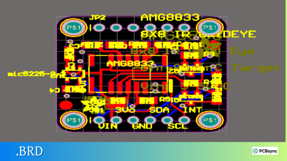
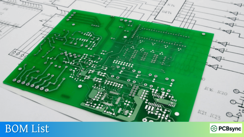
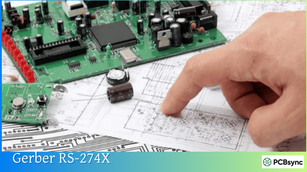
Notes: For PCB fabrication, we require PCB design file in Gerber RS-274X format (most preferred), *.PCB/DDB (Protel, inform your program version) format or *.BRD (Eagle) format. For PCB assembly, we require PCB design file in above mentioned format, drilling file and BOM. Click to download BOM template To avoid file missing, please include all files into one folder and compress it into .zip or .rar format.
What is ODB++? Complete PCB Data Exchange Format Guide
Every PCB designer eventually faces the same frustration: sending a dozen different files to the fabricator and hoping nothing gets lost or misinterpreted. Gerber files for each layer, drill files, netlists, pick-and-place data, BOMs—the list grows with board complexity. This is where ODB++ changes everything.
I remember the first time I sent an ODB++ file to a manufacturer. Instead of the usual back-and-forth emails clarifying layer stackups and drill specifications, the board went straight to production. That single experience converted me from a skeptic to an advocate. This guide explains what ODB++ is, how it works, and why it might be the right choice for your next project.
ODB++ (Open Database) is a comprehensive CAD-to-CAM data exchange format designed specifically for PCB design and manufacturing. Unlike Gerber, which requires multiple separate files to describe a complete board, ODB++ consolidates all fabrication, assembly, and test information into a single hierarchical database structure.
The file format was originally developed by Valor Computerized Systems in 1992 and released in 1995. The “++” suffix was added in 1997 when component descriptions were incorporated—a naming convention that echoes C++ programming. Mentor Graphics acquired Valor in 2010, and Siemens subsequently acquired Mentor in 2016. Today, Siemens continues to maintain and develop the ODB++ specification.
Despite its proprietary origins, ODB++ has become a de facto industry standard. The specification is freely available, and virtually all major PCB design tools support ODB++ export. Fabricators estimate that processing an 8-layer board with ODB++ takes approximately one hour, compared to up to five hours with traditional Gerber files.
In 2008, IPC approved ODB++ as an official standard for PCB data exchange, further cementing its position in the industry. The format continues to evolve with regular updates—version 8.1 was released in 2020—to address emerging manufacturing requirements and Industry 4.0 integration needs.
The ODB++ Family of Formats
In 2020, the ODB++ format was expanded and reorganized into what Siemens calls the ODB++ Family. This family consists of three connected formats that cover the complete design-to-manufacturing workflow:
Format
Purpose
Use Case
ODB++Design
Primary design data
DFM analysis, fabrication, assembly, test
ODB++Process
Machine-ready data
Converting design data for production equipment
ODB++Manufacturing
Shop floor communication
Industry 4.0 integration, machine-to-machine communication
ODB++Design
This is the format most designers work with. ODB++Design contains all the information generated by EDA tools and serves as the single carrier of design data from concept through manufacturing. It supports Design for Manufacturability (DFM), Design for Assembly (DFA), and Design for Test (DFT) analysis.
ODB++Process
ODB++Process acts as a translator between design intent and manufacturing reality. It converts ODB++Design data into formats that specific production equipment can consume—pick-and-place machines, automated optical inspection (AOI) systems, test fixtures, and more.
ODB++Manufacturing
The newest addition to the family, ODB++Manufacturing enables real-time communication between factory floor equipment and Industry 4.0 software systems. It supports the digital twin concept, allowing manufacturers to track production status and quality metrics throughout the manufacturing process.
ODB++ File Structure and Hierarchy
Unlike Gerber’s flat file structure, ODB++ uses a hierarchical folder organization that mirrors how PCB data is actually used. Understanding this structure helps when troubleshooting issues or manually inspecting data.
Top-Level Structure
An ODB++ database is a directory tree, typically compressed into a single archive (using gzip or ZIP) for transmission:
Folder/File
Contents
matrix/
Layer stackup definition, layer types, order
steps/
Design step data, layer features, components
symbols/
Graphical symbol definitions
fonts/
Text font definitions
misc/
Miscellaneous information, attributes
input/
Format identification data
user/
User-defined custom data
The Matrix File
The matrix file is the heart of an ODB++ database. It defines:
This structured approach eliminates the guesswork that plagues Gerber-based workflows, where fabricators must interpret layer order from file names or readme files.
Steps and Layers
Within the steps folder, each design step (typically representing a single PCB or panel) contains:
Layer feature files with copper patterns, pads, traces
Component placement data with reference designators
Netlist information for electrical connectivity
Profile data defining board outline
Drill tool definitions and hole locations
What ODB++ Contains That Gerber Doesn’t
The fundamental advantage of ODB++ lies in its comprehensive data coverage:
Data Type
ODB++
Gerber
Copper layers
✓
✓
Solder mask
✓
✓
Silkscreen
✓
✓
Drill data
✓
Separate Excellon file
Layer stackup
✓
README or drawing
Netlist
✓
Separate IPC-D-356 file
Component placement
✓
Separate pick-and-place file
Bill of materials
✓
Separate BOM file
Test points
✓
Separate file
Impedance requirements
✓
Notes or drawing
Material specifications
✓
Notes or drawing
This consolidation eliminates the primary source of manufacturing errors: mismatched or missing files in a multi-file submission.
ODB++ vs. Gerber vs. IPC-2581
Understanding how ODB++ compares to alternatives helps you choose the right format for your situation.
Comparison Table
Feature
Gerber RS-274X
Gerber X2/X3
ODB++
IPC-2581
File structure
Multiple files
Multiple files
Single archive
Single XML file
Netlist included
No
Optional
Yes
Yes
BOM included
No
No
Yes
Yes
Pick-and-place
No
X3 only
Yes
Yes
Layer stackup
Manual
Attributes
Automatic
Automatic
DFM capability
Limited
Better
Full
Full
Openness
Proprietary
Proprietary
Published spec
Open standard
Industry adoption
~90%
Growing
~30%
~5%
Setup time
Hours
Less
Minimal
Minimal
When to Use ODB++
ODB++ excels when:
Your fabricator supports it (most do)
You need complete design-to-manufacturing data transfer
Your design includes complex stackups or HDI features
You want automated DFM analysis
Assembly data must accompany fabrication data
When Gerber Might Be Better
Stick with Gerber when:
Your fabricator specifically requests it
You need maximum compatibility with any manufacturer
You’re concerned about IP protection (Gerber reveals less design intent)
Your board is simple and doesn’t require intelligent data transfer
How to Export ODB++ Files
Most modern PCB design tools support ODB++ export. Here’s the general process for major platforms.
Altium Designer
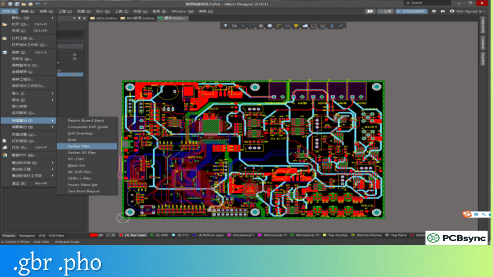
Open your PCB project
Go to File → Fabrication Outputs → ODB++ Files
Or create an Output Job file with ODB++ output
Configure layer mappings and options
Generate the output package
Altium creates a compressed .tgz or .zip file containing the complete ODB++ structure.
KiCad
As of KiCad 7, native ODB++ export is not available. However, you can use third-party plugins or convert Gerber/drill files to ODB++ using external tools.
OrCAD/Allegro
Open PCB Editor
Go to Manufacture → Export → ODB++
Configure the export settings
Select the destination folder
Generate the ODB++ database
PADS
Open your layout
Go to File → Export → ODB++
Set the output directory and options
Click Export
Working with ODB++ Viewers
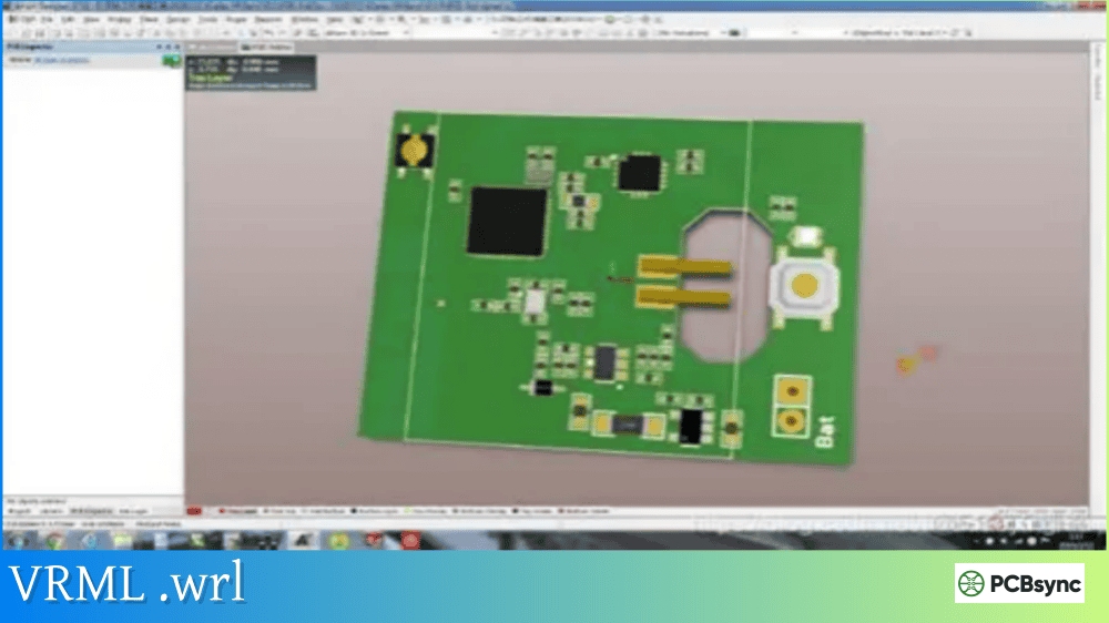
Before submitting ODB++ files to manufacturing, always verify them using a viewer.
Free ODB++ Viewer Options
Viewer
Source
Platform
Features
ODB++ Viewer
Siemens
Windows
Official viewer, full feature support
PCB Investigator
EasyLogix
Windows
Import/export, analysis tools
CAM350 (trial)
DownStream
Windows
Professional CAM features
The official ODB++ Viewer from Siemens (formerly Valor) is free to download and provides comprehensive visualization of all ODB++ data including layers, components, netlist, and attributes.
What to Check Before Submission
When reviewing your ODB++ export:
Verify layer count and order match your design
Confirm drill data includes all hole types (PTH, NPTH, blind, buried)
Check component placement data for assembly
Validate netlist connectivity
Review DFM analysis results if available
Advantages of Using ODB++
Reduced Manufacturing Errors
By consolidating all data into a single package, ODB++ eliminates the most common sources of fabrication errors. No more mismatched drill files, incorrect layer stackups, or missing assembly data.
Faster CAM Processing
Manufacturers report significant time savings when processing ODB++ compared to Gerber. The structured format allows CAM systems to automatically configure jobs without manual intervention.
Automated DFM Analysis
ODB++’s intelligent data structure enables automated Design for Manufacturability checks. CAM systems can identify potential issues—clearance violations, annular ring problems, acid traps—without manual inspection.
Complete Design Intent Communication
ODB++ conveys not just what to manufacture, but why. Attributes can specify controlled impedance requirements, surface finishes, material requirements, and other parameters that would otherwise require separate documentation.
Limitations and Considerations
Proprietary Format Concerns
Although the specification is published and freely available, ODB++ remains controlled by Siemens. Some companies prefer open standards like IPC-2581 to avoid potential vendor lock-in. The ODB++ Solutions Alliance exists to provide a forum for users and implementers, but ultimate control of the format remains with Siemens.
Intellectual Property Exposure
ODB++ files contain more design information than Gerber files, including netlist data and component specifications. Some designers are concerned this makes reverse engineering easier. However, fabricators need much of this information anyway, and ODB++ can be configured to limit exported data. The trade-off between manufacturing efficiency and IP protection is a decision each organization must make based on their specific circumstances.
Software Support Variations
While most major EDA tools export ODB++, implementation quality varies. Some tools produce better-structured ODB++ than others, and certain features may not export correctly depending on the source tool. Always verify exports in the official ODB++ viewer before production, and maintain communication with your fabricator about any tool-specific quirks they’ve observed.
ODB++ stands for Open Database. The “++” suffix was added in 1997 when component placement data was incorporated into the format, following the naming convention of the C++ programming language. Despite the “Open” name, ODB++ is a proprietary format controlled by Siemens, though the specification is freely published and implementation is unrestricted.
Is ODB++ better than Gerber?
ODB++ is more comprehensive than Gerber, containing netlist, BOM, and placement data that Gerber lacks. For complex boards requiring assembly, ODB++ reduces errors and processing time. However, Gerber remains more universally accepted, and some designers prefer its limited data exposure for IP protection. The “better” choice depends on your specific requirements and manufacturer preferences.
Can all PCB manufacturers accept ODB++?
Most modern PCB manufacturers support ODB++, especially those with updated CAM systems. However, acceptance varies, and some smaller or older facilities may prefer Gerber. Always confirm with your manufacturer before submitting ODB++ files exclusively. Many designers send both ODB++ and Gerber as a backup.
How do I view ODB++ files?
The official ODB++ Viewer from Siemens (formerly Valor/Mentor) is free to download and provides full visualization capabilities. Other options include PCB Investigator and trial versions of professional CAM tools like CAM350. Unlike Gerber viewers, ODB++ viewers can display the complete hierarchical structure including layers, components, and netlists.
What’s the difference between ODB++ and IPC-2581?
Both are intelligent data formats that consolidate PCB data into comprehensive packages. ODB++ is proprietary (Siemens) with widespread industry adoption and a hierarchical folder structure. IPC-2581 is an open standard (IPC organization) using a single XML file. ODB++ has better CAM tool integration currently, while IPC-2581 offers vendor neutrality. Some manufacturers support both.
Common ODB++ Export Issues and Solutions
Even with proper tool configuration, ODB++ exports can sometimes produce unexpected results. Here are common issues and how to resolve them.
Missing Layer Data
Problem: Certain layers appear empty or missing in the exported ODB++.
Solution: Verify that all layers are properly defined in your CAD tool’s stackup manager. Some tools require explicit layer type assignment before export. Check that mechanical layers are included if needed for board outline and cutouts.
Component Placement Errors
Problem: Components appear at wrong locations or rotations in the ODB++ viewer.
Solution: Confirm your CAD tool’s coordinate system matches the expected ODB++ orientation. Some tools require specific settings for component rotation direction (clockwise vs. counterclockwise). Verify the origin point is correctly set.
Netlist Mismatch
Problem: The ODB++ netlist doesn’t match the schematic.
Solution: Run a complete design rule check (DRC) before export to ensure schematic-to-layout synchronization. Some CAD tools require a “back-annotation” step to update the layout netlist from the schematic.
Drill Data Problems
Problem: Drill holes appear incorrect or missing in the ODB++.
Solution: Ensure drill tools are properly defined with correct sizes and plating types. Verify that blind and buried vias are assigned to the correct layer spans. Check that the drill file references the same coordinate origin as the copper layers.
Making ODB++ Work for Your Projects
ODB++ represents a fundamental shift in how PCB design data reaches manufacturing. By consolidating everything into a single intelligent package, it eliminates the file management headaches that have plagued the industry for decades.
The format isn’t perfect—proprietary control concerns are valid, and not every manufacturer has updated their systems. But for designers working with capable fabricators, ODB++ delivers tangible benefits: faster quotes, fewer clarification emails, and boards that arrive as designed.
If you haven’t tried ODB++, start with a non-critical project. Export both ODB++ and Gerber, send both to your fabricator, and ask which they prefer. The answer might surprise you—and it might change how you approach every future project.
The industry is moving toward intelligent data transfer. Whether that future is ODB++, IPC-2581, or something yet to emerge, the era of manually assembling dozens of disconnected files is ending. ODB++ offers a proven path forward today.
Inquire: Call 0086-755-23203480, or reach out via the form below/your sales contact to discuss our design, manufacturing, and assembly capabilities.
Quote: Email your PCB files to Sales@pcbsync.com (Preferred for large files) or submit online. We will contact you promptly. Please ensure your email is correct.
Notes: For PCB fabrication, we require PCB design file in Gerber RS-274X format (most preferred), *.PCB/DDB (Protel, inform your program version) format or *.BRD (Eagle) format. For PCB assembly, we require PCB design file in above mentioned format, drilling file and BOM. Click to download BOM template To avoid file missing, please include all files into one folder and compress it into .zip or .rar format.


