Inquire: Call 0086-755-23203480, or reach out via the form below/your sales contact to discuss our design, manufacturing, and assembly capabilities.
Quote: Email your PCB files to Sales@pcbsync.com (Preferred for large files) or submit online. We will contact you promptly. Please ensure your email is correct.
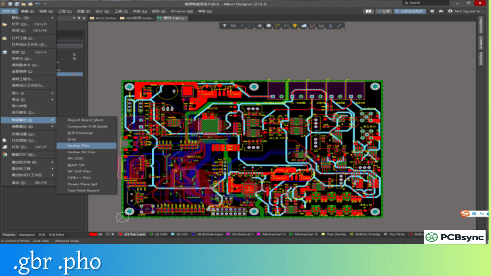
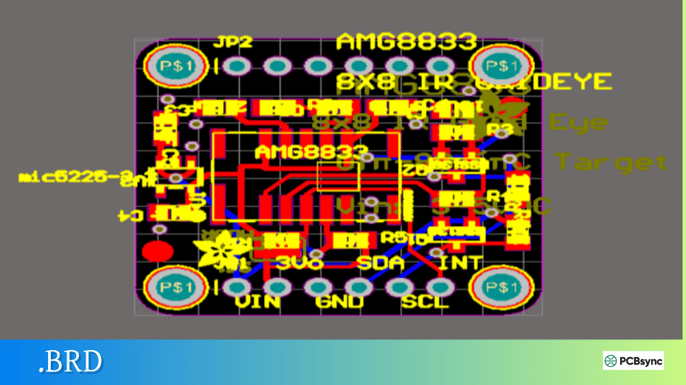
Notes: For PCB fabrication, we require PCB design file in Gerber RS-274X format (most preferred), *.PCB/DDB (Protel, inform your program version) format or *.BRD (Eagle) format. For PCB assembly, we require PCB design file in above mentioned format, drilling file and BOM. Click to download BOM template To avoid file missing, please include all files into one folder and compress it into .zip or .rar format.
What is a Netlist? PCB Connectivity Data Explained
Every time you create a schematic and transfer it to a PCB layout, something happens behind the scenes that makes the magic work. That something is the netlist—a fundamental piece of data that defines how every component in your circuit connects to every other component. Without it, your PCB design software would have no idea which pads should be routed together.
This guide explains what netlists are, how they work in PCB design, and why understanding them helps you catch errors before they become expensive manufacturing mistakes.
A netlist is a text-based description of the electrical connectivity in an electronic circuit. In its simplest form, it’s a list of components and the nodes (connection points) they share. Strip away all the graphical elements from your schematic—the symbols, the wire routing, the page layouts—and what remains is the netlist: pure connectivity information.
The term “net” refers to a single electrical connection that ties multiple component pins together. A netlist, therefore, is simply a collection of all these nets in your design. If you have a resistor connected between power and a microcontroller input, that connection is a net. The complete list of such connections across your entire circuit forms the netlist.
Think of it this way: your schematic is a map showing how to navigate a city, while the netlist is the list of all street intersections and which roads connect them. Both describe the same thing, but from different perspectives. The schematic is visual and human-readable; the netlist is textual and machine-readable.
Why Netlists Matter
Netlists serve as the bridge between schematic capture and PCB layout. When you import your schematic into a layout tool, it’s the netlist data that creates those thin grey “ratsnest” lines showing which pads need connecting. Your routing job is essentially turning that netlist into physical copper traces.
But netlists do more than just transfer data between design stages. They enable:
Design verification before manufacturing
SPICE simulation of circuit behavior
Comparison between design intent and fabrication files
Automated electrical testing of finished boards
Anatomy of a Netlist File
A netlist contains structured data that any compliant software can parse. While formats vary, the core information remains consistent.
Essential Netlist Components
Element
Description
Example
Net Name
Unique identifier for each connection
VCC, GND, SDA, NET001
Reference Designator
Component identifier
U1, R5, C12
Pin Number
Specific pin on component
1, 2, A1, VDD
Component Value
Part specification
10K, 100nF, ATmega328
A typical netlist entry might read: “Net GND connects U1-pin8, C1-pin2, R3-pin1, J1-pin3.” This tells the layout software that all these pins must end up electrically connected on the finished board.
Sample Netlist Structure
Here’s what a simplified netlist looks like in practice:
Each block defines a net name followed by the component pins belonging to that net. This structure tells any compatible layout software exactly how to connect components without ambiguity.
Common Netlist Formats
Unlike Gerber files that follow a universal standard, netlist formats vary across vendors and applications. Understanding the main formats helps when exchanging data between tools.
Netlist Format Comparison
Format
Primary Use
Key Features
SPICE
Circuit simulation
Describes electrical behavior, supports models
EDIF
Data interchange
Vendor-neutral, supports schematics and netlists
IPC-D-356
Manufacturing/test
Standard for bare board testing
Verilog/VHDL
FPGA development
Hardware description language
OrCAD
Cadence tools
Native format for OrCAD/Allegro
Altium
Altium Designer
Proprietary format, auto-synchronized
For PCB manufacturing, the IPC-D-356 format deserves special attention. This ASCII text file format, standardized by IPC (Association Connecting Electronics Industries), includes net names, pin locations, and XY coordinates. Fabricators use it to verify that Gerber files match design intent before production.
SPICE Netlists for Simulation
SPICE netlists describe not just connectivity but also component electrical behavior. They’re used for analog and mixed-signal simulation before committing to a physical design. A SPICE netlist includes:
Component instance names and values
Node connections between components
Subcircuit definitions for complex parts
Simulation commands and analysis types
Engineers use SPICE netlists to verify that circuits work as intended—checking gain, frequency response, stability, and other electrical characteristics—before spending money on prototypes.
How Netlists Flow Through PCB Design
Understanding the netlist workflow helps prevent connectivity errors that can kill a project.
From Schematic to Layout
The journey starts when you create or compile your schematic. Your CAD software generates a netlist from the schematic drawings, extracting connectivity from the wire segments and component symbols. This netlist then drives the PCB layout process.
Design Stage
Netlist Role
Schematic Capture
Generated from wire connections
Design Sync
Transfers connectivity to layout
PCB Layout
Creates ratsnest, guides routing
DRC/ERC
Validates connections match rules
Manufacturing
Verifies Gerbers match design intent
Testing
Guides flying probe or fixture test
Modern integrated tools like Altium Designer handle this synchronization automatically—change the schematic, and the PCB netlist updates accordingly. Older or less integrated workflows require manual netlist export and import, creating opportunities for version mismatch errors.
Netlist Verification in Manufacturing
Here’s where netlists become critical for catching errors. When you send Gerber files to a fabricator, those files are graphical—they show copper patterns but don’t explicitly define electrical connections. Errors in Gerber generation or layer assignment can create shorts or opens that aren’t obvious from visual inspection.
By supplying an IPC-D-356 netlist with your fabrication package, you enable a powerful verification step. The manufacturer’s CAM software extracts a reference netlist from your Gerber data, then compares it against your supplied netlist. Any discrepancies—unexpected shorts, missing connections, or mismatched nets—get flagged before production begins.
This comparison catches problems that would otherwise survive until electrical testing:
Incorrect layer polarity assignments
Corrupted Gerber features
Missing or extra drill hits
Operator setup errors in CAM
Creating and Exporting Netlists
Every major PCB design package includes netlist generation capabilities. The process varies by tool, but the fundamentals remain similar.
Netlist Export by Software
Software
Export Method
Common Formats
Altium Designer
File → Fabrication Outputs → Testpoint Report
IPC-D-356A
KiCad
Tools → Generate Netlist
Multiple formats
OrCAD Capture
Tools → Create Netlist
EDIF, Allegro native
Eagle
File → Export → Netlist
Eagle format, SPICE
Cadence Allegro
Netlist → Create Netlist
Native, IPC-D-356
For manufacturing purposes, always export an IPC-D-356A format netlist alongside your Gerber files. This industry-standard format provides the information fabricators need for pre-production verification and bare board electrical testing.
Best Practices for Netlist Management
Following these guidelines prevents connectivity headaches:
Generate from final design: Always create your netlist from the same design revision used to generate Gerbers. A netlist from an earlier revision won’t match your fabrication files.
Verify before export: Run design rule checks (DRC) and electrical rule checks (ERC) before generating netlists. These catch obvious connectivity problems at the source.
Include with fab package: Send your IPC-D-356 netlist with every PCB order. The small effort pays off in error prevention.
Document intentional anomalies: If your design includes deliberate shorts (like thermal relief modifications) or other unusual connectivity, note these in your fab documentation to prevent false error reports.
Netlist Errors and Troubleshooting
When things go wrong with connectivity, the netlist is often where you’ll find the evidence—or the cause.
Common Netlist Problems
Issue
Symptom
Typical Cause
Missing net
Pad has no ratsnest connection
Unconnected schematic pin
Extra net
Unexpected connection appears
Accidental wire crossing
Wrong pin
Connection to incorrect component pin
Symbol pin mapping error
Name mismatch
Nets don’t connect across sheets
Inconsistent net naming
Duplicate designator
Same reference used twice
Copy/paste error
Hierarchical designs introduce additional complexity. Nets must correctly pass between schematic sheets through ports or hierarchical pins. A naming inconsistency at any level breaks the connection across the entire hierarchy.
Debugging Netlist Issues
When netlist comparison reports discrepancies, investigate systematically:
Check if the error is in the schematic or layout
Verify net names match across hierarchical boundaries
Confirm footprint pin mappings match schematic symbols
Look for unintentional connections from overlapping wires
Validate that all design files come from the same revision
Your CAD software’s cross-probing features help here—clicking a net in the netlist highlights it in both schematic and layout, making mismatches visible.
What is the difference between a netlist and a schematic?
A schematic is a graphical representation of a circuit showing component symbols and wire connections in a visual format humans can easily read and understand. A netlist is a text-based extraction of only the connectivity information from that schematic—it lists which pins connect to which other pins without any visual representation. Both describe the same electrical connections, but in different formats optimized for different purposes.
Why should I send a netlist with my Gerber files?
Sending an IPC-D-356 netlist with your fabrication files enables pre-production verification that can catch errors before manufacturing begins. The fabricator’s CAM software compares your netlist against the connectivity inferred from your Gerber data. Any discrepancies—shorts, opens, or missing connections—get identified and reported before cutting any copper, potentially saving significant time and cost.
Can I create a schematic from a netlist?
Technically, yes—a netlist contains all the connectivity information needed to reconstruct a circuit. However, the result would be functionally correct but graphically meaningless: components scattered randomly with wires connecting appropriate pins. The logical organization, grouping, and readability of a human-designed schematic cannot be recovered from a netlist alone. Some tools offer “netlist to schematic” features, but the output requires significant manual cleanup.
What netlist format should I use for simulation?
For circuit simulation, use SPICE format netlists. SPICE netlists include not only connectivity but also component electrical models and simulation parameters. Your simulator—whether LTspice, PSpice, ngspice, or others—requires this format to perform transient, AC, DC, or other analyses. Most schematic capture tools can export SPICE netlists directly or through add-on utilities.
How do I fix netlist synchronization errors?
Netlist synchronization errors occur when schematic and layout connectivity diverge. To fix them, first identify whether the schematic or layout is correct. Then use your CAD tool’s synchronization features—Update PCB, Import Changes, or similar commands—to push corrections from the authoritative source to the other document. Always run DRC/ERC checks afterward to confirm the fix didn’t introduce new problems.
Conclusion
The netlist may not be glamorous, but it’s fundamental to everything that happens after schematic capture. This simple text-based connectivity description enables schematic-to-layout transfer, powers simulation, enables manufacturing verification, and guides electrical testing of finished boards.
Understanding netlists helps you work more effectively with your design tools, troubleshoot connectivity problems faster, and catch errors before they reach production. Take time to include IPC-D-356 netlists in your fabrication packages—the verification capability they provide is well worth the minimal extra effort.
Whether you’re synchronizing schematics with layouts, setting up SPICE simulations, or sending files to manufacturing, the netlist remains the authoritative record of what connects to what. Master this foundational concept, and you’ll navigate PCB design with greater confidence and fewer costly surprises.
Inquire: Call 0086-755-23203480, or reach out via the form below/your sales contact to discuss our design, manufacturing, and assembly capabilities.
Quote: Email your PCB files to Sales@pcbsync.com (Preferred for large files) or submit online. We will contact you promptly. Please ensure your email is correct.
Notes: For PCB fabrication, we require PCB design file in Gerber RS-274X format (most preferred), *.PCB/DDB (Protel, inform your program version) format or *.BRD (Eagle) format. For PCB assembly, we require PCB design file in above mentioned format, drilling file and BOM. Click to download BOM template To avoid file missing, please include all files into one folder and compress it into .zip or .rar format.


