Inquire: Call 0086-755-23203480, or reach out via the form below/your sales contact to discuss our design, manufacturing, and assembly capabilities.
Quote: Email your PCB files to Sales@pcbsync.com (Preferred for large files) or submit online. We will contact you promptly. Please ensure your email is correct.
Notes: For PCB fabrication, we require PCB design file in Gerber RS-274X format (most preferred), *.PCB/DDB (Protel, inform your program version) format or *.BRD (Eagle) format. For PCB assembly, we require PCB design file in above mentioned format, drilling file and BOM. Click to download BOM template To avoid file missing, please include all files into one folder and compress it into .zip or .rar format.
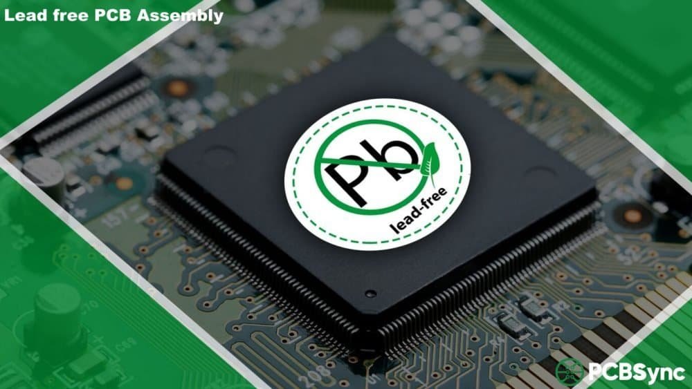
The electronics manufacturing landscape changed dramatically when the European Union introduced RoHS regulations in 2006. As someone who’s worked through this transition in PCB assembly, I’ve seen firsthand how lead-free processes transformed our industry. Today, understanding lead-free PCB assembly isn’t just about compliance—it’s about delivering reliable products that meet global environmental standards while maintaining the quality our customers expect.
Lead-free PCB assembly represents a fundamental shift from traditional tin-lead soldering processes to alternative alloy compositions that eliminate or drastically reduce lead content. This manufacturing approach involves using solder alloys, surface finishes, and components that comply with environmental regulations, particularly the RoHS directive which restricts lead content to below 1,000 parts per million (0.1%) in homogeneous materials.
The transition wasn’t simply about swapping out solder paste. It required a complete reevaluation of materials, equipment capabilities, process parameters, and quality standards. Every aspect of the assembly line needed adjustment—from the reflow oven temperature profiles to the cleaning agents used post-assembly.
Why the Industry Moved to Lead-Free Assembly
Lead contamination in soil and water systems from improperly disposed electronics became a serious environmental concern by the early 2000s. Lead is a known neurotoxin that causes developmental problems in children and various health issues in adults. When millions of electronic devices ended up in landfills annually, the toxic load entering ecosystems became unsustainable.
Beyond environmental concerns, there are compelling business reasons for lead-free assembly. Access to European, Chinese, and California markets now requires RoHS compliance. Companies that failed to transition found themselves locked out of major markets. Additionally, many large OEMs now mandate lead-free assembly even for products not bound by regulatory requirements, making it a competitive necessity rather than just a legal one.
Understanding RoHS Compliance for PCB Assembly
The Restriction of Hazardous Substances (RoHS) directive originated in the EU as Directive 2002/95/EC. What started as RoHS 1 in 2006 has evolved through RoHS 2 (2011) and RoHS 3 (2015), with each iteration expanding scope and adding restricted substances. Currently, RoHS restricts ten categories of hazardous substances in electrical and electronic equipment.
The Ten RoHS Restricted Substances
Substance
Maximum Concentration
Primary Concern
Lead (Pb)
0.1% (1000 ppm)
Neurotoxin, environmental contamination
Mercury (Hg)
0.1% (1000 ppm)
Severe toxicity to nervous system
Cadmium (Cd)
0.01% (100 ppm)
Carcinogenic, kidney damage
Hexavalent Chromium (Cr VI)
0.1% (1000 ppm)
Carcinogenic, respiratory damage
Polybrominated Biphenyls (PBB)
0.1% (1000 ppm)
Flame retardant, endocrine disruptor
Polybrominated Diphenyl Ethers (PBDE)
0.1% (1000 ppm)
Flame retardant, developmental toxicity
Bis(2-Ethylhexyl) phthalate (DEHP)
0.1% (1000 ppm)
Plasticizer, reproductive toxicity
Benzyl butyl phthalate (BBP)
0.1% (1000 ppm)
Plasticizer, endocrine disruptor
Dibutyl phthalate (DBP)
0.1% (1000 ppm)
Plasticizer, reproductive toxicity
Diisobutyl phthalate (DIBP)
0.1% (1000 ppm)
Plasticizer, reproductive toxicity
These concentration limits apply to each homogeneous material in the product. A homogeneous material is defined as a material of uniform composition throughout that cannot be mechanically separated into different materials. This means you can’t dilute a high-concentration substance by mixing it with compliant materials—each distinct material layer must meet the thresholds independently.
RoHS Compliance Scope and Application
RoHS applies to manufacturers, importers, and distributors selling electrical and electronic equipment in the EU market, regardless of where the products are manufactured. This global reach means a PCB assembled in Asia for a product sold in Europe must be RoHS compliant. Many countries beyond the EU have adopted similar regulations, including China’s RoHS, South Korea’s regulations, and California’s RoHS law.
For PCB assemblers, compliance involves the entire supply chain. You must verify that bare boards, components, solder materials, fluxes, cleaning agents, and even the packaging materials meet RoHS requirements. Documentation and traceability become critical—you need certificates of compliance from suppliers and must maintain records proving your assembly process doesn’t introduce restricted substances.
Lead-Free Solder Alloys: The Core of the Transition
The most visible change in lead-free PCB assembly is the solder alloy itself. Traditional eutectic tin-lead solder (63% tin, 37% lead) had an ideal melting point of 183°C and excellent wetting properties. Finding lead-free alternatives that could match this performance took years of materials research.
SAC Alloys: The Industry Standard
Tin-silver-copper (SAC) alloys emerged as the primary replacement for tin-lead solder. The most widely adopted formulation is SAC305, which contains:
96.5% Tin (Sn)
3.0% Silver (Ag)
0.5% Copper (Cu)
SAC305 offers several advantages that made it the industry standard. It’s near-eutectic with a narrow melting range (217-220°C), provides good mechanical strength, and demonstrates reliable thermal fatigue performance. The alloy wets adequately to copper and common surface finishes, though not quite as readily as tin-lead.
The higher melting point compared to tin-lead (about 34°C higher) is both the biggest challenge and a key reliability factor. While it requires higher reflow temperatures and puts more thermal stress on components and boards, the resulting solder joints can withstand higher operating temperatures without degradation.
Alternative Lead-Free Alloys
Alloy Type
Composition
Melting Point
Applications
SAC305
Sn96.5/Ag3.0/Cu0.5
217-220°C
General SMT assembly
SAC105
Sn98.5/Ag1.0/Cu0.5
217-220°C
Cost-sensitive, wave soldering
SAC0307
Sn99/Ag0.3/Cu0.7
227-228°C
Lower silver content, cost reduction
Sn-Cu
Sn99.3/Cu0.7
227°C
Wave soldering, no silver
SN100C
Sn/Cu/Ni/Ge
227°C
Wave soldering alternative
Choosing the right alloy depends on your assembly method, cost constraints, and reliability requirements. Wave soldering operations often prefer lower silver content alloys or tin-copper formulations to manage costs, since wave soldering consumes more solder than reflow processes. For high-reliability applications like aerospace or medical devices, SAC305 remains the preferred choice despite higher material costs.
Critical Process Differences in Lead-Free Assembly
Moving to lead-free assembly isn’t as simple as changing the solder paste. The higher melting temperatures and different alloy characteristics affect every stage of the assembly process.
Temperature Profile Challenges
Lead-free reflow requires peak temperatures typically between 240-260°C, compared to 210-220°C for tin-lead. This 30-40°C increase creates several challenges:
Board Material Stress: Standard FR4 laminates must have higher glass transition temperatures (Tg) to withstand lead-free processing. Many legacy designs used 140°C Tg materials, but lead-free assembly typically requires 170°C or higher Tg laminates. For multilayer boards with six or more layers, 180°C Tg materials provide better reliability.
The coefficient of thermal expansion (CTE) mismatch between board and components becomes more pronounced at higher temperatures. This can cause pad cratering, barrel cracking in plated through-holes, or delamination in poorly specified board materials.
Component Tolerance: Not all components can survive the higher temperatures. Older electrolytic capacitors, some connectors, and certain plastic components have maximum temperature ratings below lead-free processing temperatures. Component manufacturers have largely addressed this by releasing 260°C-capable versions, but legacy designs may require component substitutions.
Moisture Sensitivity: The higher temperatures make moisture-sensitive devices (MSDs) much more vulnerable. Moisture trapped in plastic component packages can rapidly expand at 260°C, causing “popcorning” failures. This makes moisture management more critical—components must be properly baked before assembly and exposure time to ambient humidity must be carefully controlled.
Reflow Profile Development
A proper lead-free reflow profile typically includes four zones:
Preheat (150-180°C): Gradually raises board temperature to activate flux and minimize thermal shock
Soak (180-200°C): Holds temperature long enough for uniform heating across the board
Reflow (217-260°C): Raises temperature above the solder’s liquidus point for 30-90 seconds
Cooling: Controlled cooling to prevent thermal shock and ensure proper metallurgical grain structure
The time above liquidus (TAL) is particularly critical. Too short and you get incomplete wetting and weak joints. Too long and you can damage components or cause excessive copper dissolution from pads. Most processes target 30-90 seconds TAL depending on board complexity.
Wave Soldering Modifications
For through-hole assembly, lead-free wave soldering requires significant equipment modifications. Pot temperatures typically run at 260-275°C, compared to 250°C for tin-lead. This higher temperature accelerates copper leaching from boards and pads, requiring more frequent bath maintenance and composition monitoring.
The solder pot itself needs upgrades. Tin-rich lead-free alloys are more aggressive toward mild steel pots, potentially requiring titanium or coated pots for longevity. Additionally, nitrogen blanketing becomes more important to minimize dross formation and ensure consistent wetting.
Lead-Free Surface Finishes
The bare PCB’s surface finish must also be lead-free compliant. This eliminates traditional HASL (Hot Air Solder Leveling) which uses tin-lead solder. Several lead-free alternatives have become standard:
In my experience, ENIG has become the most popular choice for lead-free assembly. The flat, uniform surface enables fine-pitch component placement, and the gold layer provides excellent corrosion protection during storage. However, it’s more expensive than HASL and requires careful process control to avoid nickel corrosion issues.
OSP offers the flattest surface and works well for immediate assembly, but its limited shelf life makes it problematic for inventory-based operations. Boards must be assembled within 30 days or the OSP layer oxidizes, requiring reapplication.
Quality Standards for Lead-Free Assembly
Lead-free assembly brought new quality challenges that required updates to industry standards. The IPC (Association Connecting Electronics Industries) developed comprehensive guidelines to address these changes.
IPC J-STD-001: Requirements for Soldered Assemblies
IPC J-STD-001 is the definitive standard for soldering processes and materials. The current revision (J-STD-001J as of 2024) provides detailed requirements for both leaded and lead-free assembly. The standard covers:
Solder alloy specifications and purity requirements
Flux activity levels and residue acceptability
Temperature profile requirements for reflow and wave soldering
Visual acceptance criteria for solder joints
Component handling and ESD protection
Cleaning and residue requirements
The standard classifies products into three classes based on end-use requirements:
Class 1: General consumer electronics where cosmetic appearance and long-term reliability are less critical Class 2: Dedicated service electronics where continued performance is required Class 3: High-reliability electronics where failure could be life-threatening
Each class has progressively stricter requirements for process control and joint acceptance. Medical devices and aerospace electronics typically fall under Class 3, requiring the most rigorous controls and documentation.
IPC-A-610: Acceptability of Electronic Assemblies
While J-STD-001 defines the process, IPC-A-610 provides visual acceptance criteria for finished assemblies. This standard includes hundreds of high-resolution photographs showing what constitutes an acceptable solder joint versus a defect.
For lead-free assembly, A-610 addresses specific issues like:
Different wetting appearance of SAC alloys (often grainier than tin-lead)
Acceptable fillet heights and shapes for lead-free solder
Component standoff requirements at higher processing temperatures
Visual differences in flux residues from lead-free fluxes
The standard is invaluable for training inspectors and establishing consistent quality criteria across different facilities and contract manufacturers.
Demonstrating RoHS compliance requires rigorous testing and documentation. Simply using lead-free materials isn’t sufficient—you must be able to prove compliance through analytical testing.
RoHS Testing Methods
Accredited testing laboratories use several techniques to verify substance concentrations:
X-Ray Fluorescence (XRF): Non-destructive screening method that can detect most RoHS substances. Fast and economical for initial screening, but cannot detect phthalates and has limited accuracy for complex matrices.
ICP-AES (Inductively Coupled Plasma Atomic Emission Spectroscopy): Destructive test that provides highly accurate concentration measurements for heavy metals. Samples are dissolved in acid and analyzed, making it the definitive method for metals testing.
GC-MS (Gas Chromatography-Mass Spectrometry): Required for detecting brominated flame retardants and phthalates. More expensive than XRF or ICP, but essential for complete RoHS compliance verification.
Most manufacturers use a tiered approach: XRF screening for incoming materials, with full ICP and GC-MS testing performed on production samples periodically or when new suppliers or materials are introduced.
RoHS Declarations of Compliance from all suppliers
Material composition analysis reports
Process validation documentation
Component traceability through lot codes
Assembly traveler records showing materials used
Periodic re-testing results
This documentation must be maintained for regulatory audits and provided to customers upon request. Many contract manufacturers now use materials management systems that track RoHS status throughout the production process, flagging any non-compliant materials before they reach the assembly line.
Component Selection and Supply Chain Management
One of the biggest challenges in transitioning to lead-free assembly was ensuring component availability. Early in the transition, not all components were available in lead-free terminations, requiring extensive redesigns or finding alternate parts.
Lead-Free Component Considerations
Components for lead-free assembly must meet several requirements:
Termination Finish: Component leads or terminations must be lead-free compatible. Common terminations include pure tin, tin-silver, or tin-copper platings. Pure tin terminations require careful attention to tin whisker growth prevention.
Temperature Rating: Components must be rated for the higher temperatures of lead-free processing, typically 260°C peak temperature tolerance. This is marked as “Pb-Free” or “RoHS Compliant” in datasheets.
Moisture Sensitivity Level: With higher processing temperatures, moisture sensitivity becomes more critical. Many components moved to lower MSL ratings or require more careful handling and baking procedures.
Supply Chain Verification
Managing a lead-free supply chain requires robust processes:
Supplier Qualification: Verify suppliers can provide RoHS-compliant materials with proper documentation
Approved Vendor Lists: Maintain lists of qualified suppliers with current compliance status
Incoming Inspection: Verify incoming materials match RoHS declarations, spot-checking with XRF testing
Segregation: Keep lead-free and leaded materials completely separate to prevent contamination
Training: Ensure procurement and receiving staff understand RoHS requirements and verification procedures
Cross-contamination is a serious concern. Even trace lead contamination in a lead-free assembly can cause compliance failures. I’ve seen manufacturers implement color-coded storage systems, dedicated tools for lead-free materials, and separate assembly lines to maintain segregation.
Common Challenges and Solutions
After years of working with lead-free assembly, certain challenges appear consistently. Understanding these issues and their solutions can save significant time and frustration.
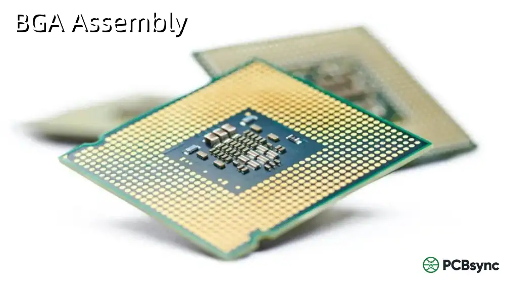
Challenge: Excessive Voiding in BGA Joints
Lead-free solder paste tends to produce more voids in solder joints, particularly in ball grid array (BGA) components. Voids above 25% of joint area can compromise reliability.
Solutions:
Use vacuum reflow for critical BGAs
Optimize reflow profile to allow more outgassing time in the soak zone
Select solder pastes with enhanced wetting agents
Ensure proper stencil design with adequate paste release
Challenge: Copper Dissolution in Wave Soldering
The higher pot temperatures in lead-free wave soldering cause faster copper dissolution from pads and holes, altering solder bath composition.
Solutions:
Monitor copper content regularly and maintain between 0.5-0.9%
Use copper-containing alloys (like SAC305) to stabilize copper levels
Implement proper wave contact time—not too long
Use nitrogen blanketing to reduce oxidation and dross
Challenge: Tin Whisker Growth
Pure tin terminations on components can grow conductive “whiskers” over time, potentially causing short circuits in high-density assemblies.
Solutions:
Specify components with tin-alloy terminations (tin-silver or tin-copper preferred)
Apply conformal coatings to suppress whisker growth
Design with adequate spacing for whisker-prone components
Avoid pure tin finishes on high-voltage or high-reliability products
Useful Resources for Lead-Free PCB Assembly
Staying current with lead-free assembly best practices requires access to reliable resources. Here are the most valuable references I’ve found:
Standards and Guidelines
IPC J-STD-001 (Latest Revision J): Available from IPC Store
IPC-A-610 (Acceptability of Electronic Assemblies): Companion to J-STD-001
IPC-7711/7721: Rework and repair guidelines for lead-free assemblies
IPC-1752: Materials declaration standard for substance content
iNEMI Lead-Free Solder Project: Comprehensive research on lead-free materials and processes
NIST Lead-Free Solder Database: Material properties and reliability data
SMTA (Surface Mount Technology Association): Technical papers and webinars on lead-free assembly
Training and Certification
IPC Certification Programs: Hands-on training for J-STD-001 and A-610
SMTA Courses: Specialized training on lead-free processes
Component manufacturer resources: Many suppliers offer lead-free transition guides
Looking Forward: The Future of Lead-Free Assembly
The electronics industry continues to evolve beyond basic lead-free compliance. Several trends are shaping the future:
Lower Temperature Solders: Research into bismuth-containing and other low-melting-point alloys aims to reduce process temperatures while maintaining reliability. This could enable use of more temperature-sensitive components and reduce energy consumption.
Sintering Technologies: Silver sintering and other pressure-assisted joining technologies may eventually supplement or replace some soldering applications, particularly for high-temperature electronics like power modules.
Expanded Substance Restrictions: Future regulations may restrict additional substances, requiring continued materials innovation. PFAS (per- and polyfluoroalkyl substances) are already under regulatory scrutiny in Europe.
Circular Economy Considerations: Beyond restricting hazardous substances, future regulations will likely emphasize recyclability and circular economy principles, influencing material selection and assembly design.
The lead-free transition taught us that major manufacturing changes are possible when driven by clear regulatory requirements and supported by industry collaboration. Whatever challenges lie ahead, the foundation built during the lead-free transition provides a proven framework for adaptation.
Frequently Asked Questions
Q: Can lead-free and leaded assemblies be run on the same production line?
A: It’s technically possible but not recommended. Cross-contamination is a serious risk—even trace lead in a lead-free assembly can cause compliance failures. If you must share equipment, implement rigorous cleaning procedures between runs, use dedicated tooling, and thoroughly document your segregation processes. Most manufacturers find it more reliable to maintain separate dedicated lines.
Q: How does lead-free solder joint reliability compare to tin-lead?
A: Modern lead-free solder joints can match or exceed tin-lead reliability when properly processed. SAC alloys show better high-temperature performance and creep resistance than tin-lead. However, they’re more brittle and less tolerant of drop-shock impacts, making them less ideal for handheld devices. Thermal cycling reliability is comparable when proper alloys and processes are used. The key is optimizing your specific process—simply swapping materials without process development rarely produces equivalent results.
Q: What’s the typical cost increase for lead-free assembly?
A: Material costs typically increase 10-20% due to higher silver content in SAC alloys and more expensive surface finishes. Process costs may increase 5-15% from higher energy consumption (higher reflow temperatures), more frequent equipment maintenance, and additional quality controls. However, these costs have decreased significantly since the early transition as processes matured and economies of scale improved. For many manufacturers, lead-free is now the baseline cost rather than a premium option.
Q: Are there exemptions to RoHS requirements?
A: Yes, RoHS includes specific exemptions where lead-free alternatives aren’t technically feasible. These include high-lead solders (over 85% lead), certain specialty glasses and ceramics, and specific component applications. Medical devices and industrial monitoring equipment have extended compliance timelines. However, exemptions are regularly reviewed and may be phased out as alternatives become available. Relying on exemptions for long-term products is risky.
Q: How often should I revalidate my lead-free assembly process?
A: Formal process revalidation should occur whenever you change materials (different solder paste batch, new component suppliers), equipment (new reflow oven, different settings), or board designs (new materials, different thermal mass). Additionally, periodic revalidation every 12-24 months helps catch process drift. Continuous monitoring through SPC (Statistical Process Control) lets you detect issues before they become failures. High-reliability operations often perform mini-revalidations quarterly to ensure process consistency.
Inquire: Call 0086-755-23203480, or reach out via the form below/your sales contact to discuss our design, manufacturing, and assembly capabilities.
Quote: Email your PCB files to Sales@pcbsync.com (Preferred for large files) or submit online. We will contact you promptly. Please ensure your email is correct.
Notes: For PCB fabrication, we require PCB design file in Gerber RS-274X format (most preferred), *.PCB/DDB (Protel, inform your program version) format or *.BRD (Eagle) format. For PCB assembly, we require PCB design file in above mentioned format, drilling file and BOM. Click to download BOM template To avoid file missing, please include all files into one folder and compress it into .zip or .rar format.


