Inquire: Call 0086-755-23203480, or reach out via the form below/your sales contact to discuss our design, manufacturing, and assembly capabilities.
Quote: Email your PCB files to Sales@pcbsync.com (Preferred for large files) or submit online. We will contact you promptly. Please ensure your email is correct.
Notes: For PCB fabrication, we require PCB design file in Gerber RS-274X format (most preferred), *.PCB/DDB (Protel, inform your program version) format or *.BRD (Eagle) format. For PCB assembly, we require PCB design file in above mentioned format, drilling file and BOM. Click to download BOM template To avoid file missing, please include all files into one folder and compress it into .zip or .rar format.
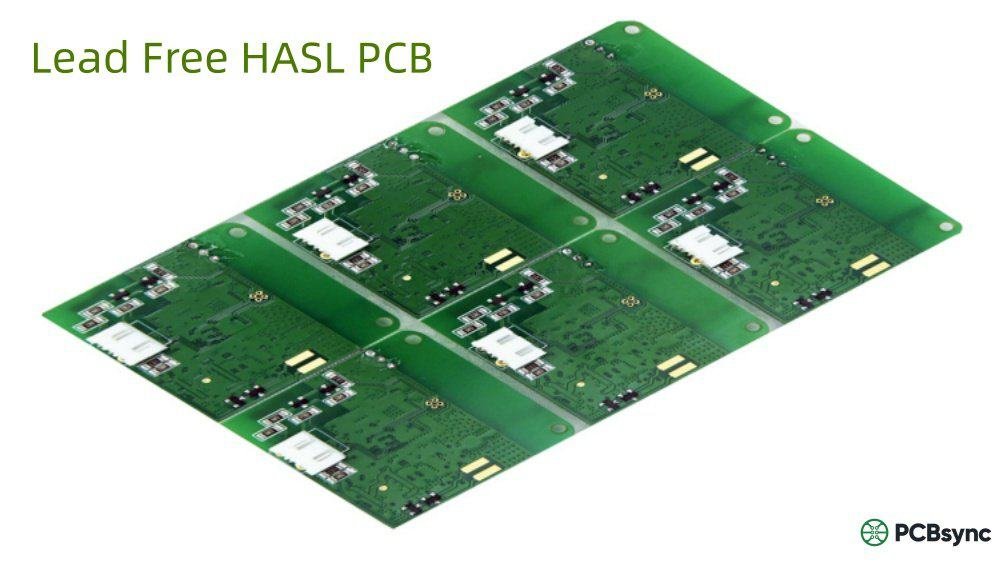
If you’ve been working with PCBs for any length of time, you’ve probably encountered the term HASL more times than you can count. Hot Air Solder Leveling has been the workhorse of PCB surface finishes for decades, and for good reason—it works, it’s reliable, and it won’t break your budget.
But here’s the thing: the industry has changed. RoHS compliance isn’t optional anymore if you’re selling into Europe or working with environmentally conscious clients. That’s where lead-free HASL comes in. It gives you the same reliable performance you’ve come to expect from traditional HASL, minus the environmental baggage.
Having worked on countless PCB projects over the years, I’ve seen engineers overthink surface finish selection—and I’ve also seen projects fail because of underthinking it. The key is understanding what each finish does well and where its limitations lie. HASL isn’t the right answer for every application, but for the right applications, it’s hard to beat.
In this guide, I’ll walk you through everything you need to know about HASL PCB finishes—from the nitty-gritty of the process to the practical trade-offs you’ll face when choosing between HASL and alternatives like ENIG or OSP. Whether you’re designing a prototype or scaling up for production, this article will help you make an informed decision.
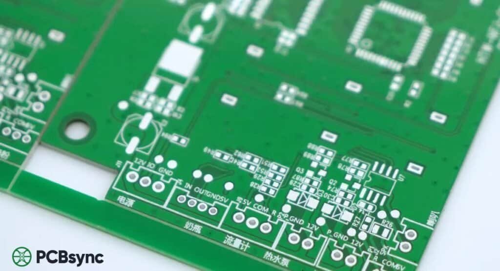
HASL stands for Hot Air Solder Leveling. It’s a surface finish process where exposed copper pads on a PCB are coated with molten solder, then leveled using high-pressure hot air knives. The result is a protective layer that prevents oxidation and provides an excellent solderable surface for component assembly.
The traditional HASL process uses a eutectic tin-lead alloy (63% tin, 37% lead) with a melting point of 183°C. This composition has been the industry standard for decades because it offers excellent wetting characteristics, low cost, and proven reliability.
However, since the EU’s Restriction of Hazardous Substances (RoHS) directive came into effect in 2006, manufacturers have increasingly shifted to lead-free alternatives. Lead-free HASL uses tin-based alloys—typically tin-copper (SnCu) or tin-silver-copper (SAC)—to achieve RoHS compliance while maintaining the core benefits of the HASL process.
Why Lead-Free HASL Matters
RoHS Compliance and Environmental Regulations
The RoHS directive restricts lead content to less than 0.1% (1000 ppm) by weight in electronic equipment. Traditional tin-lead HASL contains 37% lead, which is far above this threshold. If your product is destined for the EU market—or increasingly, markets in China, South Korea, Japan, and California—lead-free HASL is not optional; it’s mandatory.
Beyond regulatory compliance, there’s a practical consideration: supply chain simplification. Many component manufacturers now only offer lead-free parts. Using lead-free HASL ensures compatibility throughout your assembly process without the need for separate production lines.
Health and Environmental Benefits
Lead is a neurotoxin that accumulates in the body and can cause severe health problems with prolonged exposure. For manufacturing workers handling PCBs daily, this is a real occupational hazard. Lead-free HASL eliminates this risk at the source.
From an environmental perspective, electronic waste is a growing concern. PCBs containing lead pose a long-term contamination risk when they end up in landfills. The lead can leach into groundwater, affecting ecosystems and potentially entering the food chain.
Lead-Free HASL Alloy Compositions
Not all lead-free HASL finishes are created equal. The alloy composition directly affects melting point, wetting characteristics, mechanical strength, and cost. Here are the most common options:
Alloy Type
Composition
Melting Point
Key Characteristics
Sn-Cu (SN100C)
99.3% Sn, 0.6% Cu, 0.05% Ni + Ge
227°C
Most common, cost-effective, good wetting
SAC305
96.5% Sn, 3.0% Ag, 0.5% Cu
217-220°C
Higher strength, better fatigue resistance, more expensive
Sn-Bi
~95% Sn, ~5% Bi
138-170°C
Lower temp, brittle, limited use
Traditional SnPb
63% Sn, 37% Pb
183°C
Not RoHS compliant, bright finish
The Sn-Cu alloy (often marketed as SN100C or similar) is the most widely used for lead-free HASL because it balances cost, availability, and performance. The addition of small amounts of nickel and germanium helps control copper dissolution in the solder pot and prevents surface oxidation.
Understanding the HASL process helps you appreciate why certain design constraints exist and how to work within them. Here’s what happens to your PCB during HASL finishing:
Step 1: Surface Preparation
The PCB undergoes thorough cleaning to remove contaminants, oils, and oxide layers from the copper surfaces. This typically involves a micro-etching process that creates a slightly roughened surface for better solder adhesion. Any contamination at this stage will result in poor wetting and potential solderability issues.
Step 2: Flux Application
A flux layer is applied to the board—either by spray, foam, or immersion. The flux serves multiple purposes: it removes any remaining oxides, improves solder wetting, and prevents re-oxidation during the heating process. The flux chemistry must be compatible with the lead-free solder alloy.
Step 3: Solder Immersion
The board is immersed in a bath of molten lead-free solder, typically maintained at 245-275°C (significantly higher than the 200-210°C used for leaded HASL). The board remains in the solder bath for 2-3 seconds, allowing the solder to coat all exposed copper surfaces including pads and plated-through holes.
Step 4: Hot Air Leveling
As the board exits the solder bath, it passes between hot air knives—high-pressure jets of air heated above the solder’s melting point. These air knives remove excess solder and level the remaining coating. The air knife angle, pressure, and temperature are carefully controlled to achieve consistent coating thickness.
There are two main equipment configurations: vertical (the board is dipped vertically into the solder bath) and horizontal (the board passes horizontally through the process). Horizontal systems generally provide better planarity but are less common.
Step 5: Cooling and Cleaning
The board undergoes controlled cooling to solidify the solder coating without introducing thermal stress. Rapid, uncontrolled cooling can cause micro-cracks in the solder layer. After cooling, the board is cleaned to remove flux residues and inspected for coating quality.
HASL PCB Specifications and Thickness
When specifying HASL finish for your PCBs, here are the key parameters to understand:
Parameter
Lead-Free HASL
Leaded HASL
Typical Thickness
0.5-2.0 mils (12.5-50 μm)
1.0-2.5 mils (25-60 μm)
Process Temperature
245-275°C
200-210°C
Shelf Life
6-12 months
12+ months
Minimum Pitch
≥0.5mm (20 mil)
≥0.5mm (20 mil)
RoHS Compliance
Yes
No
Surface Appearance
Matte, slightly dull
Bright, shiny
Note that lead-free HASL typically produces a thinner coating than leaded HASL. This is partly due to the higher surface tension of lead-free solders, which actually works in your favor for coplanarity on smaller pads.
Advantages of Lead-Free HASL
Lead-free HASL offers several compelling benefits that have kept it relevant despite the emergence of newer surface finish technologies:
Excellent Solderability: The pre-tinned surface provides outstanding wetting characteristics during assembly. Components solder easily, and the finish withstands multiple reflow cycles without significant degradation.
Cost-Effective: HASL remains one of the most economical surface finishes available. The process is well-established with mature equipment and consumables.
RoHS Compliant: Lead-free HASL meets all current environmental regulations, including EU RoHS, China RoHS, and similar directives worldwide.
Long Shelf Life: When properly stored in vacuum-sealed packaging with desiccants, lead-free HASL boards maintain solderability for 6-12 months—adequate for most production schedules.
Reworkability: Unlike some finishes, HASL-coated boards can be reworked relatively easily. Damaged areas can be resoldered without extensive preparation.
Built-in Quality Check: The HASL process exposes boards to temperatures up to 265°C, which can reveal delamination or other substrate defects before expensive components are attached.
Widespread Availability: Virtually every PCB fabricator offers HASL finishing, making it easy to source from multiple suppliers.
Disadvantages and Limitations
No surface finish is perfect, and HASL has some well-known limitations that you need to consider:
Uneven Surface: The hot air leveling process can leave a slightly uneven surface, with solder tending to be thicker on smaller pads due to surface tension effects. This makes HASL unsuitable for fine-pitch components (<0.5mm pitch) and BGA packages.
Thermal Stress: The high process temperatures (up to 275°C for lead-free) can stress the PCB substrate. This limits HASL’s use on thin boards (<0.5mm) and boards with high aspect ratio holes.
Not Suitable for HDI: High-density interconnect designs with micro-vias and fine features generally cannot use HASL due to planarity requirements.
Reduced PTH Diameter: Solder buildup in plated-through holes can reduce the effective hole diameter, potentially causing issues with component insertion.
Higher Processing Temperature: Lead-free HASL requires temperatures 35-65°C higher than leaded HASL, which increases energy consumption and may require high-temperature laminate materials.
Copper Dissolution: The molten solder can dissolve copper from the PCB, requiring careful process control and periodic solder bath maintenance.
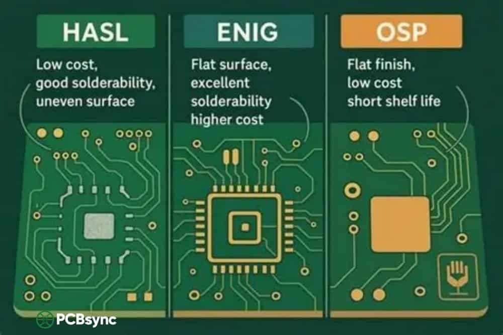
HASL vs. Other Surface Finishes
Choosing the right surface finish involves trade-offs. Here’s how HASL stacks up against the most common alternatives:
Feature
LF-HASL
ENIG
OSP
Imm. Ag
Imm. Sn
Cost
Low
High
Lowest
Medium
Medium
Planarity
Poor
Excellent
Excellent
Excellent
Excellent
Shelf Life
6-12 mo
12+ mo
3-6 mo
6-12 mo
6 mo
Fine Pitch
No
Yes
Yes
Yes
Yes
Reflow Cycles
Multiple
Multiple
1-2
Multiple
Limited
RoHS
Yes
Yes
Yes
Yes
Yes
Key: LF-HASL = Lead-Free HASL, ENIG = Electroless Nickel Immersion Gold, OSP = Organic Solderability Preservative, Imm. Ag = Immersion Silver, Imm. Sn = Immersion Tin
When to Use Lead-Free HASL
Lead-free HASL is an excellent choice for many applications, but it’s not universal. Here’s when it makes sense:
Ideal Applications
Through-hole assemblies: HASL excels when you’re working with through-hole components. The pre-tinned holes solder easily.
Larger SMT components: Components with 0805 or larger footprints, SOICs, and QFPs with 0.5mm+ pitch work well with HASL.
Prototyping and low-volume production: The low cost makes HASL attractive for prototype runs and small batches.
Consumer electronics: Cost-sensitive products where fine-pitch components aren’t required.
Industrial equipment: Rugged applications where solderability and reworkability are valued.
Military/Aerospace (with exemptions): Some applications use leaded HASL under RoHS exemptions for reliability reasons, but lead-free HASL is increasingly accepted.
When to Choose Alternatives
Fine-pitch components (<0.5mm): Use ENIG, OSP, or immersion silver instead.
BGA packages: ENIG is the standard choice for consistent solder ball formation.
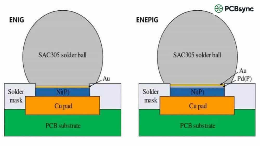
Wire bonding: ENIG or ENEPIG is required for gold or aluminum wire bonding.
Thin boards (<0.5mm): The thermal stress of HASL processing can warp thin substrates.
High-frequency RF: Where impedance control is critical, flatter finishes like ENIG or immersion silver are preferred.
Press-fit connectors: ENIG provides the harder surface needed for press-fit reliability.
Storage and Handling Best Practices
Proper storage is essential to maintain the solderability of HASL-finished boards. Follow these guidelines:
Vacuum seal with desiccant: Store boards in moisture barrier bags with humidity indicator cards and desiccant packets.
Control environment: Maintain storage temperature below 25°C and relative humidity between 30-50%.
Avoid contamination: Handle boards with clean gloves. Skin oils can affect solderability.
First-in, first-out: Use older stock before newer deliveries to prevent exceeding shelf life.
Bake if needed: If boards have absorbed moisture, bake at 125°C for 4 hours before assembly.
Check solderability: For boards stored over 6 months, perform a solderability test per IPC J-STD-003 before production.
Relevant Industry Standards
When specifying HASL finish, reference these standards for quality assurance:
IPC-6012: Qualification and performance specification for rigid PCBs
IPC J-STD-003: Solderability tests for printed boards
IPC-1601: Printed board handling and storage guidelines
IPC J-STD-006: Requirements for electronic grade solder alloys
EU Directive 2011/65/EU (RoHS 3): Restriction of hazardous substances in electronic equipment
Frequently Asked Questions
What is the difference between HASL and lead-free HASL?
Traditional HASL uses a tin-lead (63/37) solder alloy with a melting point of 183°C. Lead-free HASL uses tin-based alloys like Sn-Cu or SAC305, which have higher melting points (217-227°C) but contain no lead. Lead-free HASL is RoHS compliant, while traditional HASL is not. The lead-free version typically produces a slightly thinner, more uniform coating but with a duller appearance.
Can HASL be used for fine-pitch components?
No, HASL is not recommended for components with pitches below 0.5mm (20 mil). The inherent non-planarity of the HASL process makes it unsuitable for fine-pitch QFPs, BGAs, and other high-density packages. For these applications, use ENIG, OSP, or immersion silver, which provide the flat surfaces necessary for accurate component placement and reliable solder joints.
How long does HASL finish last?
Lead-free HASL typically maintains good solderability for 6-12 months when stored properly in vacuum-sealed packaging with desiccant at controlled temperature (<25°C) and humidity (30-50% RH). Leaded HASL can last 12+ months under similar conditions. After this period, solderability testing per IPC J-STD-003 is recommended before assembly.
Is lead-free HASL more expensive than leaded HASL?
Lead-free HASL is marginally more expensive than leaded HASL, typically 5-15% higher. This premium comes from the higher processing temperatures required (more energy consumption), the cost of lead-free solder alloys, and the need for high-temperature laminate materials. However, both are still among the most economical surface finishes available—significantly cheaper than ENIG.
Why does my lead-free HASL board look dull compared to leaded HASL?
This is completely normal. Lead-free solder alloys naturally produce a more matte, slightly grayish appearance compared to the bright, shiny finish of leaded HASL. This visual difference does not indicate a quality issue—the duller appearance has no impact on solderability or performance. It’s simply a characteristic of lead-free alloys.
Useful Resources and Downloads
For further reading and technical specifications, consult these resources:
IPC Standards: www.ipc.org – Purchase IPC-6012, J-STD-003, and related specifications
RoHS Directive: EUR-Lex EU RoHS – Official EU RoHS directive text
Lead-Free Solder Data: iNEMI Lead-Free Resources – Research on lead-free solder alloys and processes
SAC Alloy Data: AIM Solder Comparison PDF – Technical comparison of tin-silver-copper alloy variants
Cost Analysis: HASL vs. Premium Finishes
Understanding the true cost impact of surface finish selection requires looking beyond the per-board price. Here’s a realistic comparison based on typical industry pricing:
For a standard 4-layer board (100mm x 100mm), the surface finish cost difference is approximately: Lead-free HASL serves as the baseline, ENIG adds roughly $0.50-$1.00 per board, OSP reduces cost by $0.10-$0.20 per board, and immersion silver adds about $0.20-$0.40 per board. These numbers scale roughly linearly with board area.
However, the surface finish cost is only part of the equation. You also need to consider assembly yield—a finish that causes more solder defects will increase your rework costs and scrap rate. For most through-hole and large SMT applications, HASL’s excellent solderability means fewer assembly issues and lower total cost of ownership.
For prototype and small-volume production, HASL’s low upfront cost makes it the obvious choice when technically suitable. At higher volumes (10,000+ boards), the economics shift slightly as assembly efficiency becomes more important, but HASL remains competitive for appropriate applications.
Design Considerations for HASL PCBs
When designing a PCB that will use HASL finishing, there are several factors to keep in mind to ensure optimal results:
Pad Size and Geometry
Due to surface tension effects during the HASL process, smaller pads tend to accumulate more solder than larger pads. This is counterintuitive but important to understand. On very small pads, the solder forms a dome shape (sometimes called a “mushroom cap”) that can interfere with component placement. For this reason, keep pad sizes appropriate for your components and avoid mixing drastically different pad sizes on the same board when possible.
Large ground pads or thermal relief pads may have thinner, less uniform solder coverage. If these areas will be used for soldering, consider breaking them up into smaller thermal vias or adding solder mask-defined pads to improve coverage consistency.
Board Thickness and Thermal Stability
The HASL process subjects boards to significant thermal stress—up to 275°C for lead-free processing. Thin boards (less than 0.8mm) are more susceptible to warping during this process. If you must use a thin board with HASL, discuss laminate selection with your fabricator. High-Tg materials (Tg >170°C) and careful panel design can help mitigate warping risks.
Board aspect ratio (thickness-to-hole-diameter ratio) also matters. High aspect ratio holes (greater than 8:1) may not receive adequate solder coverage in the barrel, potentially affecting plated-through hole reliability. For high aspect ratio designs, consider alternative finishes like ENIG.
Solder Mask Considerations
Solder mask dam widths are critical when using HASL. The minimum solder mask dam between pads should be at least 4 mils (0.1mm) for reliable HASL finishing. Narrower dams may break down during the high-temperature HASL process, leading to solder bridging between adjacent pads.
Solder mask-defined pads (where the solder mask opening is smaller than the copper pad) can help improve HASL coplanarity on larger pads. However, this approach has trade-offs in terms of solder joint reliability and isn’t appropriate for all applications.
Troubleshooting Common HASL Issues
Even with a well-established process, HASL finishing can occasionally produce defects. Here’s how to identify and address common issues:
Solder Bridging
Symptom: Solder connects adjacent pads or traces that should be isolated.
Causes: Inadequate solder mask dam width, air knife pressure too low, or component pitch too fine for HASL process.
Solution: Review design rules with fabricator, increase solder mask dam width, or switch to a flatter finish for fine-pitch areas.
Poor Wetting or Dewetting
Symptom: Solder doesn’t adhere uniformly to pads, leaving exposed copper or irregular coverage.
Causes: Surface contamination, oxide layer on copper, flux issues, or solder bath contamination.
Solution: Verify pre-cleaning process, check flux chemistry and application, test solder bath composition.
Excessive Thickness Variation
Symptom: Solder thickness varies significantly across the board, causing component placement issues.
Causes: Air knife misalignment, inconsistent board entry/exit speed, or varying pad sizes.
Solution: Work with fabricator to optimize HASL line parameters; consider horizontal HASL for better planarity.
Reduced Plated-Through Hole Diameter
Symptom: Component leads won’t fit through holes, or insertion force is excessive.
Causes: Solder buildup in hole barrels, particularly on smaller holes.
Solution: Increase finished hole diameter specification to account for HASL coating (add 2-4 mils), or use selective HASL to exclude certain holes.
Future of HASL in PCB Manufacturing
While HASL has been around for decades, it continues to evolve. Several trends are shaping its future in the industry:
Improved Alloy Formulations
Solder alloy manufacturers continue to refine lead-free formulations. Newer alloys with carefully controlled trace elements (like germanium, cobalt, or rare earth metals) are improving wetting characteristics, reducing copper dissolution, and enhancing surface appearance. These advancements are making lead-free HASL increasingly competitive with leaded versions in terms of process window and finish quality.
Horizontal HASL Equipment
Horizontal HASL systems, where boards pass horizontally through the solder wave and air knives, offer improved planarity compared to traditional vertical systems. As these systems become more common and cost-effective, they’re enabling HASL to compete with flatter finishes in applications that were previously off-limits.
Selective HASL Applications
Selective HASL—applying solder only to specific areas of a board—is gaining traction. This approach combines the excellent solderability of HASL with flatter finishes (like OSP or immersion silver) in areas requiring fine-pitch components. While more complex and costly, selective finishing can be the optimal solution for boards with diverse component requirements.
Sustainability Considerations
Environmental pressures continue to drive surface finish selection. Beyond RoHS compliance, manufacturers are increasingly considering the overall environmental footprint of their processes. HASL’s relatively simple chemistry (compared to multi-step processes like ENIG) and the recyclability of solder dross position it favorably from a sustainability perspective, though the higher energy consumption of lead-free processing remains a consideration.
Conclusion
Lead-free HASL remains one of the most practical and cost-effective surface finishes for PCB manufacturing. While it’s not suitable for every application—particularly those involving fine-pitch components or HDI designs—it delivers excellent solderability, RoHS compliance, and proven reliability for a wide range of products.
The transition from leaded to lead-free HASL wasn’t without its challenges. Early lead-free formulations struggled with wetting, appearance, and process control. But today’s lead-free HASL has matured into a robust, production-ready finish that meets the demanding requirements of modern electronics manufacturing. The initial “hassle” of lead-free HASL has largely been engineered out of the process.
When evaluating surface finishes for your next project, consider your specific requirements: component pitch, production volume, budget constraints, environmental factors, and compliance requirements. For many applications—especially those involving through-hole components, larger SMT packages, or prototypes—lead-free HASL hits the sweet spot of performance and value.
Remember that surface finish selection isn’t just a fabrication decision—it impacts your entire assembly process and the long-term reliability of your product. A few extra dollars spent on the right surface finish during fabrication can save significant time and cost during assembly and in field reliability.
If you’re unsure whether HASL is right for your design, consult with your PCB fabricator early in the design process. They can help you optimize your surface finish selection based on your specific board design, component requirements, and production needs. A brief conversation at the design stage can prevent costly redesigns later.
Inquire: Call 0086-755-23203480, or reach out via the form below/your sales contact to discuss our design, manufacturing, and assembly capabilities.
Quote: Email your PCB files to Sales@pcbsync.com (Preferred for large files) or submit online. We will contact you promptly. Please ensure your email is correct.
Notes: For PCB fabrication, we require PCB design file in Gerber RS-274X format (most preferred), *.PCB/DDB (Protel, inform your program version) format or *.BRD (Eagle) format. For PCB assembly, we require PCB design file in above mentioned format, drilling file and BOM. Click to download BOM template To avoid file missing, please include all files into one folder and compress it into .zip or .rar format.


