Inquire: Call 0086-755-23203480, or reach out via the form below/your sales contact to discuss our design, manufacturing, and assembly capabilities.
Quote: Email your PCB files to Sales@pcbsync.com (Preferred for large files) or submit online. We will contact you promptly. Please ensure your email is correct.
Notes: For PCB fabrication, we require PCB design file in Gerber RS-274X format (most preferred), *.PCB/DDB (Protel, inform your program version) format or *.BRD (Eagle) format. For PCB assembly, we require PCB design file in above mentioned format, drilling file and BOM. Click to download BOM template To avoid file missing, please include all files into one folder and compress it into .zip or .rar format.
If you’ve worked with KiCad or received board files from someone using the open-source EDA tool, you’ve encountered the .kicad_pcb extension. This is the native file format for KiCad’s PCB editor (Pcbnew), containing everything needed to define a printed circuit board—from copper layers and footprints to design rules and manufacturing settings.
Unlike proprietary binary formats from commercial EDA tools, .kicad_pcb files are human-readable ASCII text using S-expression syntax. This openness is one reason KiCad has gained massive adoption among hobbyists, students, and professional engineers who value transparency and the ability to version-control their designs with Git.
This guide explains what .kicad_pcb files contain, how to open and convert them, and practical tips for working with this format in your PCB design workflow.
A .kicad_pcb file is the primary board layout file created by KiCad’s PCB editor. It stores the complete PCB design including copper traces, footprints, vias, zones, design rules, and layer stackup configuration. The format was introduced in KiCad version 4.0, replacing the older .brd format with a more maintainable S-expression structure.
The .kicad_pcb format is UTF-8 encoded ASCII text, which means you can open it in any text editor to inspect or even manually edit the contents. All dimensions are stored in millimeters with nanometer precision, making it suitable for designs ranging from simple two-layer hobby boards to complex 32-layer professional PCBs.
.kicad_pcb File Identification
Property
Description
File extension
.kicad_pcb
Format type
ASCII text (S-expression)
Encoding
UTF-8
Units
Millimeters (internally nanometers)
Introduced
KiCad 4.0
Current version
Version 20221018+ (KiCad 7/8/9)
KiCad Project File Structure
Understanding where .kicad_pcb fits within a KiCad project helps when sharing designs or troubleshooting file issues.
Essential KiCad Project Files
File Extension
Description
Required for Sharing?
.kicad_pro
Project settings and configuration
Yes
.kicad_sch
Schematic file(s)
Yes
.kicad_pcb
PCB layout file
Yes
.kicad_prl
Project local settings (user preferences)
No
.kicad_mod
Individual footprint file
Only if custom
.kicad_sym
Individual symbol file
Only if custom
fp-info-cache
Footprint library cache
No
When distributing a KiCad design, you need the .kicad_pro, .kicad_sch, and .kicad_pcb files at minimum. KiCad embeds all referenced symbols and footprints directly into the schematic and board files, so recipients can open your design without needing your custom libraries.
Inside a .kicad_pcb File Structure
The .kicad_pcb format uses S-expressions—a simple nested parenthetical syntax borrowed from Lisp. This structure is both human-readable and easily parsed by software.
Main Sections in .kicad_pcb Files
Section
Purpose
Header
Version number, generator identification
General
Board thickness and general properties
Paper
Page size and title block settings
Layers
Layer definitions (copper, technical, user)
Setup
Default settings, stackup, plot parameters
Nets
Net definitions (electrical connections)
Footprints
Component footprint definitions and placements
Graphics
Lines, arcs, text on various layers
Tracks
Copper trace segments
Vias
Via definitions
Zones
Copper pour/fill areas
Groups
Grouped objects for organization
Example .kicad_pcb Header Structure
(kicad_pcb (version 20221018) (generator pcbnew) (general (thickness 1.6) ) (paper “A4”) (layers (0 “F.Cu” signal) (31 “B.Cu” signal) (32 “B.Adhes” user “B.Adhesive”) (33 “F.Adhes” user “F.Adhesive”) (34 “B.Paste” user) (35 “F.Paste” user) (36 “B.SilkS” user “B.Silkscreen”) (37 “F.SilkS” user “F.Silkscreen”) (38 “B.Mask” user) (39 “F.Mask” user) (40 “Dwgs.User” user “User.Drawings”) (41 “Cmts.User” user “User.Comments”) (44 “Edge.Cuts” user) ) ;; setup, nets, footprints, tracks, zones follow…)
The version number indicates which KiCad release created the file. Files from newer KiCad versions may not open correctly in older versions due to format changes.
KiCad PCB Layer System
KiCad supports up to 32 copper layers plus numerous technical and user layers. The .kicad_pcb file defines which layers are active and their properties.
Standard KiCad Layers
Layer Name
Type
Purpose
F.Cu
Copper
Front (top) copper layer
B.Cu
Copper
Back (bottom) copper layer
In1.Cu – In30.Cu
Copper
Internal copper layers
F.Paste
Technical
Front solder paste stencil
B.Paste
Technical
Back solder paste stencil
F.SilkS
Technical
Front silkscreen
B.SilkS
Technical
Back silkscreen
F.Mask
Technical
Front solder mask
B.Mask
Technical
Back solder mask
Edge.Cuts
Technical
Board outline definition
F.Fab
User
Front fabrication notes
B.Fab
User
Back fabrication notes
Dwgs.User
User
User drawings
Cmts.User
User
User comments
The Edge.Cuts layer is particularly important—KiCad uses graphical objects on this layer to define the physical board outline. Without a valid closed outline on Edge.Cuts, functions like 3D viewing and some DRC checks won’t work correctly.
How to Open .kicad_pcb Files
The primary way to open .kicad_pcb files is with KiCad itself, but several alternatives exist depending on your needs.
Software That Opens .kicad_pcb Files
Software
Platform
Cost
Notes
KiCad
Windows, Mac, Linux
Free
Native application
Altium Designer
Windows
Commercial
Import via wizard
EasyEDA
Web, Desktop
Free
Direct import supported
FreeCAD (KiCadStepUp)
Windows, Mac, Linux
Free
For mechanical integration
Any text editor
All
Free
View/edit raw S-expression
Opening in KiCad
To open a .kicad_pcb file in KiCad:
Launch KiCad and open or create a project
Click the PCB Editor (Pcbnew) icon
Use File → Open and select your .kicad_pcb file
Alternatively, double-click the .kicad_pcb file directly if KiCad is set as the default application for this extension.
Viewing Without KiCad
Since .kicad_pcb files are plain text, you can open them in any text editor (Notepad++, VS Code, Sublime Text) to inspect the contents. This is useful for scripting, debugging import issues, or understanding what changed between versions when using version control.
Converting .kicad_pcb Files
Converting .kicad_pcb files to other formats—or importing other formats into KiCad—is a common requirement when collaborating with engineers using different EDA tools.
Import Support (Into KiCad)
Source Format
Support Level
Method
EAGLE (.brd)
Full project
File → Import Non-KiCad Project
Altium (.PcbDoc)
Full project
File → Import Non-KiCad Project
CADSTAR
Full project
File → Import Non-KiCad Project
P-CAD
PCB only
File → Import → Non-KiCad Board
Export from .kicad_pcb
Target Format
Method
Use Case
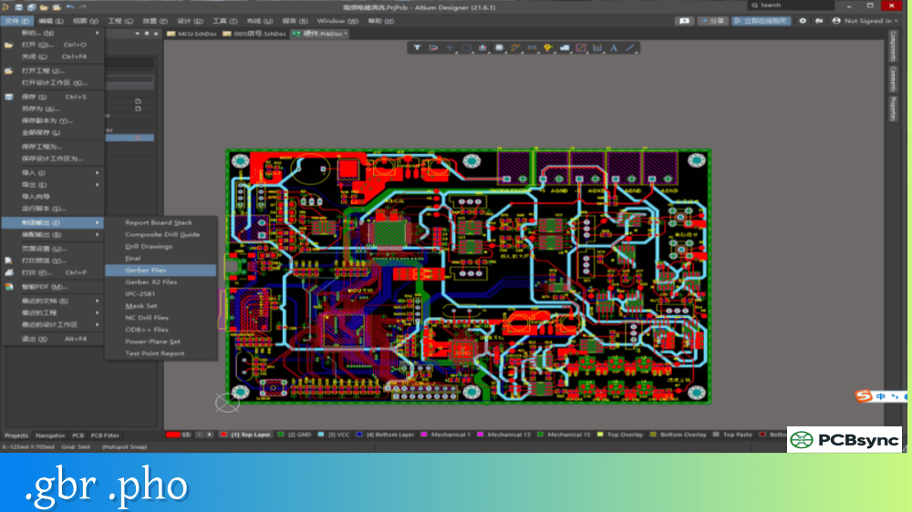
Gerber (RS-274-X)
File → Plot
PCB fabrication
Excellon drill
File → Fabrication Outputs → Drill Files
Drill data
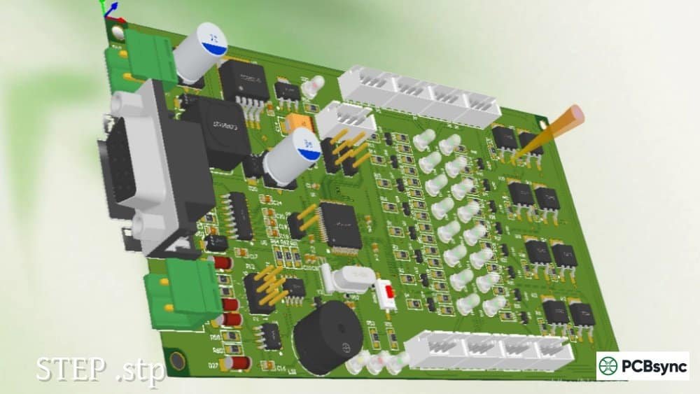
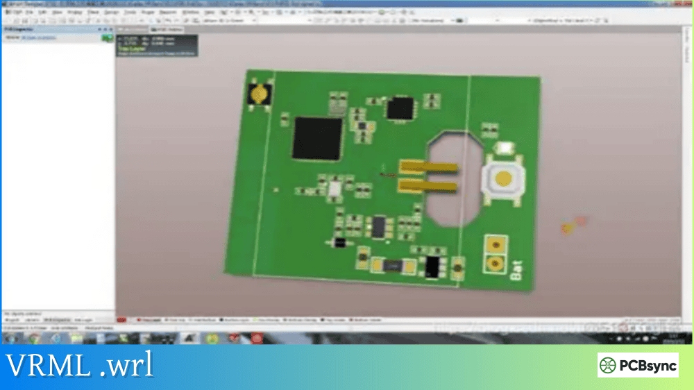
STEP/VRML
File → Export → STEP/VRML
Mechanical CAD integration
DXF
File → Export → DXF
Board outline for MCAD
IPC-D-356
File → Fabrication Outputs
Netlist for testing
PDF
File → Plot (PDF format)
Documentation
Converting to Altium Designer
Altium Designer includes an Import Wizard that directly reads .kicad_pcb files:
In Altium, select File → Import Wizard
Choose KiCad Design Files
Select your .kicad_pcb and .kicad_sch files
Map layers as prompted
Review the migration log for any conversion issues
The conversion typically requires some manual cleanup, but Altium’s importer handles most design elements correctly.
Online Conversion Tools
Tool
URL
Conversion
Futureware Altium2KiCad
www2.futureware.at/KiCad
Altium → KiCad
EasyEDA
easyeda.com
Multiple formats to/from KiCad
Generating Manufacturing Outputs from .kicad_pcb
The .kicad_pcb file is your design database, but PCB manufacturers need Gerber files and drill data. KiCad generates these from the Plot dialog.
Choose Gerber format, enable “Use Gerber X2 attributes”
5
Click Plot to generate files
6
Click Generate Drill Files for Excellon output
7
Verify outputs in KiCad’s Gerber Viewer
Many PCB manufacturers now accept .kicad_pcb files directly, generating their own Gerbers. This can reduce errors from misconfigured exports. Check with your manufacturer whether they support native KiCad file submission.
Because .kicad_pcb files are structured text, they’re amenable to scripting and automation.
Python Scripting with KiCad
KiCad includes Python bindings that allow direct manipulation of PCB data:
python
import pcbnew# Load boardboard = pcbnew.LoadBoard(“mydesign.kicad_pcb”)# Iterate through footprintsfor footprint in board.GetFootprints(): print(f”{footprint.GetReference()}: {footprint.GetPosition()}”)# Save modified boardpcbnew.SaveBoard(“modified.kicad_pcb”, board)
This enables automated tasks like generating panelized boards, updating footprints in batch, or extracting design data for reporting.
Direct Text Manipulation
For simple changes, you can edit .kicad_pcb files directly in a text editor. Common use cases include:
Changing board thickness in the general section
Updating title block information
Bulk find-and-replace on net names
Fixing minor syntax issues from failed imports
Always back up your file before manual editing, and verify the result opens correctly in KiCad.
Version Compatibility
The .kicad_pcb format has evolved with each major KiCad release. Files from newer versions may not open in older KiCad installations.
KiCad Version History
KiCad Version
File Format Changes
4.x
Introduced S-expression .kicad_pcb format
5.x
Added zone fill settings, improved footprint format
6.x
New schematic format, project structure changes
7.x
Custom design rules, improved attributes
8.x
Enhanced stackup definition, new properties
When sharing designs, specify which KiCad version you used. If collaborators have older versions, consider providing Gerber outputs as a fallback.
Useful Resources for .kicad_pcb Files
Official Documentation
Resource
URL
Description
KiCad File Formats
dev-docs.kicad.org/en/file-formats
Official format specification
KiCad Documentation
docs.kicad.org
User manuals and tutorials
KiCad Downloads
kicad.org/download
Latest KiCad releases
Community Resources
Resource
URL
Description
KiCad Forum
forum.kicad.info
Community support and discussions
KiCad GitHub
github.com/KiCad
Source code and issue tracking
Wikibooks KiCad
en.wikibooks.org/wiki/Kicad
Community-maintained documentation
Component Libraries
Resource
Description
SnapEDA
Free symbols and footprints for KiCad
Ultra Librarian
Component library with KiCad export
Digi-Key KiCad Library
Official Digi-Key component library
KiCad Official Libraries
Included with KiCad installation
Frequently Asked Questions About .kicad_pcb Files
Can I open .kicad_pcb files without KiCad installed?
Yes, .kicad_pcb files are plain ASCII text, so any text editor can display the raw content. However, to view the graphical board layout or make design changes, you need KiCad or another EDA tool that supports the format (like EasyEDA or Altium with import). For quick visual inspection without installing KiCad, some online Gerber viewers accept KiCad files, though results vary.
How do I convert .kicad_pcb to Gerber files?
In KiCad’s PCB editor, go to File → Plot. Select your output directory, check the layers you need (typically F.Cu, B.Cu, F.Mask, B.Mask, F.SilkS, B.SilkS, Edge.Cuts), and click Plot. Then click “Generate Drill Files” to create Excellon drill data. Always verify your Gerbers in KiCad’s built-in Gerber Viewer or a standalone viewer before sending to fabrication.
Why won’t my .kicad_pcb file open in an older KiCad version?
The .kicad_pcb format changes between major KiCad releases. Files created in KiCad 7 or 8 contain syntax and features that older versions don’t understand. The solution is either to upgrade to a newer KiCad version, or ask the file creator to export Gerbers or save in a compatible format. KiCad does not provide a “save as older version” option.
Can PCB manufacturers accept .kicad_pcb files directly?
Yes, many manufacturers now accept native .kicad_pcb files and generate Gerbers themselves. This includes popular services like JLCPCB, PCBWay, and Multi-CB. Submitting native files can reduce export errors and allows the manufacturer to optimize settings for their process. However, always confirm with your specific manufacturer what file formats they accept.
How do I fix a corrupted .kicad_pcb file?
Since .kicad_pcb files are text-based, minor corruption is sometimes fixable. Open the file in a text editor and look for obvious syntax errors—mismatched parentheses, truncated lines, or garbled characters. KiCad creates backup files (.kicad_pcb-bak), so check if a recent backup exists. For version-controlled projects, you can also revert to a previous commit. If the file is severely corrupted, you may need to regenerate from schematics or restore from a separate backup.
Conclusion
The .kicad_pcb file format embodies KiCad’s philosophy of openness and transparency. Unlike proprietary binary formats that lock designs into specific tools, the S-expression text format means your PCB data remains accessible, scriptable, and version-controllable indefinitely.
Whether you’re a hobbyist designing your first board or a professional engineer evaluating open-source EDA tools, understanding the .kicad_pcb format helps you work more effectively with KiCad and collaborate smoothly with others in the ecosystem. The format’s readability also makes troubleshooting easier—when something goes wrong, you can often diagnose the issue by examining the file directly.
As KiCad continues gaining professional adoption, the .kicad_pcb format serves as a practical, well-documented standard for PCB design data exchange in the open-source hardware community.
Inquire: Call 0086-755-23203480, or reach out via the form below/your sales contact to discuss our design, manufacturing, and assembly capabilities.
Quote: Email your PCB files to Sales@pcbsync.com (Preferred for large files) or submit online. We will contact you promptly. Please ensure your email is correct.
Notes: For PCB fabrication, we require PCB design file in Gerber RS-274X format (most preferred), *.PCB/DDB (Protel, inform your program version) format or *.BRD (Eagle) format. For PCB assembly, we require PCB design file in above mentioned format, drilling file and BOM. Click to download BOM template To avoid file missing, please include all files into one folder and compress it into .zip or .rar format.


