Inquire: Call 0086-755-23203480, or reach out via the form below/your sales contact to discuss our design, manufacturing, and assembly capabilities.
Quote: Email your PCB files to Sales@pcbsync.com (Preferred for large files) or submit online. We will contact you promptly. Please ensure your email is correct.
Notes: For PCB fabrication, we require PCB design file in Gerber RS-274X format (most preferred), *.PCB/DDB (Protel, inform your program version) format or *.BRD (Eagle) format. For PCB assembly, we require PCB design file in above mentioned format, drilling file and BOM. Click to download BOM template To avoid file missing, please include all files into one folder and compress it into .zip or .rar format.
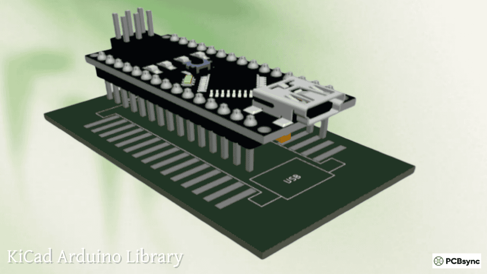
KiCad 3D Integration: Complete Guide to Blender, FreeCAD, Fusion 360 & SolidWorks Workflows
If you’ve spent any time designing PCBs in KiCad, you know the KiCad 3D view is more than just eye candy. It’s become essential for catching mechanical clearance issues, creating professional documentation, and collaborating with mechanical engineers. But here’s the thing: when you need to take your design beyond KiCad’s built-in viewer, the export workflow can get tricky fast.
I’ve spent countless hours figuring out the cleanest ways to get my boards from KiCad to Blender for renders, through KiCad to FreeCAD using KiCadStepUp, and into professional MCAD tools like Fusion 360 and SolidWorks. This guide covers everything I’ve learned about KiCad 3D integration with major CAD platforms.
Why KiCad 3D Integration Matters for PCB Engineers
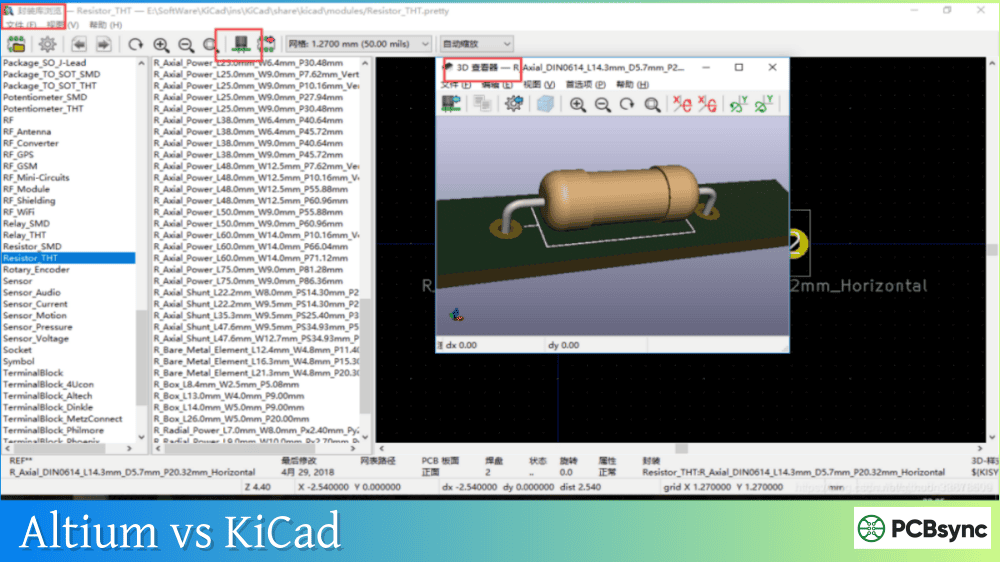
Before diving into workflows, let’s address why this matters. The built-in KiCad 3D view handles quick visualization and basic raytracing pretty well. Hit Alt+3 from PCBnew, and you get an instant preview of your populated board. The problem comes when you need more.
Here’s what the native viewer can’t do:
Generate photorealistic product renders for documentation or marketing
Integrate your PCB into a full mechanical assembly with collision detection
Design enclosures around actual component heights
Export models that your mechanical team can actually use in SolidWorks or Fusion 360
This is where ECAD-MCAD integration becomes critical. Whether you’re a solo maker designing a case or part of a team where electrical and mechanical engineers need to collaborate, getting your PCB into external CAD software is a fundamental skill.
Understanding KiCad’s 3D Export Formats
Before choosing a workflow, you need to understand what KiCad can actually export. The KiCad 3D view relies on two primary file formats in the kicad packages3D library:
Format
Purpose
Contains
Best For
STEP (.step, .stp)
MCAD integration
Solid geometry, dimensions
Fusion 360, SolidWorks, FreeCAD
VRML (.wrl)
Visualization
Colored meshes, materials
Blender, raytracing renders
STEP files are the industry standard for mechanical CAD exchange. They contain solid body geometry with proper scaling and can be manipulated in any professional CAD package. However, STEP exports from KiCad don’t include copper traces, silkscreen graphics, or soldermask colors.
VRML files (.wrl) are essentially colored meshes optimized for the KiCad 3D viewer’s raytracing engine. They look great in KiCad but aren’t directly compatible with most MCAD software. Blender can import them via the X3D importer.
The kicad packages3D Library
The official kicad packages3D repository contains thousands of 3D models for common components. Each footprint in KiCad’s standard library has both STEP and WRL versions linked. You can find the complete library at:
If you’re building custom footprints, you’ll want to create both STEP and WRL versions of your 3D models. The STEP file should be 1:1 in millimeters, while WRL files use KiCad’s normalized units (0.1 inches).
KiCad to FreeCAD: The KiCadStepUp Workflow
For serious ECAD-MCAD collaboration, the KiCadStepUp workbench is the gold standard. This FreeCAD addon creates a bidirectional link between KiCad and FreeCAD, letting you push and pull designs between the two programs.
What KiCadStepUp Actually Does
KiCadStepUp isn’t just an importer. It’s a full collaboration tool that enables:
Loading .kicad_pcb files directly into FreeCAD with all components
Exporting populated boards to STEP or IGES format
Pushing and pulling PCB edge cuts between KiCad and FreeCAD’s Sketcher
Syncing 3D model positions between both programs
Checking interference between enclosures and components
Converting STEP models to properly-scaled VRML for use in KiCad
Installing KiCadStepUp
The installation process has gotten much simpler. In FreeCAD 0.17 and later:
Open FreeCAD
Go to Tools → Addon Manager
Search for “KiCadStepUp”
Click Install
Restart FreeCAD
After installation, configure the workbench by setting your KiCad 3D model paths. In FreeCAD’s preferences, navigate to KiCadStepUp and set the path to your kicad packages3D folder (typically found at the KICAD6_3DMODEL_DIR or KICAD7_3DMODEL_DIR environment variable location).
Step-by-Step: KiCad to FreeCAD Export
Here’s my standard workflow for getting a clean STEP export:
Step 1: Load Your Board
In FreeCAD with the KiCadStepUp workbench active, click the “Load Board” icon and select your .kicad_pcb file. FreeCAD will parse the board outline, place all footprints, and load the associated 3D models.
Step 2: Load Copper and Silkscreen (Optional)
For visualization, you can load copper traces and silkscreen layers. Click the appropriate toolbar icons and select your .kicad_pcb file again. Note that complex boards can take several minutes to process.
Step 3: Export to STEP
Select the top-level compound in FreeCAD’s model tree, then go to File → Export and choose STEP format. This produces a single STEP file containing your entire populated PCB assembly.
Advanced KiCadStepUp Features
One underused feature is the PCB edge push/pull functionality. If your mechanical engineer needs to adjust the board outline to fit an enclosure, they can modify it in FreeCAD’s Sketcher and push the changes back to your .kicad_pcb file. This works in reverse too, so layout changes propagate to the mechanical design.
For footprint designers, KiCadStepUp can load .kicad_mod files directly, making it easy to align 3D models precisely with pad positions.
KiCad to Blender: Photorealistic PCB Rendering
When you need stunning product renders, Blender is the way to go. The KiCad to Blender workflow has improved dramatically with the pcb2blender plugin.
Traditional Method: VRML Export
The old-school approach works like this:
In KiCad PCBnew, go to File → Export → VRML
In Blender, use File → Import → X3D Extensible 3D
Set Forward to “X Forward” and Up to “Z Up”
Import your .wrl file
This method gets your board into Blender with colors intact, but you lose copper trace detail and the soldermask doesn’t always render correctly. The VRML export doesn’t faithfully represent mask openings over copper.
Modern Method: pcb2blender Plugin
The pcb2blender workflow from developer 30350n is now the preferred method for KiCad Blender integration. It creates a dedicated .pcb3d format that preserves much more detail.
Installation:
In KiCad, install the exporter via Tools → Plugin and Content Manager, search for pcb2blender. For Blender, download the importer from GitHub (https://github.com/30350n/pcb2blender) and install via Edit → Preferences → Add-ons → Install from Disk.
Workflow:
In KiCad PCBnew, click “Export to Blender (.pcb3d)”
In Blender, go to File → Import → PCB (.pcb3d)
Start composing your scene
The plugin comes with pre-configured PCB shaders that simulate soldermask, copper, FR4 substrate, and silkscreen materials. You can customize colors and surface properties to match your actual fab specifications.
Creating Realistic Materials in Blender
For truly photorealistic renders, you’ll want to fine-tune materials:
PCB Element
Blender Material Settings
Soldermask
Glossy shader, slight subsurface scattering, typical colors: green (#008000), matte black (#1a1a1a), red (#cc0000)
HASL Solder
Metallic shader, silver color (#c0c0c0), medium roughness
ENIG Gold
Metallic shader, gold color (#d4af37), low roughness
Matte diffuse, white (#ffffff) or yellow (#ffff00)
The key to realistic PCB renders is getting the soldermask right. Real soldermask has some translucency, so a pure glossy green looks fake. Add slight subsurface scattering to simulate light passing through the mask layer.
KiCad to Fusion 360: STEP Export Workflow
Fusion 360 has become popular among hobbyists and professionals alike, making KiCad Fusion 360 integration a common need. Recent versions of Fusion 360 can import KiCad files directly, but the STEP workflow remains the most reliable.
Direct STEP Export Method
This is the simplest approach:
Ensure all components in your design have STEP models assigned (check in the 3D viewer)
In PCBnew, go to File → Export → STEP
Keep default settings (board origin, substitute models with default shapes)
Click Export
The resulting .step file can be opened directly in Fusion 360 via File → Open → Open from my computer.
Importing into an Existing Fusion 360 Assembly
If you’re designing an enclosure and need to import the PCB:
Open Fusion 360 and save your STEP file to a project
In your assembly, right-click the project name
Select “New Component”
Drag the PCB from “My Recent Data” into the new component
The PCB is now a proper component in your assembly with full collision detection.
Limitations of KiCad to Fusion 360 Direct Export
The STEP export preserves geometry and basic colors, but has limitations:
No copper trace graphics on the board surface
Via holes may not export cleanly
Silkscreen text isn’t visible
Surface finish details are lost
For renders that show these details, you need the workaround of using tracespace-cli to generate layer graphics, then applying them as textures in Fusion 360’s rendering workspace. This is well documented in various tutorials but adds significant complexity.
Fusion 360 Native KiCad Import
Autodesk has added experimental KiCad import capability to Fusion 360. Check Help → What’s New for current support status. This feature reads .kicad_pcb files directly but may not support all KiCad versions.
KiCad to SolidWorks: Professional MCAD Integration
SolidWorks is the industry standard for mechanical engineering, so KiCad SolidWorks workflows are critical for professional teams. The process is similar to Fusion 360 but with some SolidWorks-specific considerations.
Basic STEP Import
The straightforward method:
Export STEP from KiCad as described above
In SolidWorks, use File → Open and select the .step file
SolidWorks will import it as a multibody part or assembly
Dealing with Import Issues
Users sometimes report problems with STEP imports in SolidWorks, such as components appearing with wrong geometry or the model tree showing errors. Common fixes:
Problem
Solution
Components display incorrectly
Try importing through FreeCAD first, then re-export to STEP
Missing bodies in feature tree
Check that all KiCad 3D models are proper solid bodies, not surfaces
Assembly relationships broken
Import as “Part” rather than “Assembly”
File won’t open
Update to latest KiCad version, STEP export has improved significantly
Alternative: DXF Layer Export
For cases where you need pad locations or silkscreen for mating features:
This hybrid approach gives you precise pad locations for connector cutouts while maintaining the full 3D assembly from STEP.
SolidWorks Collision Detection with PCB Assemblies
One major benefit of importing into SolidWorks is interference detection. After importing your PCB:
Insert it into your enclosure assembly
Go to Evaluate → Interference Detection
Select all components and calculate
SolidWorks will highlight any collisions between enclosure features and PCB components, catching issues that would be expensive to find after fabrication.
Before any export workflow, you need a properly configured KiCad 3D view. Here are the essentials:
Verifying 3D Model Coverage
Open the 3D viewer (Alt+3) and visually inspect your board. Missing models appear as simple colored boxes or nothing at all. For each missing model:
Hover over the component in PCBnew and press E to edit
Navigate to the 3D Settings tab
Add the appropriate STEP and/or WRL file
Adjust offset, rotation, and scale as needed
Raytracing Settings
KiCad’s raytracer has improved significantly. For best results:
Enable raytracing via the toolbar icon (blue 3D cube)
Adjust light settings under Preferences → 3D Viewer → Raytracing
Set soldermask color to match your actual fab specification
Enable floor plane for more realistic shadows
The raytracer is CPU-intensive but produces excellent results for documentation screenshots.
Custom 3D Model Sources
When the kicad packages3D library doesn’t have what you need:
Source
Description
Format
Manufacturer websites
Often provide STEP files for their components
STEP
GrabCAD
Large community library of 3D models
Various
SnapEDA
PCB-focused library with matched footprints
STEP, WRL
3D Content Central
Dassault-hosted model library
STEP
Component Search Engine
Searches multiple sources
STEP
When using third-party models, verify that the dimensions match your footprint. Scaling issues are a common source of mechanical fit problems.
Practical Comparison: Which Workflow to Use
Based on my experience, here’s when to use each approach:
Use Case
Recommended Workflow
Quick enclosure design, hobbyist
KiCad → STEP → Fusion 360
Professional MCAD collaboration
KiCad → KiCadStepUp → STEP → SolidWorks
Product photography / marketing
KiCad → pcb2blender → Blender
Bidirectional design iteration
KiCad ↔ KiCadStepUp ↔ FreeCAD
Complex multi-board systems
KiCad → FreeCAD → merge → STEP
The KiCadStepUp workflow through FreeCAD adds an extra step but gives you the most flexibility for professional use. The direct STEP export works fine for simpler needs.
Useful Resources and Downloads
Here are the essential resources for KiCad 3D integration:
Why doesn’t my STEP export include copper traces and silkscreen?
The STEP export from KiCad only includes solid 3D geometry: the board substrate and component models. Copper traces, silkscreen, and soldermask are 2D graphics applied to the board surface. For MCAD purposes, the solid geometry is what matters for fit and clearance. If you need surface details for rendering, use the VRML export or the pcb2blender workflow for Blender, or apply gerber-generated textures in your rendering software.
My components appear as boxes in the 3D viewer. How do I fix this?
This happens when KiCad can’t find the 3D models for your footprints. First, verify your library paths are correct in Preferences → Configure Paths. The KICAD_3DMODEL_DIR variable should point to your kicad packages3D folder. For custom footprints, you need to manually assign 3D models in the footprint properties (3D Settings tab). If you’re using third-party libraries, they may not include 3D models at all.
KiCadStepUp takes forever to load my board. Is this normal?
Complex boards with many unique components can take several minutes to load, especially the first time when FreeCAD is caching models. Boards with custom board outlines containing many vertices or complex copper fills are particularly slow. If loading consistently takes more than 10-15 minutes, try simplifying your board outline or loading without copper layers initially. Some users report that board outline cleanup in KiCad significantly improves load times.
Can I edit the PCB in Fusion 360 or SolidWorks and send changes back to KiCad?
Not directly. The STEP export is a one-way transfer of geometry. However, KiCadStepUp does support bidirectional editing of board outlines between KiCad and FreeCAD. You can modify the Edge.Cuts layer in FreeCAD’s Sketcher and push changes back to your .kicad_pcb file. For full electrical-mechanical collaboration, this is the recommended workflow rather than trying to edit in Fusion 360 or SolidWorks.
What’s the difference between STEP and VRML models in KiCad?
STEP files contain solid geometry with precise dimensions and are intended for mechanical CAD integration. VRML files contain colored meshes optimized for visualization and rendering. KiCad uses STEP files when exporting for MCAD and VRML files for its internal 3D viewer’s raytracing. A properly configured kicad packages3D component has both files with matching geometry. When creating custom models, you should provide both formats: STEP for mechanical accuracy and VRML for appearance in the KiCad 3D view.
Troubleshooting Common Issues
Even with proper setup, you’ll encounter occasional problems. Here are solutions to the most common issues I’ve run into.
Model Scaling Problems
Models appearing too large or small is usually a units mismatch. KiCad expects STEP files in millimeters at 1:1 scale. VRML files should be normalized to 0.1 inch units. When importing third-party models, check the original units and apply the appropriate scale factor in the footprint 3D settings.
Missing or Incorrect Colors After Export
STEP files don’t preserve material colors the same way VRML does. When importing STEP into Fusion 360 or SolidWorks, you may need to manually reassign materials. For Blender workflows, stick with VRML or pcb2blender exports which maintain color information.
Board Outline Issues
If your exported board has the wrong shape or missing cutouts, check your Edge.Cuts layer in KiCad. All outline segments must form closed polygons with no gaps. Use the Design Rule Checker to verify outline integrity before export.
Conclusion: Building an Efficient 3D Workflow
Getting KiCad 3D integration right takes some upfront investment, but it pays dividends in fewer mechanical surprises during assembly. My recommendation for anyone serious about ECAD-MCAD collaboration:
Start with the native KiCad 3D view for quick checks during layout. Set up KiCadStepUp in FreeCAD for your production workflow, especially if you’re working with mechanical engineers. When you need renders, the KiCad to Blender pipeline via pcb2blender produces results that would have required expensive commercial tools just a few years ago.
The key is keeping your kicad packages3D library updated and ensuring every footprint has proper 3D models assigned. Once that foundation is in place, exporting to any platform becomes straightforward.
Whether you’re doing KiCad to FreeCAD transfers for enclosure design, KiCad Fusion 360 imports for hobbyist projects, or full KiCad SolidWorks integration for professional work, the workflows covered here will get you there.
Inquire: Call 0086-755-23203480, or reach out via the form below/your sales contact to discuss our design, manufacturing, and assembly capabilities.
Quote: Email your PCB files to Sales@pcbsync.com (Preferred for large files) or submit online. We will contact you promptly. Please ensure your email is correct.
Notes: For PCB fabrication, we require PCB design file in Gerber RS-274X format (most preferred), *.PCB/DDB (Protel, inform your program version) format or *.BRD (Eagle) format. For PCB assembly, we require PCB design file in above mentioned format, drilling file and BOM. Click to download BOM template To avoid file missing, please include all files into one folder and compress it into .zip or .rar format.


