Inquire: Call 0086-755-23203480, or reach out via the form below/your sales contact to discuss our design, manufacturing, and assembly capabilities.
Quote: Email your PCB files to Sales@pcbsync.com (Preferred for large files) or submit online. We will contact you promptly. Please ensure your email is correct.
Notes: For PCB fabrication, we require PCB design file in Gerber RS-274X format (most preferred), *.PCB/DDB (Protel, inform your program version) format or *.BRD (Eagle) format. For PCB assembly, we require PCB design file in above mentioned format, drilling file and BOM. Click to download BOM template To avoid file missing, please include all files into one folder and compress it into .zip or .rar format.
If you’ve been designing PCBs for a while, you know that IoT projects hit different. I’ve spent over a decade working on circuit boards across consumer electronics, industrial automation, and smart devices—and I can tell you that IoT PCB design comes with challenges you simply don’t encounter in traditional board work.
The Internet of Things has fundamentally changed how we approach printed circuit board design. We’re no longer just routing traces and placing components; we’re building the nervous system of an interconnected world. From the smart thermostat in your living room to industrial sensors monitoring factory equipment 24/7, IoT PCBs are everywhere—and they demand a different mindset.
In this guide, I’ll walk you through everything I’ve learned about designing, manufacturing, and optimizing IoT PCBs. Whether you’re transitioning from traditional PCB work or starting fresh in the IoT space, you’ll find actionable insights that actually work in real-world projects.
An IoT PCB (Internet of Things Printed Circuit Board) is a specialized circuit board designed to enable smart, connected devices. Unlike conventional PCBs that simply provide electrical connections between components, IoT PCBs integrate sensors, wireless communication modules, microcontrollers, and power management systems—all optimized for network connectivity and data exchange.
Think of it this way: a traditional PCB is like a standalone calculator. An IoT PCB is more like a smartphone—it’s not just processing information locally but constantly communicating with the outside world.
Key Characteristics of IoT PCBs
What sets IoT PCBs apart from conventional boards? Here’s what I consistently see across successful IoT designs:
Compact Form Factor: Most IoT devices need to fit into tight spaces. We’re talking about boards that might need to squeeze into a wearable band or sit behind a smart switch plate.
Wireless Connectivity: Every IoT PCB needs some form of wireless communication—whether that’s Wi-Fi, Bluetooth, Zigbee, LoRa, or cellular. This introduces RF design considerations that many PCB engineers haven’t dealt with before.
Low Power Operation: Battery life is king in IoT. Many devices need to run for months or even years on a single charge, which means every microamp matters.
Sensor Integration: IoT devices collect data from the physical world, so they typically include multiple sensors for temperature, humidity, motion, light, or other environmental parameters.
Security Features: Connected devices are potential attack vectors. Modern IoT PCBs often include hardware encryption, secure boot capabilities, and tamper detection.
IoT PCB Design: Core Requirements and Considerations
When I start a new IoT PCB project, I always begin with a requirements checklist. Missing something at the design stage means expensive respins later. Here’s what you need to nail down before laying out your first trace.
Size and Miniaturization
IoT devices are shrinking. The market demands smaller, sleeker products, but the functionality expectations keep growing. This creates a real tension in PCB design.
High-Density Interconnect (HDI) technology has become essential for serious IoT work. HDI uses finer lines, smaller vias, and higher component density to pack more functionality into less space. If you’re designing a wearable or a compact smart sensor, you’ll almost certainly need HDI techniques.
Some strategies that work well for miniaturization:
Using System-in-Package (SiP) components that integrate multiple functions on a single chip dramatically reduces board real estate. For example, a single SiP module might combine your MCU, power management, and RF frontend.
Multilayer PCBs let you route signals on internal layers, freeing up surface area for components. Most IoT designs I work on are 4-6 layers minimum.
Surface Mount Technology (SMT) components are standard, but you’ll want to push toward smaller packages (0402 or even 0201 passives) where your assembly process supports it.
Wireless Connectivity Requirements
Choosing the right wireless protocol is one of the most critical decisions in IoT PCB design. Each has trade-offs in terms of range, power consumption, data rate, and complexity.
Protocol
Range
Data Rate
Power Consumption
Best For
Wi-Fi
50-100m
Up to 1 Gbps
High
High-bandwidth, always-powered devices
Bluetooth LE
10-100m
1-2 Mbps
Low
Wearables, proximity sensing
Zigbee
10-100m
250 Kbps
Very Low
Smart home, mesh networks
LoRa
2-15 km
0.3-50 Kbps
Very Low
Long-range sensors, agriculture
NB-IoT
Cellular
250 Kbps
Low
Wide-area IoT, remote monitoring
Thread
10-100m
250 Kbps
Low
Smart home, Matter ecosystem
Wi-Fi HaLow (802.11ah)
Up to 1 km
150 Kbps-78 Mbps
Moderate
Smart building, outdoor IoT
When designing for wireless connectivity, remember that the module is only part of the equation. Your PCB layout directly impacts wireless performance. I’ve seen well-designed RF modules perform terribly because of poor PCB implementation, and I’ve seen cheaper modules excel because of careful attention to layout.
Antenna design and placement deserve serious attention. A poorly placed antenna can kill your wireless performance. Keep antennas away from metal objects, batteries, and high-frequency digital circuits. Most antenna manufacturers provide reference designs and keepout specifications—follow them religiously.
For PCB antennas (printed directly on the board), work closely with your antenna vendor or use their proven reference designs. The relationship between antenna geometry, ground plane shape, and surrounding components is complex, and small changes can have significant impacts. Many engineers underestimate this and spend weeks debugging range issues that could have been avoided.
Consider using external antennas for applications where range is critical or the enclosure presents challenges. External antennas give you more flexibility and often better performance, though they add cost and assembly complexity.
Power Management Strategies
Power efficiency isn’t just a nice-to-have in IoT—it’s often the make-or-break factor for product viability. Here’s how I approach it:
Component Selection: Start with low-power MCUs designed for IoT applications. Parts like the Nordic nRF52 series, ESP32 variants, or STM32L family are built from the ground up for low-power operation.
Sleep Modes: Design your system to spend most of its time in deep sleep. A well-designed IoT sensor might be active for only milliseconds at a time, sleeping the rest.
Efficient Voltage Regulation: Use DC-DC converters with good efficiency at light loads, or LDOs with very low quiescent current (under 1 μA for the best parts). Every microamp counts when you’re running on a coin cell.
Power Gating: Completely disconnect power from unused peripherals. Don’t just put them in sleep mode—cut the power entirely.
Energy Harvesting: For some applications, solar cells, vibration harvesting, or thermal energy scavenging can extend battery life dramatically or even enable battery-free operation.
Thermal Management
IoT devices often operate in thermally challenging environments—think of an industrial sensor in a hot factory or a smart streetlight baking in the sun. At the same time, their compact size limits heat dissipation options.
Key thermal design considerations include:
Strategic component placement to distribute heat sources across the board rather than concentrating them. Thermal vias under hot components to conduct heat to internal copper planes. Heat spreading using copper pours on multiple layers. Careful calculation of thermal budgets during the design phase—don’t leave thermal design until you have a problem.
IoT PCB Materials: Choosing the Right Substrate
Material selection impacts everything from signal integrity to long-term reliability. Here’s a breakdown of the most common materials for IoT applications.
FR-4: The Workhorse Material
FR-4 is the standard PCB material for good reason. It’s cost-effective, widely available, and works well for most IoT applications. Standard FR-4 offers:
A dielectric constant (Dk) around 4.0-4.4, which is adequate for most sub-GHz applications. Operating temperature up to 130-140°C for standard grades. Good mechanical strength and dimensional stability. Excellent manufacturer familiarity and process support.
For many IoT designs—especially those in controlled environments—FR-4 is perfectly adequate.
Polyimide: When Flexibility Matters
Polyimide is the go-to material for flexible and rigid-flex PCBs. If your IoT device needs to bend, fold, or conform to curved surfaces, polyimide is likely your answer.
Property
FR-4
Polyimide
Flexibility
Rigid
Highly flexible
Dk (Dielectric Constant)
4.0-4.4
3.2-3.5
Max Operating Temp
130-140°C
260-300°C
Cost
Lower
Higher
Moisture Absorption
0.1%
Up to 2%
Typical Thickness
0.8-1.6mm
0.05-0.3mm
Best Applications
General IoT, fixed installations
Wearables, medical devices, space-constrained designs
Polyimide shines in wearables, medical implants, and any application where the board needs to survive repeated flexing. The higher temperature resistance also makes it valuable for harsh-environment IoT deployments.
High-Frequency Materials
For IoT devices operating at higher frequencies (think 2.4 GHz Wi-Fi, 5 GHz bands, or cellular), you may need specialized materials:
Rogers materials (like RO4350B) offer lower Dk and loss tangent, which is crucial for RF performance. They’re commonly used for the RF portion of mixed-technology boards.
PTFE (Teflon) provides excellent high-frequency performance but is more difficult to process and more expensive.
A common approach in IoT design is using hybrid stackups—FR-4 for digital sections and high-frequency material for RF sections. This balances performance against cost.
Ceramic PCBs
For extreme environments or very high thermal loads, ceramic PCBs (typically aluminum nitride or alumina) offer exceptional thermal conductivity and reliability. They’re expensive and reserved for specialized applications like high-power LED drivers or automotive IoT modules.
After working on dozens of IoT projects, I’ve developed a set of practices that consistently lead to successful designs. Here’s what actually works.
Before diving into layout, spend time on a thorough design review. Get other engineers to look at your schematic, question your component choices, and challenge your assumptions. The cost of finding a problem in schematic review is tiny compared to finding it after boards are built.
Create a design checklist specific to IoT. Include items like: Is the antenna keepout defined? Are all power rails properly decoupled? Is the RF section isolated from noisy digital circuits? Have I met the reference design requirements for all modules? Check every item before releasing to layout.
Layout and Component Placement
Good placement is 80% of good routing. Get this wrong, and you’ll fight the layout the entire way through.
Group by function: Keep analog circuits separate from digital, RF sections isolated, and power components together. This isn’t just about convenience—it’s about signal integrity and EMI control.
Prioritize the RF path: If you’re using wireless connectivity, the antenna and RF frontend should drive your placement decisions. RF traces need to be as short as possible with controlled impedance.
Consider the thermal map: Identify your hot spots early and place heat-generating components where they can dissipate effectively.
Plan for testability: Include test points for critical signals. You’ll thank yourself during bring-up and production test.
Signal Integrity for IoT PCBs
Signal integrity challenges in IoT come from two directions: the high-speed digital buses (SPI, I2C, USB) connecting your MCU to peripherals, and the RF circuits handling wireless communication.
For digital signals:
Keep trace lengths as short as possible, especially for high-speed interfaces. Use ground planes on adjacent layers to provide a solid return path. Match trace impedance to source and load—typically 50Ω for single-ended, 100Ω for differential pairs. Avoid routing high-speed signals near board edges or across plane splits.
For RF circuits:
Maintain 50Ω impedance for antenna feeds (or whatever your RF design requires). Use generous ground clearance around RF traces. Keep digital signals away from RF sections—crosstalk here kills wireless performance. Follow your RF module manufacturer’s reference design exactly unless you really know what you’re doing.
EMI/EMC Considerations
IoT devices must meet regulatory requirements (FCC, CE, etc.), and EMI issues are one of the most common reasons for certification failure. Address EMI proactively:
Proper grounding: A solid ground plane is your first line of defense. Multi-layer stackups with dedicated ground planes work best.
Filtering: Add appropriate filtering on power inputs and any signals crossing between functional blocks.
Shielding: For sensitive RF circuits, consider metal shields or shielding cans. Many RF modules are designed to work with standard shield can footprints.
Clock management: Your system clock is a major EMI source. Keep clock traces short, use series termination resistors, and consider spread-spectrum clocking if available.
Design for Manufacturing (DFM)
An IoT PCB that can’t be manufactured economically is useless. Keep these DFM principles in mind:
Use standard via sizes and trace widths where possible. Exotic features cost more and limit your supplier options.
Provide adequate clearance for assembly equipment. Even with small components, don’t crowd things so tightly that pick-and-place machines struggle.
Include fiducials for optical alignment during assembly. Most assemblers need at least two, preferably three.
Design your panelization thoughtfully. Efficient panel utilization reduces manufacturing cost per board.
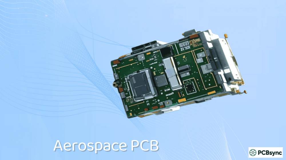
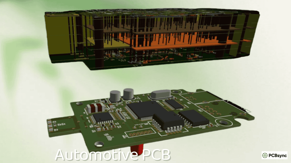
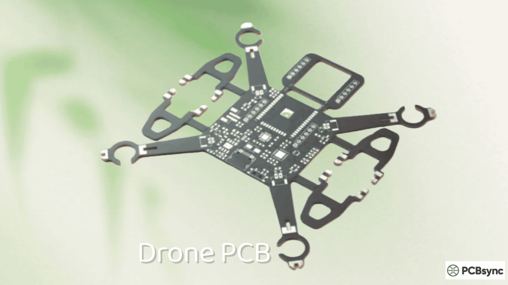
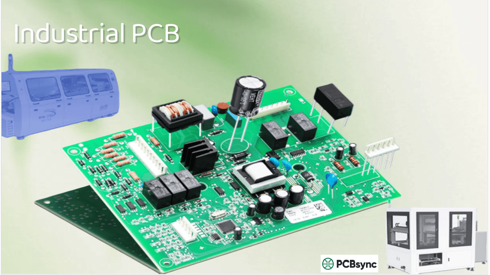
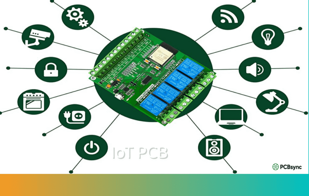
IoT PCB Applications Across Industries
IoT PCBs power connected devices across virtually every industry. Here’s how the requirements differ based on application.
Smart Home Devices
Smart thermostats, lighting controllers, security cameras, and voice assistants all rely on IoT PCBs. These applications typically prioritize:
Cost sensitivity (consumer price points are competitive), aesthetic constraints (boards often need to fit into sleek enclosures), Wi-Fi or Bluetooth connectivity for smartphone integration, and moderate power efficiency since most are wall-powered.
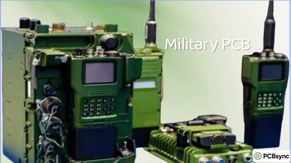
Industrial IoT (IIoT)
Factory automation, predictive maintenance, and process monitoring demand robust IoT PCBs that can handle:
Wide temperature ranges (often -40°C to +85°C or beyond), vibration and mechanical shock, long operational lifetimes (10+ years), and industrial communication protocols (WirelessHART, Zigbee, proprietary).
Conformal coating is almost always required for industrial applications to protect against dust, moisture, and chemical exposure.
Wearable Technology
Fitness trackers, smartwatches, and medical wearables push IoT PCB design to the limits:
Extreme miniaturization using HDI and flexible PCBs, very low power consumption for acceptable battery life, biocompatibility considerations for skin-contact devices, and high reliability despite constant flexing and movement.
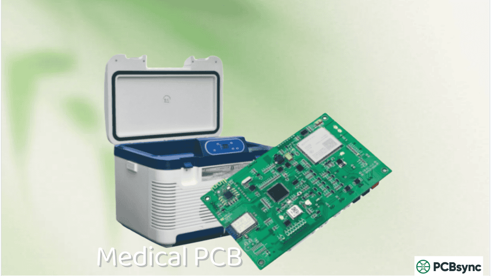
Healthcare and Medical IoT
Medical IoT devices face unique challenges:
Regulatory compliance (FDA, IEC 60601), patient safety and data security requirements, precision sensing for accurate health data, and long-term reliability for implantable or critical-care devices.
Agricultural IoT
Smart agriculture uses IoT sensors for soil monitoring, crop health, and livestock tracking:
Very long battery life (often years) for remote deployment, extreme weather resistance, long-range connectivity (LoRa, NB-IoT) for coverage over large areas, and low cost for deployment at scale.
IoT PCB Manufacturing Process
Understanding the manufacturing process helps you design boards that can actually be built. Here’s the typical flow for IoT PCB production.
When selecting a manufacturing partner for IoT PCBs, consider their capabilities carefully. Not every fab house can handle the fine features HDI demands, and not every assembly shop has experience with the small components and RF modules common in IoT designs. Ask potential partners about their minimum trace/space capabilities, via sizes, layer counts, and experience with your specific type of product.
Turnaround time matters too. IoT development cycles are often fast, and waiting weeks for prototype boards can kill momentum. Many manufacturers now offer quick-turn services (2-5 days for bare boards), but assembly adds time. Plan your schedule accordingly.
Design to Fabrication
Once your design is complete, you’ll generate manufacturing files:
Gerber files define each layer of the PCB Drill files specify hole locations and sizes Bill of Materials (BOM) lists all components Pick and place files define component locations for assembly
Most manufacturers expect Gerber RS-274X format, though some newer systems support ODB++ or IPC-2581.
PCB Fabrication Steps
The basic fabrication sequence includes:
Material preparation and cutting, inner layer imaging and etching, layer lamination, drilling (mechanical and/or laser for microvias), plating of through-holes and vias, outer layer imaging and etching, solder mask application, silkscreen printing, surface finish application (ENIG, HASL, OSP, etc.), and electrical testing.
For HDI boards, this process may repeat multiple times to build up sequential layers.
Assembly Considerations
IoT PCB assembly typically uses SMT (Surface Mount Technology) with some through-hole components where needed:
Solder paste application via stencil, component placement using pick-and-place machines, reflow soldering, inspection (AOI, X-ray for BGAs), through-hole assembly if required, functional testing, and conformal coating if specified.
For IoT products, you’ll likely also have programming steps for MCU firmware and wireless module configuration.
Testing and Quality Assurance
Testing IoT PCBs requires more than just checking electrical connectivity. A comprehensive test strategy includes:
In-Circuit Testing (ICT): Verifies component placement and solder quality. Essential for volume production.
Functional Testing: Validates that the board performs its intended functions—sensors read correctly, wireless communication works, power consumption matches specifications.
RF Testing: Measures wireless performance including transmit power, receiver sensitivity, and antenna pattern. This often requires specialized equipment.
Environmental Testing: Validates operation across temperature, humidity, and vibration ranges for your target application.
Burn-In Testing: For high-reliability applications, extended operation under stress conditions catches early failures.
Document your test procedures thoroughly. Good test documentation saves time in production and helps with troubleshooting when issues arise.
IoT PCB Security Considerations
Connected devices are attack targets. Hardware security should be designed in from the start, not bolted on later.
Hardware Security Features
Modern IoT designs should consider:
Secure elements: Dedicated security ICs like ATECC608A or SE050 provide hardware-based key storage and cryptographic operations.
Secure boot: Ensure only authenticated firmware can run on your device.
Debug port protection: Disable JTAG/SWD in production or implement authentication.
Tamper detection: For high-security applications, include physical tamper switches or sensors.
PCB-Level Security
At the board level, you can make reverse engineering and tampering more difficult:
Use inner layers for sensitive traces, making probing harder. Avoid clear labeling of test points and debug interfaces. Consider potting or conformal coating to obscure components. Implement anti-counterfeiting measures for your own supply chain protection.
Common IoT PCB Design Mistakes to Avoid
I’ve seen these mistakes repeatedly over the years. Learn from others’ pain:
Underestimating antenna requirements: Don’t assume the antenna will “just work.” RF design requires attention, and antenna placement relative to ground planes and metal objects matters enormously.
Ignoring thermal analysis: “It’ll be fine” is not a thermal strategy. Run at least basic thermal simulations, especially for enclosed devices.
Inadequate power budgeting: Calculate your actual power consumption in every operating state. That sleep current you ignored? It’s draining your battery.
Missing bypass capacitors: Every power pin needs appropriate decoupling. This is PCB Design 101, but I still see it missed on IoT boards.
Routing high-speed signals carelessly: USB, SPI, and other high-speed buses need controlled impedance routing. Don’t just “get the traces connected.”
Forgetting regulatory requirements: FCC/CE certification isn’t optional. Design with EMI in mind from the start, or plan for expensive redesigns.
Future Trends in IoT PCB Design
The IoT PCB landscape continues to evolve. Here’s what I’m watching:
AI at the edge: More processing is moving onto IoT devices themselves, driving demand for more powerful MCUs and better thermal management.
5G integration: As 5G IoT modules become more affordable, we’ll see higher bandwidth applications in industrial and consumer IoT.
Ultra-low-power technologies: New MCU architectures and power management techniques are pushing battery life beyond what seemed possible a few years ago.
Advanced packaging: System-in-Package (SiP) and chiplet architectures will enable even smaller, more integrated IoT solutions.
Sustainable design: There’s growing pressure for recyclable materials, reduced energy consumption, and longer product lifespans.
Useful Resources for IoT PCB Designers
Design Tools and Software
KiCad – Free, open-source PCB design tool with an excellent community: https://www.kicad.org/
Altium Designer – Professional PCB design software widely used in industry: https://www.altium.com/
What makes IoT PCB design different from regular PCB design?
IoT PCB design adds several layers of complexity beyond traditional board work. You’re integrating wireless connectivity, which introduces RF design challenges and antenna considerations. Power management becomes critical since many IoT devices run on batteries for extended periods. The form factors are often smaller, requiring HDI techniques. And you must consider security at the hardware level since these devices connect to networks. In traditional PCB design, you might route some signals and call it done. In IoT, you’re balancing wireless performance, battery life, thermal constraints, and security—all in a smaller package.
How do I choose between FR-4 and polyimide for my IoT PCB?
The choice depends on your application requirements. Use FR-4 when your device is in a fixed form factor, operates in moderate temperatures (below 130°C), and cost is a primary concern. Choose polyimide when you need flexibility (wearables, medical devices that conform to body shapes), high-temperature operation (above 150°C), or very thin boards. For many IoT projects, standard FR-4 works fine. But if your device needs to bend, survive extreme heat, or fit into unusual shapes, polyimide is worth the additional cost.
What are the most common causes of IoT PCB failures?
From my experience, the top failure modes are: poor antenna performance due to bad placement or inadequate ground plane design; thermal issues from underestimating heat generation in compact enclosures; power supply problems including excessive noise or inadequate decoupling; ESD damage from insufficient protection on exposed interfaces; and solder joint failures in products subjected to thermal cycling or vibration. Most of these are preventable with proper upfront design attention. The key is not to optimize just for initial function but for long-term reliability in real operating conditions.
How many layers should my IoT PCB have?
For simple IoT devices with basic connectivity (like a Bluetooth sensor node), you might get away with 2 layers, though 4 is more comfortable. For Wi-Fi devices or anything with significant digital complexity, 4-6 layers is typical. High-performance designs with multiple RF paths, complex power management, or high-speed interfaces often need 6-8 layers or more. The decision comes down to routing density, signal integrity requirements, and EMI management needs. More layers cost more, but trying to squeeze a complex design into too few layers creates headaches and often ends up costing more through redesigns and EMI failures.
What certifications do IoT PCBs need?
In the United States, any IoT device with wireless functionality needs FCC certification. In Europe, CE marking is required. Other regions have their own requirements (IC for Canada, MIC for Japan, etc.). Additionally, depending on your application, you may need UL safety certification, RoHS compliance for hazardous materials, medical device certifications (FDA, IEC 60601) for healthcare applications, or automotive certifications (AEC-Q100) for vehicle use. Build these requirements into your design process from the start—retrofitting compliance is expensive and often requires board respins.
Wrapping Up
Designing IoT PCBs isn’t just about making things smaller and adding wireless—it’s about understanding the unique constraints of connected devices and making smart trade-offs at every design decision.
The best IoT designs I’ve seen come from engineers who take a systems-level view. They understand that the antenna placement affects battery life (through retransmissions), that thermal design impacts reliability, and that power management choices ripple through to the user experience.
Whether you’re building a simple smart sensor or a complex industrial gateway, the fundamentals remain the same: understand your requirements thoroughly, choose appropriate materials and technologies, follow best practices for layout and signal integrity, and design for manufacturing and test from the start.
The IoT market continues to grow, and the demand for engineers who can design reliable, efficient, connected devices is only increasing. Master these skills, and you’ll find no shortage of interesting problems to solve.
Got questions about your IoT PCB project? The resources listed above are great starting points, and the online PCB design communities are generally helpful for specific technical questions. Good luck with your designs.
Inquire: Call 0086-755-23203480, or reach out via the form below/your sales contact to discuss our design, manufacturing, and assembly capabilities.
Quote: Email your PCB files to Sales@pcbsync.com (Preferred for large files) or submit online. We will contact you promptly. Please ensure your email is correct.
Notes: For PCB fabrication, we require PCB design file in Gerber RS-274X format (most preferred), *.PCB/DDB (Protel, inform your program version) format or *.BRD (Eagle) format. For PCB assembly, we require PCB design file in above mentioned format, drilling file and BOM. Click to download BOM template To avoid file missing, please include all files into one folder and compress it into .zip or .rar format.


