Inquire: Call 0086-755-23203480, or reach out via the form below/your sales contact to discuss our design, manufacturing, and assembly capabilities.
Quote: Email your PCB files to Sales@pcbsync.com (Preferred for large files) or submit online. We will contact you promptly. Please ensure your email is correct.
Notes: For PCB fabrication, we require PCB design file in Gerber RS-274X format (most preferred), *.PCB/DDB (Protel, inform your program version) format or *.BRD (Eagle) format. For PCB assembly, we require PCB design file in above mentioned format, drilling file and BOM. Click to download BOM template To avoid file missing, please include all files into one folder and compress it into .zip or .rar format.
When I first started working in PCB manufacturing fifteen years ago, ionic cleanliness wasn’t something that kept me up at night. Trace widths were generous, component spacing was forgiving, and the occasional contamination-related failure was considered an acceptable loss. Those days are long gone. Today, with trace widths pushing below 75 microns and BGA pitches shrinking to 0.4mm, ionic cleanliness has become one of the most critical factors determining whether your boards will survive the field or come back as warranty claims.
In this guide, I’ll walk you through everything you need to know about ionic cleanliness in PCB manufacturing andSMT assembly, from understanding the underlying science to implementing effective testing and contamination control strategies that actually work on the production floor.
Ionic cleanliness refers to the absence or controlled presence of ionic (electrically charged) residues on PCB surfaces. These residues primarily consist of salts, flux activators, acids, and other charged particles that remain on the board after fabrication and assembly processes.
Here’s why this matters more than ever: ionic contaminants are hygroscopic, meaning they attract and absorb moisture from the surrounding environment. When moisture combines with these ionic residues under electrical bias, you create the perfect conditions for electrochemical migration (ECM), dendrite growth, and corrosion. The result? Intermittent failures, short circuits, and premature product death.
According to industry research, over 25% of PCB field failures can be traced back to contamination-related issues. In high-reliability applications like medical devices, aerospace systems, and automotive electronics, that statistic becomes unacceptable.
Common Sources of Ionic Contamination
Understanding where contamination comes from is the first step toward controlling it. In my experience, these are the primary culprits:
Source
Contamination Type
Process Stage
Flux residues
Weak organic acids, halides
Soldering (wave, reflow, rework)
Plating chemicals
Chlorides, sulfates
PCB fabrication
HASL flux
Chlorides, bromides
Final finish application
Human handling
Sodium chloride (perspiration)
Assembly, inspection
Solder paste
Activator residues
SMT assembly
Cleaning agents
Detergent residues
Post-solder cleaning
Bare board fabrication
Etchant residues, developer
Multiple fab steps
The soldermask itself presents a unique challenge. Soldermask material contains microscopic pores that act like tiny cups, trapping flux residues during HASL processing. These trapped contaminants can leach out over time, especially in humid environments, causing latent field failures that are incredibly difficult to diagnose.
Key IPC Standards for Ionic Cleanliness
The IPC (Institute of Printed Circuits) has developed several standards that govern ionic cleanliness requirements. Understanding these standards is essential for anyone involved in PCB design, fabrication, or assembly.
IPC-TM-650 Method 2.3.25 (ROSE Testing)
This is the foundational test method for ionic cleanliness assessment. The ROSE (Resistivity of Solvent Extract) test measures the total ionic contamination on a PCB surface by dissolving residues in a solvent solution and measuring the resulting change in conductivity.
Key specifications from this standard include:
Test solution: 75% isopropyl alcohol (IPA) / 25% deionized water
Results expressed as µg NaCl equivalent per cm² (or per in²)
Traditional acceptance limit: 1.56 µg/cm² (10.06 µg/in²)
IPC-6012 (Rigid PCB Qualification)
IPC-6012 references the ROSE method for bare board cleanliness testing and establishes that boards shall meet procurement documentation requirements. For most applications, this defaults to the 1.56 µg/cm² limit, though designers can specify tighter requirements.
IPC-5704 (Cleanliness Requirements for Unpopulated Boards)
Released in 2010, IPC-5704 represents a significant advancement in bare board cleanliness standards. Unlike previous specifications that only measured sodium chloride equivalents, IPC-5704 breaks down acceptable limits for specific ionic species using ion chromatography testing.
Ion Type
Maximum Limit (µg/cm²)
Chloride
0.25
Bromide
0.25
Sulfate
0.50
Weak Organic Acids (total)
1.0
Total Ionic Contamination
1.56
For applications requiring extreme cleanliness (levels below 0.63 µg/cm²), IPC-5704 recommends designing PCBs with minimal exposed laminate areas, as these surfaces tend to trap contaminants more readily than metal or soldermask-covered regions.
IPC-J-STD-001 (Soldered Electronic Assemblies)
This standard addresses cleanliness for assembled boards and introduced the concept of “Qualified Manufacturing Process” in Section 8. The key shift here is moving away from using ROSE testing as a pass/fail criterion and instead treating it as a process control tool.
The standard emphasizes that companies should establish their own cleanliness limits based on objective evidence, typically through Surface Insulation Resistance (SIR) testing during process qualification.
Medical life support, military, aerospace critical
Class 3 requirements essentially demand near-zero residue levels and typically require SIR testing validation in addition to standard ionic testing.
Ionic Cleanliness Testing Methods Compared
Not all testing methods are created equal. Each has its strengths and limitations, and choosing the right approach depends on your specific requirements and budget.
ROSE Testing (IPC-TM-650 2.3.25)
The ROSE test remains the most widely used method for ionic cleanliness verification due to its speed and relatively low cost. Equipment like the Omega 600 SMD can process samples in under an hour.
How it works: A PCB sample is immersed in a solution of 75% IPA and 25% deionized water. As ionic residues dissolve into the solution, its conductivity increases. The equipment measures this conductivity change and calculates the total ionic contamination expressed as sodium chloride equivalents.
Advantages:
Fast turnaround (typically under 1 hour)
Relatively low equipment and testing costs
Good for production line process control
Well-established, widely accepted method
Limitations:
Provides only bulk contamination values
Cannot identify specific contaminants
Averages contamination over entire board surface
May miss localized contamination hot spots
Cannot detect non-ionic contaminants
Interpreting ROSE Results:
Result (µg NaCl/cm²)
Interpretation
< 1.0
Excellent cleanliness
1.0 – 1.56
Generally acceptable
1.56 – 3.06
Marginal; may need improvement
> 3.06
Significant contamination; action required
Ion Chromatography (IPC-TM-650 2.3.28)
Ion chromatography (IC) provides detailed analysis that ROSE testing simply cannot match. This method identifies and quantifies specific ionic species, making it invaluable for failure analysis and process optimization.
How it works: After solvent extraction similar to ROSE, the sample passes through a high-performance liquid chromatography system with charged separation columns. Different ions travel through the columns at different rates based on their size and charge, allowing precise identification and quantification of each ionic species.
Advantages:
Identifies specific ions (chloride, bromide, sulfate, weak organic acids, etc.)
Higher sensitivity than ROSE
Essential for root cause analysis
Required for IPC-5704 compliance
Can detect weak organic acids from no-clean flux
Limitations:
Higher equipment costs
Longer analysis time (typically 2 business days for external labs)
Still uses bulk extraction, averaging over entire board
Not practical for routine production testing
When to use IC:
Failure analysis and root cause investigation
IPC-5704 compliance verification
Process qualification for high-reliability products
When ROSE results exceed limits and you need to identify the contamination source
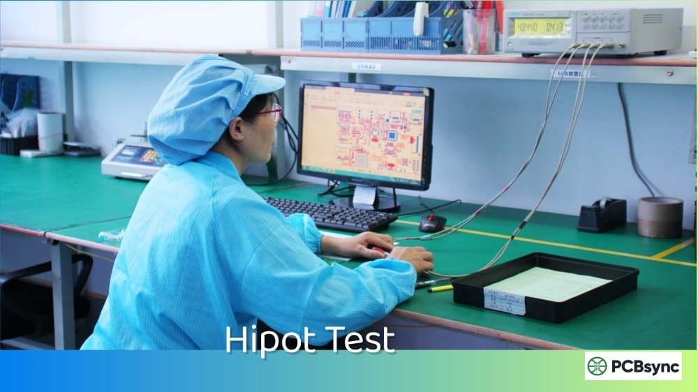
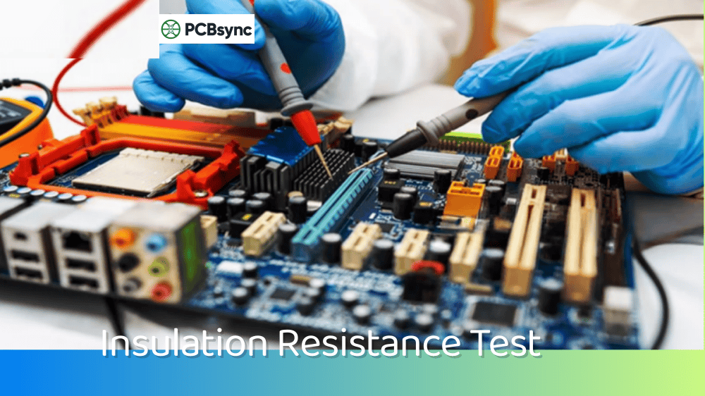
Surface Insulation Resistance (SIR) Testing
SIR testing goes beyond measuring what contaminants are present to understanding their actual impact on electrical performance. This makes it particularly valuable for qualifying no-clean flux processes and high-reliability applications.
How it works: Test boards with standardized comb patterns are placed in a temperature-humidity chamber (typically 85°C/85% RH) under electrical bias. The resistance between conductors is monitored over time (typically 168 to 500 hours). Contamination that causes electrochemical migration will result in decreasing resistance values.
Advantages:
Measures functional impact of contamination
Most relevant test for reliability prediction
Can detect contamination effects ROSE might miss
Essential for no-clean flux process validation
Industry benchmark for process qualification
Limitations:
Long test duration (1-3 weeks)
Specialized equipment and controlled environment required
Not practical for routine production testing
Higher cost per test
SIR Acceptance Criteria: The general requirement is maintaining resistance above 10^8 ohms (100 megohms) throughout the test duration. Some high-reliability specifications require 10^9 ohms or higher.
Localized Ionic Testing (C3 Test)
Traditional ROSE and IC testing extract contaminants from the entire board surface, potentially diluting localized contamination problems. The C3 (Critical Cleanliness Control) test addresses this limitation by focusing extraction on specific critical areas.
When to use localized testing:
Under low-standoff components (QFN, BGA, LGA)
Areas of known flux entrapment
Failure analysis of specific components
High-density interconnect areas
Research shows that localized ionic testing has approximately 76% correlation with SIR testing results, making it a practical intermediate option between ROSE and full SIR qualification.
Contamination Control Best Practices
Testing tells you where you are. Effective contamination control ensures you stay where you need to be. Here are proven strategies I’ve implemented across multiple manufacturing operations.
PCB Fabrication Controls
Immediate post-process rinsing: Don’t let chemical residues sit. Rinsing immediately after plating and etching operations significantly reduces residue adhesion.
DI water in all rinse processes: Municipal water contains ions that can contribute to contamination. Deionized water with resistivity above 10 MΩ·cm should be standard for all final rinse operations.
Final finish selection matters: ENIG (Electroless Nickel Immersion Gold) typically delivers cleaner boards than HASL due to the elimination of aggressive fluxing steps. If HASL is required, ensure thorough post-process cleaning.
Soldermask considerations: Work with your fabricator to select soldermask materials with lower porosity. The pores in soldermask act as contamination reservoirs.
SMT Assembly Controls
Flux selection: Match flux type to your cleanliness requirements. While no-clean flux reduces cleaning steps, it doesn’t eliminate the need for contamination monitoring. Water-soluble flux offers strong cleaning action but requires immediate post-reflow washing.
Flux Type
Cleaning Required
Best Application
Rosin (RMA)
Yes, solvent-based
Hand soldering, rework
Water-soluble
Yes, aqueous
Automated assembly, Class 3
No-clean
Often recommended
High-volume, cost-sensitive
Profile optimization: Proper reflow profiles ensure complete flux activation. Under-heated flux leaves aggressive activators on the board; over-heated flux can bake residues, making them nearly impossible to remove.
Cleaning process validation: If you’re cleaning, validate your process. This means SIR testing during qualification and regular ROSE testing for process control. Target residue levels 50% below your acceptance limit to provide process margin.
Environmental Controls
Humidity management: Maintain assembly and storage areas below 50% relative humidity when practical. Ionic contamination causes problems when moisture is present.
ESD and handling protocols: Human perspiration contains sodium chloride. Use proper ESD gloves and minimize bare-hand contact with board surfaces.
Storage and packaging: Moisture barrier bags with desiccant protect boards from environmental exposure between process steps and during shipping.
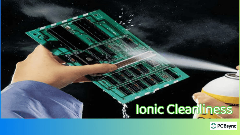
Cleaning Methods for Ionic Contamination Removal
When contamination exceeds acceptable levels, effective cleaning becomes essential.
Aqueous Cleaning
Water-based cleaning systems use heated deionized water, often with saponifiers, to remove flux residues. Typical parameters include:
Water temperature: 55-65°C
Wash time: 3-10 minutes depending on contamination level
Rinse stages: 2-3 minimum
Final rinse resistivity: >10 MΩ·cm
Advantages: Environmentally friendly, effective for water-soluble and many no-clean fluxes, good penetration under components with proper equipment.
Limitations: Moisture sensitivity of some components, requires thorough drying, may not effectively remove all no-clean residues.
Solvent Cleaning
Solvent-based cleaning uses isopropyl alcohol, modified alcohols, or specialized flux removers. Modern formulations balance cleaning effectiveness with environmental and safety concerns.
Best practices:
Match solvent to flux type (consult flux manufacturer recommendations)
Use ultrasonic agitation for stubborn residues
Ensure complete solvent removal and drying
Follow proper ventilation and safety protocols
Ultrasonic Cleaning
Ultrasonic cleaners create microscopic cavitation bubbles that dislodge contaminants from hard-to-reach areas. This method excels at cleaning under low-standoff components where spray systems may not penetrate effectively.
Typical parameters:
Frequency: 40-80 kHz (lower frequencies for robust cleaning, higher for delicate components)
Temperature: 40-60°C
Duration: 3-10 minutes
Caution: Some components, particularly certain ceramic capacitors and crystal oscillators, can be damaged by ultrasonic energy. Verify component compatibility before implementation.
Useful Resources for Further Learning
For those wanting to dive deeper into ionic cleanliness and PCB reliability, here are valuable resources:
Frequently Asked Questions About Ionic Cleanliness
What is the acceptable ionic contamination limit for PCBs?
The traditional industry standard is 1.56 µg NaCl equivalent per cm² (10.06 µg/in²), derived from military specifications dating back over 30 years. However, this limit was established when trace widths and spacings were much larger than today’s designs. For modern high-density boards, many manufacturers and OEMs specify tighter limits between 0.63 and 1.0 µg/cm². High-reliability applications often require limits below 0.5 µg/cm² with ion chromatography verification per IPC-5704.
Can no-clean flux really be left on the board without cleaning?
Despite the name, no-clean flux can still cause reliability issues under certain conditions. The “no-clean” designation means the residues are designed to be benign under normal operating conditions, but problems can arise with high humidity exposure, conformal coating application, or when residues become trapped under low-standoff components. For Class 3 products and any application where conformal coating will be applied, cleaning no-clean flux residues is strongly recommended. Always validate your no-clean process with SIR testing.
How often should ionic cleanliness testing be performed?
For production environments, ROSE testing should be performed at minimum on a per-lot basis for each solder paste lot and any process changes. Many manufacturers test multiple samples per shift. Ion chromatography testing is typically reserved for process qualification, periodic verification (monthly or quarterly), and failure analysis. SIR testing should be performed during initial process qualification and whenever significant process changes occur.
What causes white residue around solder joints?
White residue typically indicates one of several issues: incompletely activated flux that didn’t receive sufficient heat during soldering, flux that was overheated and baked onto the surface, or the formation of metal salts when flux residues react with solder alloys. If you’re seeing white residue, review your reflow profile to ensure flux activation temperatures are reached, and consider whether your cleaning process (if used) is appropriate for your flux type.
How does ionic contamination cause PCB failures?
Ionic contamination causes failures through several mechanisms. First, electrochemical migration (ECM) occurs when ionic residues combine with moisture and electrical bias, causing metal ions to migrate between conductors and form conductive dendrites that create short circuits. Second, corrosion accelerates when ionic residues attract moisture and create localized galvanic cells that attack copper traces and solder joints. Third, parasitic leakage develops as ionic contamination reduces surface insulation resistance, causing current leakage between traces that can disrupt sensitive analog circuits. These failure modes are often intermittent and humidity-dependent, making them particularly challenging to diagnose in the field.
Real-World Case Study: When Ionic Cleanliness Goes Wrong
Let me share a situation I encountered that illustrates why ionic cleanliness matters so much. A manufacturer was experiencing a 3% field failure rate on automotive control modules after about 18 months of service. The failures were intermittent and always occurred during humid summer months.
Initial diagnosis was frustrating because the returned boards passed all electrical tests in the lab. ROSE testing on the failed boards showed contamination levels around 1.4 µg/cm² — technically within the 1.56 µg/cm² spec they had on their fabrication drawing.
Here’s what we discovered: ion chromatography revealed elevated chloride levels concentrated under the BGA controller chip. The bare boards were coming in “clean” by ROSE standards, but the HASL flux was leaving chloride residues trapped in the soldermask pores. Over months of operation in the vehicle’s humid environment, these chlorides were leaching out and causing electrochemical migration between the fine-pitch BGA pads.
The solution involved three changes: switching to ENIG final finish to eliminate the aggressive HASL fluxing, implementing IC testing per IPC-5704 as the acceptance criterion for incoming bare boards, and adding a post-reflow cleaning step with aqueous wash to remove any remaining ionic residues. Field failure rates dropped to under 0.1% within two production quarters.
This case demonstrates why meeting minimum specifications isn’t always enough. The operating environment, component density, and technology level all factor into determining what “clean enough” really means for your specific application.
Conclusion
Ionic cleanliness isn’t just a quality checkbox; it’s a fundamental factor determining whether your PCBs will deliver reliable performance throughout their intended service life. As circuit geometries continue shrinking and reliability expectations keep rising, the margin for error around contamination control continues to narrow.
The good news is that with proper understanding of IPC standards, appropriate testing methods, and disciplined process controls, achieving and maintaining ionic cleanliness is entirely achievable. Start with understanding your specific reliability requirements, implement testing appropriate to those requirements, and establish process controls that keep you well within your limits.
Whether you’re designing boards, selecting suppliers, or managing assembly operations, the investment in ionic cleanliness pays dividends in reduced field failures, lower warranty costs, and products that work reliably in the hands of your customers.
Inquire: Call 0086-755-23203480, or reach out via the form below/your sales contact to discuss our design, manufacturing, and assembly capabilities.
Quote: Email your PCB files to Sales@pcbsync.com (Preferred for large files) or submit online. We will contact you promptly. Please ensure your email is correct.
Notes: For PCB fabrication, we require PCB design file in Gerber RS-274X format (most preferred), *.PCB/DDB (Protel, inform your program version) format or *.BRD (Eagle) format. For PCB assembly, we require PCB design file in above mentioned format, drilling file and BOM. Click to download BOM template To avoid file missing, please include all files into one folder and compress it into .zip or .rar format.


