Inquire: Call 0086-755-23203480, or reach out via the form below/your sales contact to discuss our design, manufacturing, and assembly capabilities.
Quote: Email your PCB files to Sales@pcbsync.com (Preferred for large files) or submit online. We will contact you promptly. Please ensure your email is correct.
Notes: For PCB fabrication, we require PCB design file in Gerber RS-274X format (most preferred), *.PCB/DDB (Protel, inform your program version) format or *.BRD (Eagle) format. For PCB assembly, we require PCB design file in above mentioned format, drilling file and BOM. Click to download BOM template To avoid file missing, please include all files into one folder and compress it into .zip or .rar format.
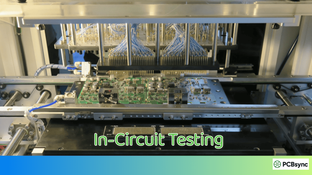
After spending over a decade in PCB manufacturing, I’ve seen countless boards fail in the field because companies skipped proper testing. In-circuit testing remains one of the most reliable methods to catch defects before they become expensive problems. This guide covers everything you need to know about ICT, from basic principles to implementation strategies that actually work on the production floor.
In-circuit testing is an automated testing method that verifies individual components on a populated printed circuit board. Unlike functional testing that checks if the whole board works, ICT isolates each component and measures its electrical characteristics independently.
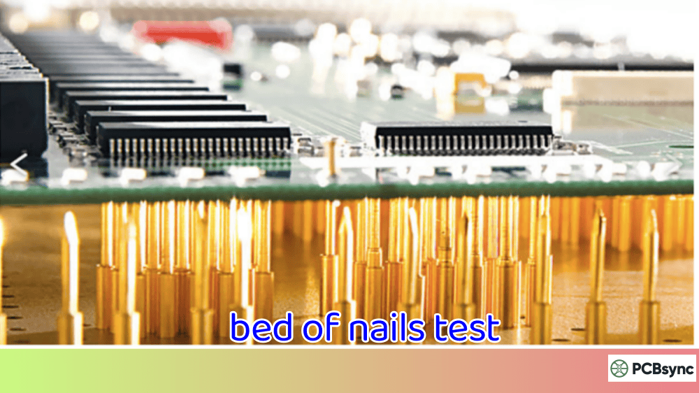
The process uses a bed-of-nails fixture that makes contact with test points on the PCB. Through these contact points, the test system applies signals and measures responses to verify component presence, correct values, and proper orientation.
Think of it like a doctor checking your vital signs before running complex diagnostic tests. ICT confirms the basics are right before moving to more sophisticated testing methods.
How In-Circuit Testing Works
The ICT process follows a straightforward sequence that happens in seconds:
Step 1: Board Loading The PCB is placed on the test fixture, either manually or through automated handling systems.
Step 2: Fixture Engagement The bed-of-nails fixture presses against the board, making electrical contact with designated test points.
Step 3: Component Isolation Using guarding techniques, the tester electrically isolates individual components from surrounding circuitry.
Step 4: Measurement The system applies test signals and measures component responses against programmed limits.
Step 5: Pass/Fail Determination Results are compared to specifications, and the board receives a pass or fail verdict.
Step 6: Data Logging Test results are recorded for quality tracking and statistical process control.
Types of Defects In-Circuit Testing Detects
One of the biggest advantages of in-circuit testing is its ability to catch manufacturing defects that other methods miss. Here’s what ICT reliably detects:
Component-Level Defects
Defect Type
Description
ICT Detection Rate
Missing Components
Parts not placed during assembly
99%+
Wrong Values
Incorrect resistor/capacitor values
98%+
Wrong Orientation
Polarized parts installed backwards
95%+
Wrong Package
Correct value but wrong physical size
90%+
Damaged Components
Parts damaged during handling or soldering
85%+
Solder Joint Defects
Defect Type
Description
ICT Detection Rate
Opens
No electrical connection
99%+
Shorts
Unintended connections between traces
98%+
Insufficient Solder
Weak joints prone to failure
80%+
Solder Bridges
Adjacent pins connected
95%+
PCB Defects
Defect Type
Description
ICT Detection Rate
Trace Opens
Broken copper traces
99%+
Trace Shorts
Shorted traces
98%+
Plating Defects
Via or through-hole issues
85%+
In-Circuit Testing Equipment and Components
Understanding the hardware involved helps you make better decisions about ICT implementation. Here’s what makes up a complete in-circuit testing system:
The ICT System Architecture
Test Controller The brain of the operation. Modern ICT systems use industrial computers running specialized software that controls test sequencing, data acquisition, and result analysis. Major manufacturers include Teradyne, Keysight, and SPEA.
Measurement Instrumentation High-precision instruments measure resistance, capacitance, inductance, voltage, and current. Better systems include programmable power supplies and signal generators for powered testing.
Switching Matrix Routes signals between instrumentation and individual test points. The quality of your switching matrix directly affects measurement accuracy and test speed.
Bed-of-Nails Fixture Custom-built for each PCB design, this fixture holds spring-loaded probes (the “nails”) that contact test points on the board. Fixture quality dramatically impacts test reliability.
Bed-of-Nails Fixture Design
The fixture is where theory meets reality. Poor fixture design causes false failures, missed defects, and production headaches.
Key fixture components include:
Test Probes: Spring-loaded pins that make contact with PCB test points. Common types include spear-point, crown, and serrated tips, each suited for different pad types and surface finishes.
Probe Plates: Hold probes in precise alignment. Usually made from acrylic or phenolic material with tight-tolerance drilled holes.
Wiring Harness: Connects probes to the test system interface. Good harness design minimizes crosstalk and signal degradation.
Mounting Hardware: Aligns the fixture to the tester and provides consistent pressure across all probes.
Choosing the right test strategy means understanding how ICT compares to alternatives. No single method catches everything, so most manufacturers combine approaches.
In-Circuit Testing vs Flying Probe Testing
Factor
In-Circuit Testing
Flying Probe Testing
Test Speed
5-30 seconds per board
1-15 minutes per board
Fixture Cost
$5,000-$50,000+
None (fixtureless)
NRE Cost
High
Low
Best For
High-volume production
Prototypes, low volume
Test Coverage
Excellent
Good
Access Requirements
Many test points needed
Fewer points acceptable
Programming Time
Moderate
Lower
When to choose ICT: High-volume production where fixture cost is justified by throughput gains.
When to choose Flying Probe: Prototypes, low-volume runs, or boards without adequate test points.
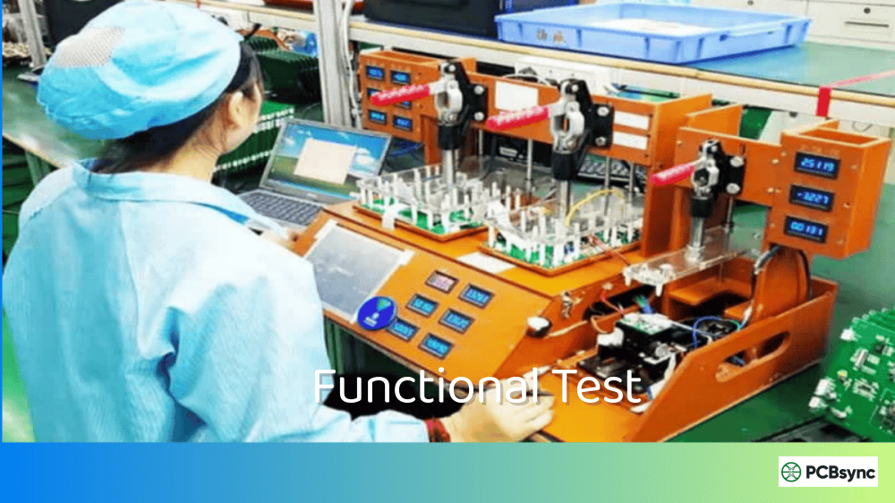
In-Circuit Testing vs Functional Testing
Factor
In-Circuit Testing
Functional Testing
Tests Individual Components
Yes
No
Tests System Function
Limited
Yes
Finds Root Cause
Directly
Requires troubleshooting
Catches Assembly Defects
Excellent
Moderate
Catches Design Defects
No
Yes
Test Development Time
Moderate
High
The practical approach: Use ICT first to verify PCB assembly quality, then functional testing to confirm the design works as intended.
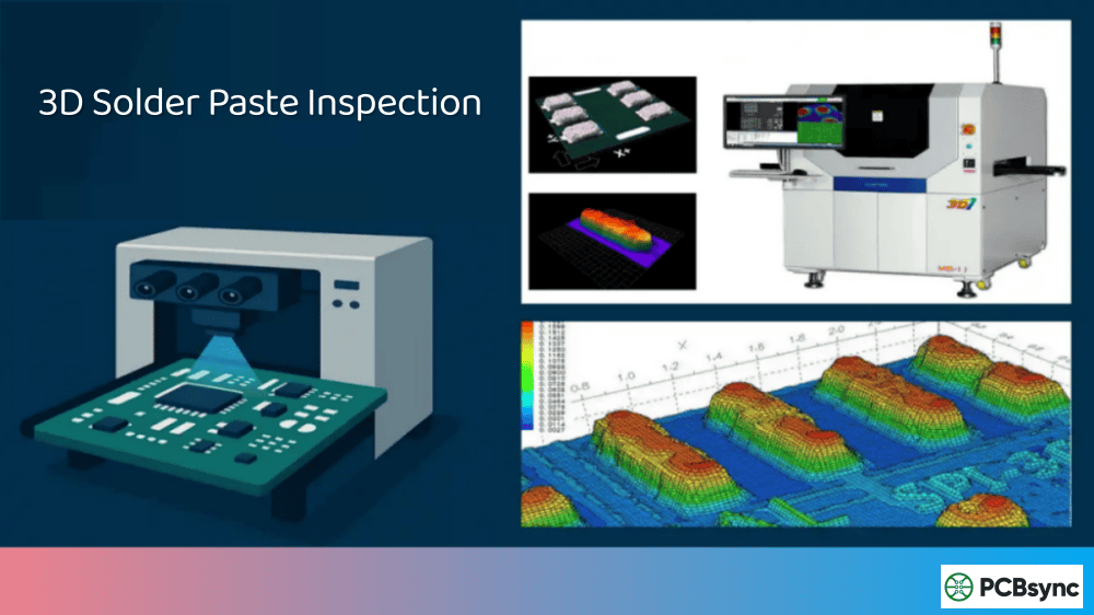
In-Circuit Testing vs Automated Optical Inspection
Factor
In-Circuit Testing
AOI
Detects Wrong Values
Yes
Limited
Detects Solder Shorts
Yes
Yes
Detects Hidden Defects
Yes
No
Verifies Electrical Function
Yes
No
Speed
Moderate
Fast
Setup Cost
High
Moderate
Best practice: AOI catches visual defects quickly and cheaply. ICT catches electrical defects AOI misses. Use both.
Design for In-Circuit Testing (DFT)
Getting maximum value from in-circuit testing starts at the design stage. Boards designed without ICT in mind often become expensive headaches during production.
Test Point Requirements
Test points are the foundation of effective ICT. Every net you want to test needs accessible contact points.
Minimum test point guidelines:
Parameter
Recommended Value
Pad Diameter
0.035″ (0.9mm) minimum
Pad Spacing
0.100″ (2.54mm) minimum
Distance from Components
0.050″ (1.27mm) minimum
Surface Finish
HASL, ENIG, or OSP
Critical nets requiring test points:
Power rails (all voltages)
Ground connections
Clock signals
Reset lines
Communication buses
Analog signal paths
High-current paths
Test Point Placement Strategies
Single-sided probing places all test points on one side of the board, simplifying fixture design and reducing cost. This works well for boards with components on one side only.
Double-sided probing accesses both sides of the board, providing better coverage for complex assemblies but doubling fixture complexity and cost.
Via-in-pad uses component pads as test points when dedicated points aren’t possible. This requires careful probe selection to avoid pad damage.
Common DFT Mistakes to Avoid
Insufficient test point count: Skimping on test points limits fault coverage. Budget for at least 90% net coverage.
Test points too close to components: Probes need clearance. Crowded test points lead to fixture interference and probe damage.
No test points on BGA breakouts: BGA components need test access to verify connections. Add test points on the first via after each BGA pin.
Mixed surface finishes: Different finishes require different probe types. Standardize where possible.
Missing ground test points: Ground plane access is essential for guarding techniques. Include distributed ground test points.
In-Circuit Testing Programming and Development
Turning a PCB design into a working ICT program involves several distinct phases.
Test Program Development Process
Phase 1: Data Import Import CAD data (Gerber files, netlist, BOM) into the ICT development software. Verify data accuracy before proceeding.
Phase 2: Fixture Design Generate fixture drilling files based on test point locations. Consider probe clearances, board support requirements, and handling needs.
Phase 3: Test Generation The ICT software automatically generates basic tests for each component based on the BOM. This covers opens, shorts, and component value verification.
Phase 4: Test Optimization Fine-tune test limits based on component tolerances and measurement capabilities. Tighter limits catch more defects but increase false failures.
Phase 5: Debug and Validation Run the program on known-good boards to verify accuracy. Adjust tests that show marginal results or inconsistent behavior.
Phase 6: Production Release Document the test program and train operators. Establish procedures for handling failures and tracking yield.
Setting Test Limits
Test limits balance defect detection against false failure rates. Too tight causes excessive retesting. Too loose misses real defects.
Recommended limit guidelines:
Component Type
Typical Tolerance
Suggested Test Limit
Resistors (1%)
±1%
±3%
Resistors (5%)
±5%
±10%
Ceramic Capacitors
±20%
±30%
Electrolytic Caps
-20%/+80%
-25%/+100%
Inductors
±10%
±15%
These limits account for component tolerances plus measurement uncertainty. Adjust based on your actual production data.
Advantages of In-Circuit Testing
In-circuit testing delivers measurable benefits that justify the investment for many manufacturers.
Manufacturing Benefits
High Defect Coverage ICT catches 85-95% of manufacturing defects in seconds. No other single method provides comparable coverage at production speeds.
Fast Fault Isolation When ICT finds a defect, it identifies the exact component and failure mode. This eliminates troubleshooting time and gets boards to repair faster.
Reduced Field Failures Boards that pass comprehensive ICT have significantly lower field failure rates. The cost of testing is far less than warranty repairs and customer dissatisfaction.
Process Feedback ICT data reveals process trends before they become yield problems. Tracking component failure rates highlights supplier issues, placement problems, or soldering defects.
Economic Benefits
Factor
Impact
Test Time
10-30 seconds vs minutes for alternatives
Fault Diagnosis
Immediate vs hours of troubleshooting
Throughput
Supports high-volume production
Quality Costs
Catches defects at lowest repair cost point
Limitations of In-Circuit Testing
No test method is perfect. Understanding ICT limitations helps you design appropriate test strategies.
Technical Limitations
Cannot Test Firmware ICT verifies hardware only. Boards need functional testing to confirm programmed devices work correctly.
Limited Dynamic Testing ICT primarily performs DC measurements. High-frequency circuits and timing-sensitive designs need additional verification.
No System-Level Verification ICT confirms components are present and correct but doesn’t verify that the complete system functions as designed.
Access Requirements ICT needs physical test points. High-density boards with limited access may not achieve adequate coverage.
Economic Limitations
Fixture Cost Custom fixtures cost $5,000 to $50,000+ depending on complexity. This investment only makes sense for production volumes that justify the expense.
Setup Time Test program development takes days to weeks. Short product lifecycles may not provide enough production time to recover these costs.
Equipment Investment ICT systems cost $100,000 to $500,000+. Smaller manufacturers may find flying probe or other methods more economical.
In-Circuit Testing Best Practices
These recommendations come from real production experience and help maximize ICT effectiveness.
Fixture Maintenance
Fixtures degrade over time and need regular attention:
Daily: Visual inspection for damaged probes
Weekly: Clean probes with approved solvents
Monthly: Check probe travel and replace worn probes
Quarterly: Verify fixture alignment and update calibration
TestStandards.com: Reference for electronics test methodologies
Advanced In-Circuit Testing Techniques
Modern ICT systems offer capabilities far beyond basic component verification. Understanding these advanced techniques helps you extract maximum value from your testing investment.
Boundary Scan Integration
Boundary scan testing (JTAG) complements traditional ICT by accessing components without physical test points. Modern ICT systems integrate boundary scan capability, allowing test programs to combine both methods.
When to use boundary scan with ICT:
BGA devices where ball connections cannot be probed directly
High-density boards with limited test point real estate
Devices that support IEEE 1149.1 standard
Interconnect testing between boundary-scan compliant devices
The integration works by using ICT probes to access the JTAG port pins while the boundary scan controller handles device communication. This hybrid approach achieves coverage levels impossible with either method alone.
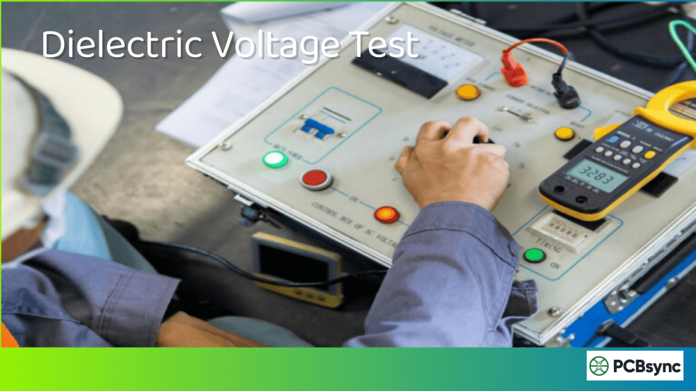
Powered Testing Capabilities
Basic ICT performs unpowered measurements only. Powered testing extends capability by applying operational voltages and observing circuit behavior.
Powered testing applications:
Test Type
What It Verifies
Typical Use Case
Voltage Regulator Output
Correct regulation under load
Power supply circuits
LED Verification
Forward voltage and current
Indicator LEDs
Transistor Function
Gain and switching behavior
Discrete semiconductor circuits
Relay Operation
Coil activation and contact closure
Control circuits
Diode Characteristics
Forward/reverse voltage drops
Protection circuits
Powered testing requires careful limit setting to avoid component stress while still detecting defects. Work with your ICT vendor to develop safe powered test sequences.
Analog Circuit Testing
Analog circuits present unique challenges for in-circuit testing. Component interactions make individual measurements less meaningful, and tolerances stack up unpredictably.
Effective analog ICT strategies:
Subsystem testing: Instead of individual components, measure functional groups like amplifier stages or filter sections as complete units.
Signature analysis: Compare voltage or current signatures against known-good boards rather than absolute specifications.
Parametric guards: Use careful guarding to isolate analog components from surrounding circuitry during measurement.
Multi-point correlation: Measure several related points and look for expected relationships rather than absolute values.
Digital Device Testing
Modern digital devices present their own ICT challenges. The key is understanding what ICT can and cannot verify.
What ICT verifies for digital devices:
Correct device installed (manufacturer ID via JTAG)
Power rail connections present
Clock and reset connections intact
Communication bus connectivity
What ICT cannot verify:
Internal device function
Programmed firmware operation
Full-speed signal integrity
Complex timing relationships
For comprehensive digital device testing, combine ICT with functional test or built-in self-test (BIST) capabilities.
In-Circuit Testing Industry Trends
The ICT landscape continues evolving in response to manufacturing challenges and technological advances.
Miniaturization Challenges
Component sizes continue shrinking while density increases. This creates real problems for traditional ICT:
Shrinking test points: Standard probe pads are becoming impractical on fine-pitch designs. Test engineers now work with 0.5mm or smaller contact areas.
Reduced probe counts: Limited board real estate means fewer test points. This pushes coverage lower unless compensated with other methods.
Higher probe precision: Modern fixtures require tighter tolerance drilling and probe alignment to hit smaller targets consistently.
The industry response includes finer-pitch probe designs, improved fixture manufacturing technology, and greater integration with complementary test methods.
Integration with Industry 4.0
Smart manufacturing demands connected test systems. Modern ICT platforms support:
Real-time data streaming: Test results flow immediately to factory systems for SPC and yield monitoring.
Remote diagnostics: Equipment vendors can troubleshoot systems remotely, reducing downtime.
Predictive maintenance: Systems track probe cycles and predict fixture maintenance needs before failures occur.
Traceability integration: Individual board serial numbers link to complete test records for regulatory compliance.
Combining ICT with Machine Learning
Emerging applications use machine learning to enhance ICT effectiveness:
Adaptive limit setting: Algorithms adjust test limits based on production data, reducing false failures while maintaining defect detection.
Root cause prediction: ML models correlate test failures with upstream process variables to predict defect causes.
Test optimization: Software analyzes test programs and suggests efficiency improvements or coverage gaps.
These capabilities are appearing in newest-generation ICT platforms from major vendors.
Troubleshooting Common In-Circuit Testing Problems
Even well-designed ICT programs encounter issues. Here’s how to address common problems:
High False Failure Rates
False failures waste time and erode confidence in the test process. Common causes include:
Marginal test limits: Limits set too tight for actual component and measurement variation. Solution: Review limit calculations and expand where appropriate.
Inconsistent probe contact: Worn probes, contamination, or fixture misalignment. Solution: Inspect and maintain fixture, verify alignment.
Environmental sensitivity: Temperature or humidity affecting measurements. Solution: Control environment or add compensation.
Intermittent connections: Loose harness wiring or connector issues. Solution: Inspect all connections and repair as needed.
Missed Defects Escaping ICT
When defective boards pass ICT, root cause analysis reveals common issues:
Insufficient coverage: Critical nets lack test points. Solution: Design revision to add access.
Wrong test type: Using resistance test when value test needed. Solution: Review program and add appropriate tests.
Limit too loose: Tolerances allow defective components to pass. Solution: Tighten limits based on actual defect data.
Guarding failures: Adjacent components interfering with measurements. Solution: Review guard configurations and adjust.
Fixture Problems
Fixture issues cause inconsistent results and reduced throughput:
Probe wear: Probes lose spring force or tip condition degrades. Solution: Regular inspection and proactive replacement.
Alignment drift: Fixture loses registration over time. Solution: Verify alignment monthly and adjust as needed.
ICT cost per board depends heavily on volume. For high-volume production with amortized fixture costs, expect $0.10-$0.50 per board. Low-volume runs with dedicated fixtures may cost $2-$10 per board. The key factors are fixture cost, test time, and equipment utilization.
Can in-circuit testing damage PCBs?
When properly configured, ICT is safe for production boards. However, risks exist. Excessive probe pressure can damage test pads or surface finishes. Powered tests with incorrect limits can stress components. Proper fixture design and conservative test parameters minimize these risks.
How long does it take to develop an ICT program?
Simple boards with good DFT take 2-3 days for initial program development. Complex boards with mixed-signal circuitry, tight tolerances, or limited test access may require 1-2 weeks. Debug and validation add additional time depending on board complexity and defect rates.
What test coverage can I expect from in-circuit testing?
Well-designed boards with adequate test points achieve 90-98% fault coverage. Coverage depends on test point availability, component types, and circuit topology. Expect lower coverage for boards with BGA-intensive designs, limited test access, or complex analog circuits.
Should I use in-circuit testing or flying probe testing?
The decision depends primarily on volume. Flying probe makes sense for prototypes and production under 500-1,000 boards annually. ICT becomes economical above this threshold due to faster test times that offset fixture investment. Many manufacturers use flying probe for NPI and transition to ICT for volume production.
Conclusion: Making In-Circuit Testing Work for You
In-circuit testing remains a cornerstone of PCB manufacturing quality despite advances in other inspection methods. The combination of speed, coverage, and diagnostic capability makes ICT essential for medium to high-volume production.
Success with in-circuit testing requires commitment across the product development cycle. Design teams must incorporate testability from the start. Manufacturing engineers need proper fixture design and program development. Quality teams must analyze data and drive continuous improvement.
The investment in in-circuit testing pays dividends through reduced field failures, lower warranty costs, and improved customer satisfaction. For products where quality matters, ICT isn’t optional—it’s essential.
Start your ICT journey by evaluating your current test coverage and identifying gaps. Work with experienced test engineers to develop a strategy that matches your volume, complexity, and quality requirements. The boards you ship will be better for it.
Inquire: Call 0086-755-23203480, or reach out via the form below/your sales contact to discuss our design, manufacturing, and assembly capabilities.
Quote: Email your PCB files to Sales@pcbsync.com (Preferred for large files) or submit online. We will contact you promptly. Please ensure your email is correct.
Notes: For PCB fabrication, we require PCB design file in Gerber RS-274X format (most preferred), *.PCB/DDB (Protel, inform your program version) format or *.BRD (Eagle) format. For PCB assembly, we require PCB design file in above mentioned format, drilling file and BOM. Click to download BOM template To avoid file missing, please include all files into one folder and compress it into .zip or .rar format.


