Inquire: Call 0086-755-23203480, or reach out via the form below/your sales contact to discuss our design, manufacturing, and assembly capabilities.
Quote: Email your PCB files to Sales@pcbsync.com (Preferred for large files) or submit online. We will contact you promptly. Please ensure your email is correct.
Notes: For PCB fabrication, we require PCB design file in Gerber RS-274X format (most preferred), *.PCB/DDB (Protel, inform your program version) format or *.BRD (Eagle) format. For PCB assembly, we require PCB design file in above mentioned format, drilling file and BOM. Click to download BOM template To avoid file missing, please include all files into one folder and compress it into .zip or .rar format.
If you’ve spent any time selecting surface finishes for your PCB projects, you know the decision is never as straightforward as it seems. Each finish comes with trade-offs, and immersion tin PCB is no exception. As someone who has worked through countless board designs and manufacturing runs, I’ve seen immersion tin work brilliantly in some applications and fail miserably in others.
This guide cuts through the marketing fluff and gives you a practical, engineer’s perspective on immersion tin. We’ll cover exactly when this finish makes sense, when you should avoid it, and how to get the best results when you do use it. Whether you’re designing consumer electronics, automotive modules, or high-density interconnect boards, you’ll walk away knowing whether immersion tin belongs in your next project.
Surface finish selection affects everything from solderability and reliability to cost and environmental compliance. With the electronics industry’s ongoing shift toward lead-free manufacturing and increasingly miniaturized components, understanding the nuances of each finish option has become more important than ever. Immersion tin occupies an interesting position in this landscape—offering a compelling balance of cost, performance, and flatness that makes it particularly attractive for specific use cases.
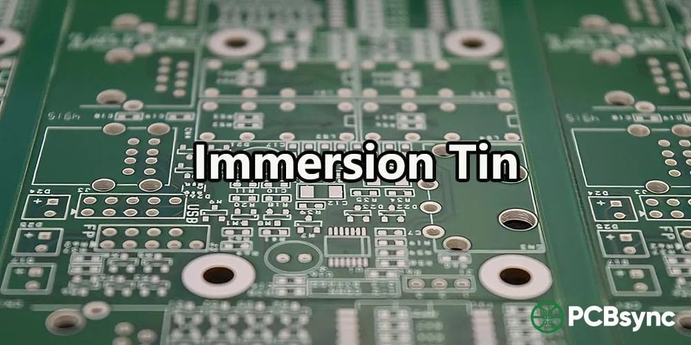
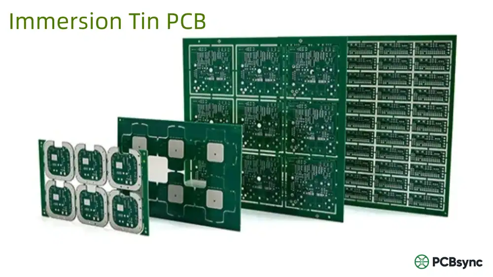
Immersion tin (often abbreviated as ImSn or ISn) is a lead-free surface finish applied to printed circuit boards through an electroless chemical displacement process. Unlike electroplating, which requires external electrical current, immersion tin relies on a simple chemical reaction: tin ions in the plating solution replace copper atoms on the PCB surface, forming a thin, uniform layer of metallic tin.
The result is a matte white or silver-gray coating—which is why you’ll sometimes hear it called “white tin” in the industry. This layer typically ranges from 0.8 to 1.2 micrometers (roughly 32-47 microinches) in thickness, providing protection against copper oxidation while maintaining excellent solderability.
The chemistry behind immersion tin is straightforward but elegant. In the plating bath, tin exists as stannous ions (Sn²⁺) in an acidic solution. When a copper surface is introduced, a displacement reaction occurs: copper atoms give up electrons and dissolve into the solution as Cu²⁺ ions, while tin ions accept those electrons and deposit onto the copper surface as metallic tin. This self-limiting reaction continues until the tin layer becomes thick enough to insulate the underlying copper from the plating solution.
What makes immersion tin particularly useful is that the displacement reaction naturally produces a very flat, uniform coating. The tin deposits evenly regardless of the underlying copper topography, filling into recesses and maintaining consistent thickness across pads, traces, and plated through-holes. This uniformity is critical for modern SMT assembly where component placement precision is measured in microns.
How the Immersion Tin Process Works
The immersion tin plating process follows a sequence of chemical baths that prepare and coat the copper surfaces:
Cleaning and Degreasing: The PCB is immersed in an acid solution to remove oils, grease, and surface contaminants.
Micro-etching: A mild acid treatment removes the oxide layer from copper surfaces and creates micro-roughness for better tin adhesion.
Pre-dip Activation: The board enters an activation bath that prepares the copper surface for the displacement reaction.
Immersion Tin Plating: The PCB is immersed in a heated solution containing stannous chloride (SnCl₂). Tin ions replace copper atoms through electrochemical displacement, depositing a uniform tin layer.
Post-dip and Rinse: Excess tin ions and stabilizers are removed with clean water.
Drying: The board is dried using forced air or a warm oven to remove moisture and prevent staining.
The entire process is governed by IPC-4554, the industry specification for immersion tin plating. This standard defines thickness requirements, solderability testing methods, and quality criteria that ensure consistent results across different manufacturers. Understanding this process helps you evaluate whether your fabricator is following best practices and delivering quality boards.
Process control is critical with immersion tin. Parameters like bath temperature (typically 60-80°C), immersion time, solution pH, and tin ion concentration all affect the final deposit quality. Variations can lead to issues like insufficient thickness, poor adhesion, or uneven coverage. When evaluating fabricators, ask about their process monitoring and quality control procedures—this is where experienced manufacturers differentiate themselves from commodity suppliers.
Let’s be honest about what immersion tin does well. When selected for the right application, it delivers genuine benefits:
Excellent Surface Flatness
This is where immersion tin really shines. The chemical displacement process deposits tin evenly across all copper surfaces, resulting in a coplanar finish with thickness variations of less than 0.1 micrometers. For designs using fine-pitch components (below 0.5mm pitch), BGAs, QFNs, or any surface-mount devices where precise placement matters, this flatness is critical. Unlike HASL, which leaves uneven solder bumps that can cause tombstoning or misalignment, immersion tin provides the smooth, consistent surface that modern SMT assembly demands.
Consider what happens during component placement: a pick-and-place machine positions parts with micron-level accuracy, but if the pad surfaces are uneven, components can tilt, shift during reflow, or fail to make proper contact. With 0201 and 01005 passive components becoming common, and BGA pitches shrinking below 0.4mm, surface planarity isn’t a nice-to-have—it’s essential for achieving acceptable yields. Immersion tin delivers this flatness at a fraction of the cost of ENIG.
Cost-Effective Alternative to ENIG
Budget matters, and immersion tin typically costs 20-30% less than ENIG (Electroless Nickel Immersion Gold). For high-volume consumer electronics or prototyping runs where you need a flat, lead-free finish without the premium price tag of gold, immersion tin hits a sweet spot. The process also uses fewer chemicals and less water than many alternatives, which can translate to lower per-board costs at scale.
When calculating total cost of ownership, factor in the complete picture: board fabrication cost, storage and handling requirements, potential yield impact, and rework expenses. Immersion tin’s lower base cost can be offset if improper handling leads to solderability issues and higher rework rates. However, with proper process controls, the savings are real and meaningful—particularly at volumes where a few cents per board adds up to significant numbers.
Lead-Free and RoHS Compliant
Immersion tin contains no lead, making it fully compliant with RoHS directives and WEEE regulations. If you’re shipping products to the EU or working with environmentally-conscious customers, this isn’t just a nice-to-have—it’s a requirement. The finish works seamlessly with lead-free solder alloys like SAC305 (Sn96.5/Ag3.0/Cu0.5), which is now standard in most manufacturing environments.
Beyond regulatory compliance, immersion tin also offers environmental benefits in pcb manufacturing. The process chemistry is relatively benign compared to some alternatives, and the simpler process (compared to multi-layer finishes like ENIG) means less chemical waste and water usage. For companies with sustainability targets, these factors can be meaningful considerations in the surface finish decision.
Good Initial Solderability
Fresh immersion tin provides excellent wetting characteristics. The tin surface readily accepts solder without the need for aggressive fluxes, making it particularly suitable for wave soldering and reflow processes. For boards that will be assembled within a reasonable timeframe (more on this later), solderability is generally not a concern.
Ideal for Press-Fit Connectors
Here’s something not everyone mentions: immersion tin is the preferred finish for press-fit connector applications. The tin-to-tin interface between the plated through-hole and the connector pin creates a reliable cold-welded connection through the pressing process. This is particularly important in automotive electronics, where press-fit technology has become standard for creating robust, vibration-resistant connections without soldering.
Disadvantages of Immersion Tin PCB Finish
Now for the reality check. Immersion tin has legitimate drawbacks that you need to consider before committing to this finish:
Limited Shelf Life
This is the big one. Immersion tin has a shelf life of approximately 6-12 months under optimal storage conditions—and often less in real-world scenarios. The problem is the copper-tin intermetallic compound (IMC) that forms at the interface between the tin layer and underlying copper. Over time, copper atoms diffuse into the tin layer, eventually reaching the surface and compromising solderability. IPC-4554 specifies a minimum usable tin thickness of 0.4 micrometers (15 µin) if boards are to be soldered within 30 days. Beyond that, you’re gambling with solder joint quality.
The intermetallic formation is a thermodynamic inevitability—copper and tin have a strong affinity for each other, and the driving force for diffusion never stops. Even at room temperature, the Cu-Sn interface is constantly evolving. The practical implication is that you need to plan your supply chain carefully. If your fabricator is shipping boards that then sit in a distributor’s warehouse for three months before reaching your assembly line, you may already be eating into your usable shelf life. For contract manufacturing scenarios with long lead times, this can be a significant constraint.
Tin Whisker Formation Risk
Tin whiskers are microscopic, hair-like crystalline structures that can spontaneously grow from pure tin surfaces. These whiskers can reach lengths of 1-5mm or more, potentially causing short circuits in high-density designs. The growth is driven by compressive stress in the tin layer, often exacerbated by the copper-tin intermetallic formation. While modern immersion tin formulations include additives to inhibit whisker growth (as addressed in JEDEC/IPC JP002 guidelines), the risk never completely disappears. For aerospace, medical, or other high-reliability applications where a single failure could be catastrophic, this is a serious concern.
The tin whisker phenomenon has been documented since the 1940s, and its physics are now well understood. As the copper-tin intermetallic layer grows, it occupies more volume than the original copper atoms, creating compressive stress at the tin surface. This stress is relieved by the spontaneous growth of tin whiskers—essentially, the tin layer is “sweating” out the excess volume. Factors like temperature cycling, humidity, and mechanical stress can accelerate whisker formation. The concern isn’t hypothetical: documented failures in pacemakers, missile systems, and telecommunications equipment have been traced back to tin whiskers.
Sensitive to Handling and Storage
The tin layer is soft and prone to scratching. Even minor abrasions from improper handling can expose the underlying copper, leading to oxidation and localized solderability problems. Fingerprints, contamination from oils, and exposure to humidity all accelerate degradation. This means your manufacturing process needs strict handling protocols: gloves, controlled environments, and protective packaging. It’s not insurmountable, but it adds complexity to your workflow.
Degrades After Multiple Reflow Cycles
Each time an immersion tin board goes through a reflow oven, the tin layer thins as it dissolves into the molten solder. If your assembly process requires multiple reflow cycles (double-sided SMT, for example), the tin may be depleted before the final pass, exposing copper and causing soldering defects. Best practice is to limit reflow cycles to three or fewer, though some manufacturers report issues after just two cycles.
Aggressive to Solder Mask
The acidic chemistry used in immersion tin plating can be aggressive to solder mask materials. This means you need to maintain adequate solder mask dams (typically 5 mil or more) around pads to prevent undercutting or delamination. Not a deal-breaker, but something to factor into your design rules.
Immersion Tin vs. Other Surface Finishes
Understanding how immersion tin stacks up against alternatives helps you make an informed decision. The electronics industry offers several viable surface finishes, each with distinct advantages. ENIG provides superior shelf life and durability but at higher cost. HASL remains the most economical option but fails for fine-pitch designs. OSP offers the lowest cost for flat surfaces but has the shortest shelf life. Immersion silver balances flatness with conductivity but tarnishes easily.
Here’s a practical comparison to help guide your selection:
Factor
Immersion Tin
ENIG
HASL
OSP
Immersion Silver
Cost
Low-Medium
High
Low
Low
Medium
Shelf Life
6-12 months
12+ months
12+ months
3-6 months
6-12 months
Surface Flatness
Excellent
Excellent
Poor
Excellent
Excellent
Solderability
Good
Excellent
Excellent
Good
Good
RoHS Compliant
Yes
Yes
LF only
Yes
Yes
Fine Pitch Suitable
Excellent
Excellent
Poor
Excellent
Excellent
Tin Whisker Risk
Yes
No
Minimal
No
No
Press-Fit Suitable
Excellent
Good
Poor
Good
Good
Thickness
0.8-1.2 µm
3-6 µm Ni, 0.05-0.1 µm Au
1-25 µm
0.2-0.5 µm
0.1-0.4 µm
When to Use Immersion Tin PCB Finish
Based on its strengths and limitations, immersion tin makes sense in these scenarios:
Ideal Applications
Immersion tin finds its sweet spot in applications that leverage its flatness and cost advantages while avoiding its shelf life limitations:
Fine-Pitch SMT Components: Designs using 0201 resistors, micro-BGAs, QFNs, or components with pitch below 0.5mm benefit from the exceptional flatness.
Press-Fit Connector Applications: Automotive ECUs, power distribution modules, and telecom backplanes using compliant-pin connectors perform well with immersion tin.
High-Volume Consumer Electronics: Smartphones, tablets, IoT devices, and other products with short production-to-assembly cycles and cost sensitivity.
Prototyping and Development: When boards will be assembled within weeks of fabrication and budget matters.
HDI (High-Density Interconnect) Boards: The uniform plating coverage works well with via-in-pad designs and tight geometries.
When to Avoid Immersion Tin
Knowing when NOT to use immersion tin is equally important. Avoid this finish in these scenarios:
Aerospace and Military Applications: The tin whisker risk and limited shelf life make ENIG or other finishes a safer choice.
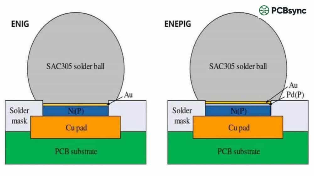
Medical Devices (Class II/III): Long-term reliability requirements typically call for ENIG or ENEPIG.
Long Inventory Cycles: If boards might sit in storage for 6+ months before assembly, choose a finish with longer shelf life.
Multiple Reflow Processes: Boards requiring 3+ reflow cycles may experience tin depletion issues.
Wire Bonding Applications: ENIG or ENEPIG are better suited for gold or aluminum wire bonding.
IPC-4554 Specification Requirements
IPC-4554 is the governing specification for immersion tin plating on printed circuit boards. Understanding its key requirements helps ensure you’re getting quality boards from your fabricator:
The specification was developed by IPC’s Plating Subcommittee (4-14) and amended in 2011 to address solderability testing with both tin-lead and lead-free solder alloys. It establishes a framework for consistent quality across the industry, covering everything from visual inspection criteria to thickness measurement protocols. When evaluating potential fabricators, asking whether they follow IPC-4554 and how they verify compliance is a reasonable quality gate.
Key parameters defined in IPC-4554:
Parameter
Requirement
Total Tin Thickness
1.0-1.2 µm (40-47 µin) typical range
Minimum Usable Tin
0.4 µm (15 µin) for soldering within 30 days
Shelf Life Category
J-STD-003 Category 3 (>6 months storage)
Solderability Testing
Wetting balance test per J-STD-003
Visual Appearance
Matte white to light gray, uniform coverage
The distinction between “total tin thickness” and “usable tin thickness” is important. As copper diffuses into the tin layer, it forms an intermetallic compound that’s no longer pure tin—and doesn’t solder as well. XRF measurements typically show total tin thickness, but what matters for solderability is the remaining pure tin layer. This is why IPC-4554 emphasizes the usable tin minimum rather than just total thickness.
Storage and Handling Best Practices
Getting the most out of immersion tin requires attention to storage and handling. Proper care can extend usable shelf life significantly and prevent costly solderability issues during assembly. Here’s what works based on industry best practices and IPC-1601A guidelines:
Control Storage Environment: Maintain temperature between 15-25°C (59-77°F) and relative humidity below 50%. Avoid temperature fluctuations that cause condensation.
Use Moisture Barrier Bags (MBBs): Store boards in vacuum-sealed MBBs with desiccant packets and humidity indicator cards. This can extend usable life by up to 50%.
Handle with Gloves: Always use lint-free ESD gloves. Oils from bare hands accelerate oxidation and can cause solderability issues.
Implement FIFO Inventory: First-in, first-out inventory management ensures older boards are used before their shelf life expires.
Minimize Air Exposure: Once boards are removed from packaging, assemble them within 24-48 hours if possible.
Avoid Baking Before Use: Unlike some finishes, pre-baking immersion tin boards can actually accelerate intermetallic compound formation and degrade solderability.
Test Solderability: For boards approaching 6 months in storage, conduct solderability testing before committing to a production run.
Troubleshooting Common Immersion Tin Issues
Even with proper storage and handling, issues can arise. Here’s how to diagnose and address common problems:
Dewetting During Soldering: If solder beads up or retracts from pads during reflow, the most likely cause is oxidation of the tin surface. This can result from extended storage, exposure to humidity, or contamination. Solutions include verifying storage conditions, using a more active flux, or if the boards are marginal, applying a thin flux coat before assembly.
Non-Wetting: When solder fails to wet the pad at all, the tin layer may be depleted or excessively oxidized. Check the board manufacturing date and storage history. If the boards are within their shelf life but still showing non-wetting, the plating thickness may have been insufficient—work with your fabricator to investigate.
Surface Discoloration: Immersion tin should appear matte white to light gray. Yellowing or dark spots indicate oxidation or contamination. Minor discoloration doesn’t necessarily mean the boards are unusable—conduct solderability testing to verify. Severe discoloration typically indicates storage issues.
Inconsistent Solder Joint Quality: If some joints are good while others show defects, investigate both the board condition and your assembly process. Verify reflow profile temperatures, flux coverage, and stencil condition. Sometimes the root cause is actually in the assembly process rather than the board finish.
Frequently Asked Questions
What is the shelf life of immersion tin PCB?
Under optimal storage conditions (temperature 15-25°C, humidity <50%, in sealed moisture barrier bags), immersion tin PCBs have a shelf life of 6-12 months. However, in typical warehouse conditions without climate control, effective shelf life may be closer to 3-6 months. The IPC-4554 specification classifies immersion tin as a Category 3 finish per J-STD-003, meaning it should maintain solderability for greater than 6 months under proper storage. If boards have been stored for extended periods, conduct solderability testing before assembly.
Is immersion tin RoHS compliant?
Yes, immersion tin is fully RoHS compliant. It contains no lead, cadmium, mercury, or other restricted substances. The finish was developed specifically as a lead-free alternative to traditional HASL (Hot Air Solder Leveling) and is compatible with lead-free soldering processes using SAC alloys. This makes it suitable for products sold in the EU and other regions with environmental regulations.
Can immersion tin withstand multiple reflow cycles?
Immersion tin can typically withstand 2-3 reflow cycles, but performance degrades with each pass. During reflow, the tin layer dissolves into the molten solder, thinning the protective coating. After three reflows, the remaining tin may be insufficient to protect the copper, leading to oxidation and solderability issues. If your assembly process requires multiple reflows (such as double-sided SMT), plan the process sequence carefully and consider testing solderability after each reflow stage.
How does immersion tin compare to ENIG for fine-pitch components?
Both immersion tin and ENIG provide excellent surface flatness suitable for fine-pitch components. The key differences are: ENIG offers longer shelf life (12+ months vs. 6-12 months for immersion tin), better corrosion resistance, and no tin whisker risk. However, ENIG costs 20-30% more and has the potential for “black pad” defects if the plating process isn’t well-controlled. For cost-sensitive projects with short production cycles, immersion tin is a solid choice. For high-reliability applications or long inventory cycles, ENIG is the safer option.
What causes tin whiskers and how can I prevent them?
Tin whiskers are crystalline filaments that grow spontaneously from pure tin surfaces due to compressive stress in the tin layer. The primary stress source is copper-tin intermetallic compound formation at the interface, which creates volume changes that drive whisker nucleation. To minimize whisker risk: use modern immersion tin formulations with whisker-inhibiting additives (look for processes compliant with JEDEC JESD201), assemble boards promptly rather than storing for extended periods, consider applying conformal coating after assembly as a barrier against whisker bridging, and design with adequate trace spacing (above 0.3mm) to reduce the likelihood of shorts.
Useful Industry Resources
For engineers who want to dive deeper, these resources provide authoritative information on immersion tin and PCB surface finishes:
IPC-4554: Specification for Immersion Tin Plating for Printed Circuit Boards – The definitive industry standard. Available from IPC Shop
JEDEC JESD201: Environmental Acceptance Requirements for Tin Whisker Susceptibility – Testing and acceptance criteria for tin whisker risk. Available from JEDEC
JEDEC/IPC JP002: Current Tin Whiskers Theory and Mitigation Practices Guideline – Comprehensive guidance on understanding and mitigating tin whisker formation.
J-STD-003: Solderability Tests for Printed Boards – Testing methods for evaluating surface finish solderability.
IPC-1601A: Printed Board Handling and Storage Guidelines – Best practices for PCB storage and handling to maximize shelf life.
NASA Tin Whisker Homepage: Extensive research database on tin whisker failures and mitigation – nepp.nasa.gov/whisker
iNEMI Tin Whisker Resources: Industry consortium research on tin whisker testing and mitigation – inemi.org
Final Thoughts
Immersion tin isn’t a perfect surface finish—but then again, no finish is. It delivers genuine value for the right applications: excellent flatness for fine-pitch components, reliable press-fit performance, RoHS compliance, and reasonable cost. The key is understanding its limitations and planning accordingly.
If your production cycle is short, your boards will be assembled within a few months of fabrication, and you’re working with cost-sensitive consumer electronics or press-fit connectors, immersion tin is a solid choice. If you’re designing for aerospace, medical devices, or applications requiring extended storage or multiple reflow cycles, look at alternatives like ENIG or ENEPIG.
The best surface finish is always the one that matches your specific requirements—not the cheapest or the most expensive, but the one that balances cost, manufacturability, and reliability for your application. Use the comparison tables and guidelines in this article to make an informed decision, and don’t hesitate to consult with your PCB fabricator about their specific immersion tin process and capabilities.
Remember that surface finish selection is just one piece of the overall design puzzle. Work closely with your fabricator and assembly partner to ensure your entire manufacturing process—from design rules to storage protocols to reflow profiles—is optimized for the finish you choose. A well-executed immersion tin process, combined with proper handling and timely assembly, can deliver excellent results at a competitive cost. The knowledge you’ve gained here puts you in a strong position to make that happen.
For complex or high-volume projects, consider running a small pilot build with immersion tin boards before committing to full production. Test solderability, inspect for defects, and verify that your assembly process achieves acceptable yields. This upfront investment in validation can save significant headaches—and costs—down the line.
Inquire: Call 0086-755-23203480, or reach out via the form below/your sales contact to discuss our design, manufacturing, and assembly capabilities.
Quote: Email your PCB files to Sales@pcbsync.com (Preferred for large files) or submit online. We will contact you promptly. Please ensure your email is correct.
Notes: For PCB fabrication, we require PCB design file in Gerber RS-274X format (most preferred), *.PCB/DDB (Protel, inform your program version) format or *.BRD (Eagle) format. For PCB assembly, we require PCB design file in above mentioned format, drilling file and BOM. Click to download BOM template To avoid file missing, please include all files into one folder and compress it into .zip or .rar format.


