Inquire: Call 0086-755-23203480, or reach out via the form below/your sales contact to discuss our design, manufacturing, and assembly capabilities.
Quote: Email your PCB files to Sales@pcbsync.com (Preferred for large files) or submit online. We will contact you promptly. Please ensure your email is correct.
Notes: For PCB fabrication, we require PCB design file in Gerber RS-274X format (most preferred), *.PCB/DDB (Protel, inform your program version) format or *.BRD (Eagle) format. For PCB assembly, we require PCB design file in above mentioned format, drilling file and BOM. Click to download BOM template To avoid file missing, please include all files into one folder and compress it into .zip or .rar format.
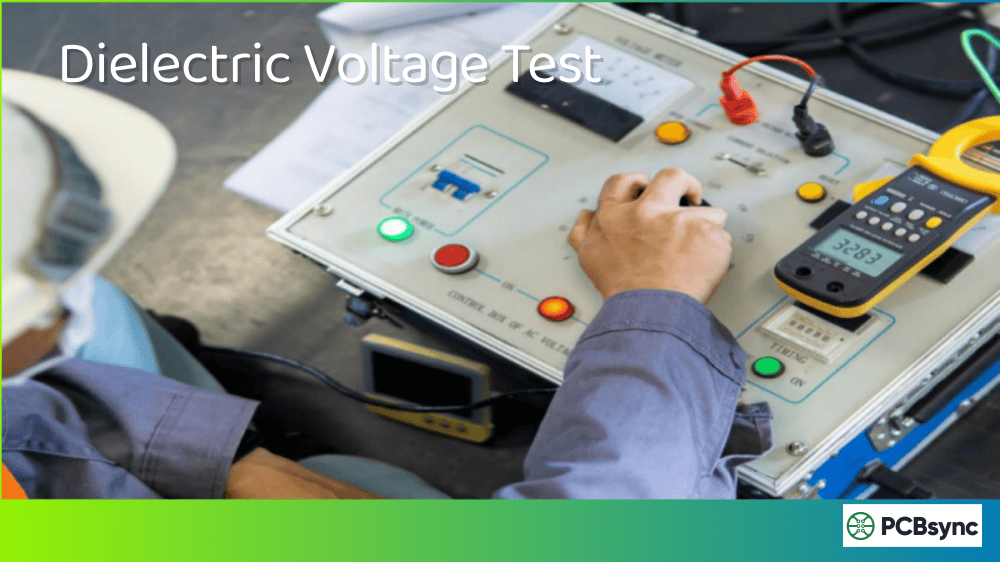
After 15 years of working in PCB manufacturing, I can tell you that few tests are as critical—and as misunderstood—as the Hipot test. Whether you’re a design engineer specifying test requirements or a quality manager trying to reduce field failures, understanding High Potential (Hipot) testing is essential for producing reliable, safe electronics.
In this guide, I’ll walk you through everything you need to know about Hipot testing in PCB manufacturing and SMT assembly, from the basic principles to advanced troubleshooting techniques I’ve learned on the factory floor.
What is a Hipot Test?
A Hipot test, short for High Potential test, is a non-destructive electrical safety test that verifies the insulation integrity of a PCB by applying a voltage significantly higher than its normal operating voltage. Also known as the Dielectric Withstand Voltage test, this procedure determines whether your board’s insulation can handle voltage stress without breaking down.
Think of it this way: if your PCB is designed to operate at 12V, we need to know it won’t fail when voltage spikes occur during normal use. The Hipot test stresses the insulation beyond typical conditions to catch potential failures before they reach your customers.
According to IPC-TM-650, the Hipot test specifically examines the insulation between power and ground layers in a PCB. The test proves that a printed board can operate safely at its rated voltage and withstand momentary voltage spikes due to switching, surges, and similar phenomena.
Why Hipot Testing Matters in PCB Manufacturing
Every PCB engineer has heard horror stories about field failures. I’ve seen products recalled because of insulation breakdown that could have been caught with proper Hipot testing. Here’s why this test is non-negotiable:
Safety Compliance: Most international safety standards including IEC 60950, UL, and CSA require Hipot testing for product certification. Without passing this test, your product simply cannot enter many markets.
Early Defect Detection: A Hipot test catches manufacturing defects that other tests miss. Problems like insufficient clearance between traces, contamination on the PCB surface, pinholes in insulation, and poor quality dielectric material all show up during Hipot testing.
Cost Savings: Finding insulation problems at the factory is infinitely cheaper than dealing with field failures, recalls, and liability issues. I’ve calculated that catching a defect during Hipot testing costs roughly 1/100th of addressing the same defect after product shipment.
Customer Confidence: When you can demonstrate that every board passes Hipot testing, you’re providing documented proof of quality. This matters enormously in medical, aerospace, and automotive applications.
Types of Hipot Tests for PCB Applications
Understanding the different Hipot test categories helps you select the right approach for your application.
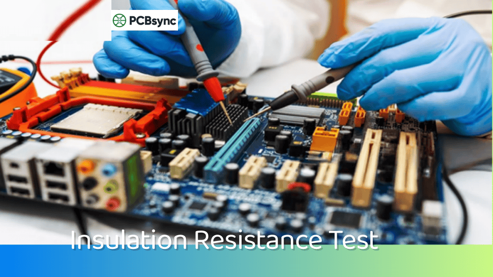
Insulation Resistance Test
This test measures the resistance value of the insulation between traces. By applying a known voltage and measuring the resulting current, we calculate the insulation resistance. A good PCB should show resistance in the megohm or gigohm range.
Dielectric Withstanding Test
The standard Hipot test applies a high voltage for a specified duration while monitoring for breakdown. The PCB passes if the insulation holds without excessive leakage current or arcing. This is the most common production test.
Dielectric Breakdown Test
Unlike the withstanding test, the breakdown test is destructive. Engineers gradually increase voltage until the insulation fails, determining the actual breakdown voltage. This test is typically used for material qualification rather than production testing.
IPC Standards for Hipot Testing
The IPC has established clear guidelines for Hipot testing through IPC-TM-650. Understanding these standards is crucial for setting up your test properly.
Test Conditions According to IPC-TM-650
Parameter
Condition A
Condition B
Test Voltage
500V DC
1000V DC
Ramp Rate
1 second per 100V
1 second per 100V
Dwell Time
30 seconds (+3/-0 sec)
30 seconds (+3/-0 sec)
Current Threshold
Per specification
Per specification
Key Standards Reference Table
Standard
Application
Key Requirements
IPC-TM-650
PCB Testing Methods
Defines Hipot test procedures for bare boards
IPC-6012
Rigid PCB Qualification
Performance specifications including dielectric
IPC-9252A
Electrical Testing
Guidelines for electrical test requirements
IPC-2221
PCB Design Standard
Spacing and clearance requirements
IEC 60950
IT Equipment Safety
3kVAC input-to-output isolation
IEC 60601
Medical Equipment
4kVAC for medical applications
How to Calculate Hipot Test Voltage
Determining the correct test voltage is critical. Too low, and you might miss defects. Too high, and you risk damaging good boards.
Standard Formula:
Hipot Test Voltage = (2 × Working Voltage) + 1000V
For example, if your PCB operates at 220V AC:
Test Voltage = (2 × 220) + 1000 = 1440V
Standard practice rounds this to 1500V AC
DC Equivalent Calculation:
When using DC instead of AC for Hipot testing:
DC Test Voltage = AC Test Voltage × 1.414
For a 1500V AC test, the equivalent DC voltage would be:
DC Voltage = 1500 × 1.414 = 2121V DC
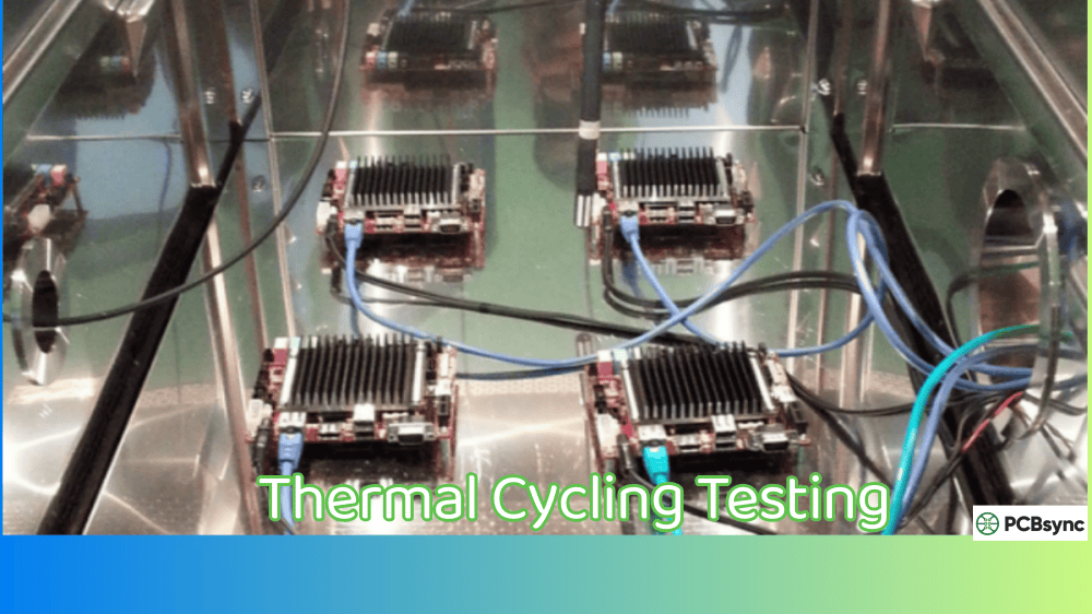
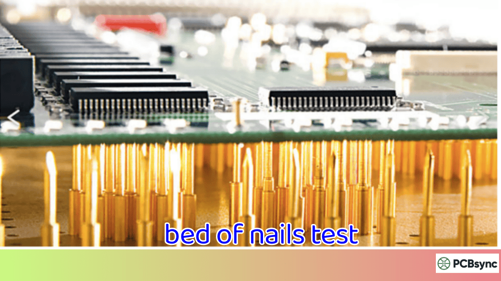
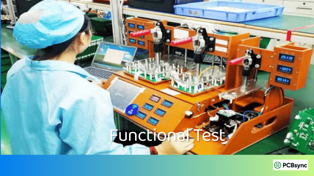
Read more about PCBSync electronic testing method:
This is one of the most common questions I get from engineers setting up new production lines. Both methods have their place.
AC Hipot Test Advantages
The AC Hipot test applies an alternating voltage at line frequency (50 or 60 Hz), which closely simulates real-world operating conditions for AC-powered equipment.
Pros:
Tests both polarities simultaneously
More readily accepted by safety agencies
No discharge required after testing
Better simulation of actual operating conditions
No voltage ramp-up needed
Cons:
Can trigger false failures on high-capacitance circuits
Higher output current required
Cannot easily distinguish real from capacitive current
DC Hipot Test Advantages
DC testing applies a constant unidirectional voltage, making it particularly useful for certain applications.
Pros:
More accurate leakage current measurement
Lower output power requirements
Better at detecting pinholes and voids
Works well with high-capacitance loads
Detects surface contamination effectively
Cons:
Tests only one polarity
Requires proper voltage ramping
Must discharge DUT after testing
Higher voltage levels needed
AC vs. DC Hipot Comparison Table
Factor
AC Hipot
DC Hipot
Voltage Type
Sinusoidal 50/60 Hz
Constant DC
Test Voltage (typical)
1500V AC
2121V DC
Polarity Testing
Both simultaneously
Single polarity
Leakage Measurement
Total current (resistive + capacitive)
True leakage only
Discharge Required
No
Yes
Capacitive Load Handling
May show false failures
Handles well
Regulatory Acceptance
Preferred
Acceptable with voltage factor
Equipment Cost
Generally lower
Slightly higher
Hipot Test Procedure: Step-by-Step Guide
Having set up dozens of Hipot test stations, here’s the procedure I recommend:
Pre-Test Preparation
Step 1: Verify that the PCB is a fresh specimen. Never perform Hipot testing on boards that have already been exposed to high voltage levels or similar testing.
Step 2: Check environmental conditions. For qualification testing, condition specimens at 23°C ± 3°C and 50% ± 10% relative humidity for 24 hours.
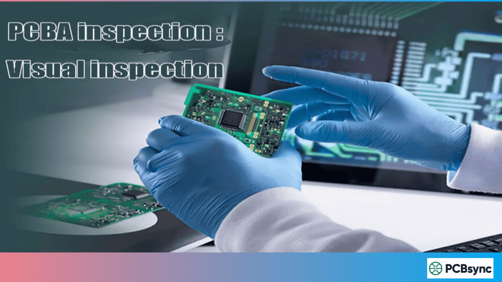
Step 3: Visually inspect the board for obvious defects. There’s no point running electrical tests on a board with visible contamination or damage.
Step 4: Configure the Hipot tester with appropriate parameters:
Peak voltage per specification
Voltage ramp rate (typically 5% of peak voltage per second)
Hold time (30 seconds for qualification, minimum 10 seconds for conformance)
Current threshold level
Test Execution
Step 5: Connect the test probes to the appropriate test points. For power/ground isolation testing, connect one probe to the power net and the other to the ground net.
Step 6: Initiate the test sequence. The tester will:
Ramp voltage from zero to the specified peak
Hold at peak voltage for the specified duration
Monitor leakage current throughout
Automatically discharge the specimen (critical for DC testing)
Step 7: Record the results including test voltage, leakage current, and pass/fail status.
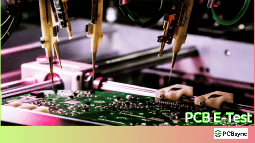
Test Methods Comparison
Method
Equipment
Operator Involvement
Best For
Manual Probing
Hipot analyzer + probes
High (moves probes between pairs)
Prototypes, low volume
Fixture Testing
Analyzer + custom fixture
Medium (places board, initiates test)
Medium volume production
Flying Probe
Automated flying probe machine
Low (fully automated)
High volume, multiple test pairs
Common Hipot Test Failures and Root Causes
After investigating hundreds of Hipot failures, I’ve identified the most common causes:
Manufacturing Defects
Resin Voids: Air pockets in the laminate reduce insulation strength. These often occur during lamination when air gets trapped between layers.
Resin Starvation: Insufficient resin in the fiberglass weave creates weak points. This is especially problematic in high-density designs.
Incomplete Etching: Residual copper between traces reduces clearance and provides a path for arcing. Look for signs of underetching in your process.
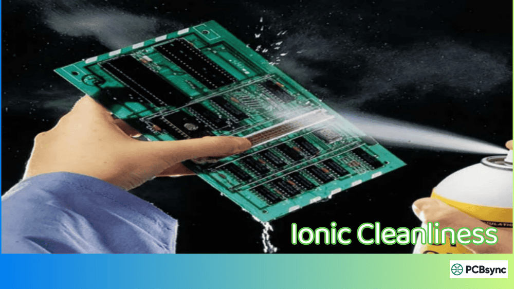
Ionic Contamination: Residual flux, fingerprints, or processing chemicals create surface leakage paths. This is one of the most common causes I encounter.
Design Issues
Insufficient Clearance: The spacing between power and ground planes or between traces and the board edge may not meet requirements for the test voltage.
Material Selection: Some dielectric materials have lower breakdown voltages than others. High-Tg materials often perform differently than standard FR-4.
Via Proximity: Vias too close to plane edges can create weak points in the insulation.
Failure Analysis Decision Tree
Symptom
Likely Cause
Investigation Method
Immediate breakdown
Short circuit, insufficient clearance
Cross-section analysis
Gradual current increase
Contamination, moisture
Cleaning, baking, retest
Intermittent failures
Marginal clearance, particle contamination
Microscopy, SEM
Arcing at surface
Surface contamination, conformal coat issues
Visual inspection, ion chromatography
High leakage, no breakdown
Bulk material degradation, moisture absorption
Material testing, TGA
Hipot Testing Equipment and Setup
Selecting the right equipment significantly affects test reliability and throughput.
Essential Equipment Specifications
Your Hipot tester should provide:
Adjustable output voltage (0-6kV AC and/or 0-6kV DC minimum)
Programmable ramp rates
Adjustable current trip settings (typically 0.5 mA to 20 mA)
Automatic discharge function
Data logging capability
Test Fixture Considerations
For production testing, a well-designed fixture dramatically improves throughput and repeatability:
Use properly insulated probe contacts rated for your test voltage
Include interlocks to prevent operation with an open fixture
Design for easy loading and unloading
Consider automated switching for multiple test pairs
What is the difference between Hipot test and insulation resistance test?
The Hipot test (dielectric withstand) verifies that insulation won’t break down at high voltage, while the insulation resistance test measures the actual resistance value of the insulation at a lower voltage. Think of Hipot as a go/no-go test for breakdown, while insulation resistance provides a quantitative measurement. Both tests complement each other—a board could have acceptable insulation resistance but still fail Hipot due to localized weak spots.
How long should a Hipot test last?
According to IPC-TM-650, qualification testing requires a 30-second dwell time at peak voltage. For production conformance testing, the minimum is 10 seconds, though most safety standards specify 60 seconds as the full test duration. Many manufacturers use accelerated testing at 1-2 seconds with a 20% voltage increase for high-volume production. The key is consistency—whatever duration you choose, maintain it across all units.
Can Hipot testing damage my PCB?
When performed correctly with appropriate voltage levels and duration, Hipot testing is non-destructive. However, improper testing can damage insulation. Never exceed specified voltage levels, avoid repeated testing of failed units, and ensure proper discharge after DC testing. Some degradation of marginal insulation can occur, which is actually the point—we want to find those weak boards before they reach customers.
What causes a PCB to fail Hipot test?
The most common causes are contamination (flux residue, fingerprints, ionic contamination), insufficient trace spacing, material defects (voids, delamination, resin starvation), moisture absorption, and design issues (inadequate clearances for the intended application). When investigating failures, start with visual inspection and cleaning before assuming a fundamental design or material problem.
Do all PCBs need Hipot testing?
Not all applications require Hipot testing, but any product where insulation failure could cause safety hazards should undergo this test. Medical devices, power supplies, industrial equipment, and products requiring safety certification absolutely need Hipot testing. Even for consumer electronics, Hipot testing provides valuable quality assurance. The cost of testing is minimal compared to the cost of field failures.
Conclusion
Hipot testing remains one of the most effective tools for ensuring PCB reliability and safety. By understanding the principles, following proper procedures, and selecting appropriate test parameters, you can catch insulation defects before they become field failures.
Remember these key points:
Use the formula (2 × Working Voltage) + 1000V as your starting point for test voltage
Choose AC testing for regulatory compliance and DC testing for sensitive leakage measurements
Follow IPC-TM-650 guidelines for test parameters
Never skip safety precautions when working with high voltage
Investigate failures systematically rather than simply retesting
Whether you’re setting up a new production line or optimizing an existing process, proper Hipot testing is an investment in product quality that pays dividends through reduced returns, fewer warranty claims, and enhanced customer confidence.
If you have questions about implementing Hipot testing in your facility or need help troubleshooting specific issues, drop a comment below. I’ve learned a lot from the challenges other engineers have faced, and I’m always happy to share what I know.
Inquire: Call 0086-755-23203480, or reach out via the form below/your sales contact to discuss our design, manufacturing, and assembly capabilities.
Quote: Email your PCB files to Sales@pcbsync.com (Preferred for large files) or submit online. We will contact you promptly. Please ensure your email is correct.
Notes: For PCB fabrication, we require PCB design file in Gerber RS-274X format (most preferred), *.PCB/DDB (Protel, inform your program version) format or *.BRD (Eagle) format. For PCB assembly, we require PCB design file in above mentioned format, drilling file and BOM. Click to download BOM template To avoid file missing, please include all files into one folder and compress it into .zip or .rar format.


