Inquire: Call 0086-755-23203480, or reach out via the form below/your sales contact to discuss our design, manufacturing, and assembly capabilities.
Quote: Email your PCB files to Sales@pcbsync.com (Preferred for large files) or submit online. We will contact you promptly. Please ensure your email is correct.
Notes: For PCB fabrication, we require PCB design file in Gerber RS-274X format (most preferred), *.PCB/DDB (Protel, inform your program version) format or *.BRD (Eagle) format. For PCB assembly, we require PCB design file in above mentioned format, drilling file and BOM. Click to download BOM template To avoid file missing, please include all files into one folder and compress it into .zip or .rar format.
If you’ve ever had a prototype come back from fab and wondered why your 100 MHz clock looks like a drunk sine wave on the oscilloscope, welcome to high-speed PCB design. I’ve been laying out boards for over fifteen years, and I still remember the first time I realized that my traces weren’t just wires—they were transmission lines with opinions about how signals should travel.
High-speed PCB design isn’t magic, though it can feel that way when you’re debugging your first signal integrity nightmare at 2 AM. It’s physics, and once you understand the fundamental rules, you can design boards that work the first time. This guide covers everything from deciding when your design actually qualifies as “high-speed” to advanced routing techniques that will keep your signals clean and your EMI emissions under control.
Whether you’re working on USB 3.0, DDR4 memory interfaces, Ethernet, or PCIe, the principles remain the same. Let’s break them down.
The good news? You don’t need to be a PhD-level electromagnetics expert to design reliable high-speed boards. You need to understand a handful of core concepts, apply them consistently, and know when to reach for simulation tools. This guide gives you that foundation, with practical tips drawn from real-world design experience.
Here’s something that trips up a lot of engineers: high-speed design isn’t defined by clock frequency alone. A 50 MHz signal with a 1 ns rise time can cause more problems than a 500 MHz signal with a slow edge rate. The real question is whether your PCB’s physical characteristics start affecting signal quality.
The classic rule of thumb comes from looking at rise time relative to trace length. When a signal’s edge rate is fast enough that the trace length exceeds about one-tenth of the signal wavelength, that trace stops behaving like a simple wire and starts acting like a transmission line. At that point, you’re officially in high-speed territory.
For practical purposes, most signals above 50 MHz with fast edge rates require high-speed design consideration. Anything in the multi-gigabit range—think USB 3.0 at 5 Gbps, HDMI 2.0 at 6 Gbps per channel, or 10 Gigabit Ethernet—absolutely demands it.
When Does a Design Become High-Speed?
Signal Characteristic
Threshold for High-Speed Consideration
Rise/Fall Time
Below 1 ns
Signal Frequency
Above 50 MHz
Data Rate
Above 100 Mbps
Trace Length
Longer than λ/10 of signal wavelength
Edge Rate × Trace Length
When propagation delay exceeds 20% of rise time
The calculation is straightforward. Signal speed in FR4 is approximately 6 inches per nanosecond (15 cm/ns). For a signal with a 1 ns rise time, the critical length is about 0.6 inches (1.5 cm). Beyond that length, you need to treat the trace as a transmission line.
Key Signal Integrity Issues in High-Speed Design
Understanding the problems you’re trying to prevent helps you make better design decisions. Here are the primary signal integrity issues that plague high-speed boards:
Reflections: When a signal encounters an impedance discontinuity (a change in trace width, a via, a connector), part of the energy reflects back toward the source. These reflections superimpose on the original signal, causing ringing, overshoot, and undershoot. In severe cases, reflections cause false triggering of logic gates or corrupt data.
Crosstalk: Adjacent traces couple through their electromagnetic fields. The aggressor trace induces noise on the victim trace, which can be mistaken for valid signal transitions. Near-end crosstalk (NEXT) appears at the transmitter end; far-end crosstalk (FEXT) appears at the receiver end.
Attenuation (Loss): As signals travel along a trace, they lose energy to the dielectric material (dielectric loss) and to the copper itself (conductor loss). This attenuation closes the eye diagram and reduces noise margins. Attenuation increases with frequency and trace length.
Jitter: Timing variations in signal edges caused by noise, power supply fluctuations, or crosstalk. Jitter eats into timing margins and can cause bit errors in high-speed serial links.
Ground Bounce: When multiple outputs switch simultaneously, the transient current through package and PCB inductance causes the local ground potential to shift momentarily. This affects signal levels and can cause false triggering.
Why High-Speed PCB Design Matters
Every time I hear someone say “it’s just a prototype, I’ll fix the layout later,” I cringe. Poor high-speed design creates problems that can’t be fixed in software:
Signal Integrity Degradation: Impedance mismatches cause reflections that corrupt data. I’ve seen USB devices fail certification because of 15% impedance variations that seemed “close enough” during design.
Electromagnetic Interference (EMI): Fast edges radiate. A board that works fine on the bench can fail EMC testing spectacularly because return currents took unexpected paths.
Timing Failures: Skew between differential pairs or clock-data relationships can push you outside timing margins, causing intermittent failures that are nearly impossible to debug.
Power Integrity Issues: High-speed switching demands clean power. Poor PDN design causes ground bounce and simultaneous switching noise (SSN) that shows up as jitter on your signals.
The cost of getting it wrong is measured in re-spins, delayed schedules, and late nights with an oscilloscope. The cost of getting it right upfront is just some extra planning time.
15 Expert Tips for High-Speed PCB Design
Tip 1: Start with Proper Stackup Design
The stackup is the foundation of every high-speed board. Get it wrong, and you’re fighting uphill battles with impedance control, crosstalk, and EMI for the entire project.
For most high-speed designs, a 4-layer board is the minimum. The classic configuration places signal layers adjacent to ground planes:
Recommended 4-Layer Stackup:
Layer 1: Signal (Top)
Layer 2: Ground Plane
Layer 3: Power Plane
Layer 4: Signal (Bottom)
This arrangement gives your high-speed traces on Layer 1 a solid ground reference immediately below them. The tight coupling to ground controls impedance and provides a low-inductance return path.
For more complex designs, 6-layer and 8-layer stackups offer additional routing layers with dedicated planes:
6-Layer High-Speed Stackup:
Layer 1: Signal
Layer 2: Ground
Layer 3: Signal
Layer 4: Power
Layer 5: Ground
Layer 6: Signal
The key principle is always having a solid reference plane adjacent to every signal layer carrying high-speed traces. Never route high-speed signals on layers sandwiched between two signal layers—the impedance becomes unpredictable.
Stackup Design Checklist:
Every high-speed signal layer has an adjacent plane layer
Ground planes are as continuous as possible (no splits under high-speed signals)
Power and ground plane pairs are placed close together for maximum capacitance
The stackup is symmetric about the center (prevents warping during fabrication)
Prepreg and core thicknesses are chosen to achieve target impedance
Tip 2: Control Your Impedance
Impedance control is non-negotiable for high-speed design. The target impedance depends on your signaling standard:
Interface
Single-Ended Impedance
Differential Impedance
USB 2.0/3.0
45Ω
90Ω
HDMI
50Ω
100Ω
PCIe
50Ω
85Ω
Ethernet
50Ω
100Ω
DDR4
40-60Ω
80-120Ω
SATA
50Ω
100Ω
Impedance is determined by trace width, spacing (for differential pairs), dielectric thickness, and the dielectric constant (Dk) of your PCB material. Use your PCB fab’s impedance calculator or a tool like Saturn PCB Toolkit to determine trace widths before you start routing.
A typical impedance tolerance is ±10%. For demanding applications, you might need ±5%, but be prepared to pay more—tighter tolerances require more process control during fabrication.
Always specify impedance requirements in your fabrication notes. Include target impedances, tolerances, and reference layers. Request test coupons if you need verification.
Tip 3: Use a Solid Ground Plane
I cannot stress this enough: never split your ground plane under high-speed signals. The return current for any signal flows directly beneath the trace on the reference plane. If you force that current to detour around a split, you’ve created a loop antenna.
The ground plane should be:
Continuous under all high-speed routing
Dedicated to a single layer when possible
Connected with multiple vias to other ground regions
Free of cuts, slots, or routing on the plane layer
If you absolutely must cross a split in the ground plane (for example, separating analog and digital sections), place the crossing at a single-point connection and ensure it’s not in the path of any high-speed return currents.
Tip 4: Apply the 3W Rule for Trace Spacing
Crosstalk between adjacent traces is one of the most common high-speed problems. The 3W rule provides a conservative guideline: maintain spacing between trace centers of at least three times the trace width.
For a 5-mil trace, that means 15 mils center-to-center spacing (or 10 mils edge-to-edge). This reduces crosstalk by approximately 70%.
In dense routing areas, you may need to violate this rule briefly. If so:
Minimize the parallel run length
Increase spacing again as soon as possible
Use guard traces grounded with vias for critical signals
Remember that crosstalk happens vertically too. If you route signals on adjacent layers directly over each other (broadside coupling), you’ll get crosstalk. Route orthogonally between layers—if Layer 3 runs horizontal, route Layer 4 vertical.
Tip 5: Route Differential Pairs Correctly
Differential signaling is the backbone of high-speed interfaces like USB, HDMI, Ethernet, and PCIe. The technique offers excellent noise immunity because both traces experience the same interference, which cancels out at the differential receiver.
To get these benefits, you must maintain symmetry:
Differential Pair Routing Rules:
Keep both traces the same length (typical tolerance: ±5 mils within a pair)
Maintain consistent spacing throughout the route
Use the same number of vias on both traces
Place vias symmetrically when changing layers
Never route anything between the traces
Match impedance to the protocol specification
Length matching is critical because skew between the positive and negative signals appears as common-mode noise. For a 10 Gbps signal, even a 1 mm mismatch can cause timing problems.
When length tuning is needed, use gentle serpentine patterns with smooth curves rather than sharp corners. Keep the serpentine amplitude small (under 3x trace width) to minimize impedance discontinuities.
Protocol-Specific Differential Pair Requirements:
Protocol
Diff. Impedance
Max Skew
Max Length Mismatch
Notes
USB 2.0
90Ω ±10%
N/A
50 mils
Less critical
USB 3.0/3.1
90Ω ±10%
100 ps
10 mils
Tight matching required
HDMI 1.4/2.0
100Ω ±10%
200 ps
20 mils
Per channel matching
PCIe Gen3
85Ω ±15%
5 ps/inch
5 mils
Very tight matching
PCIe Gen4/5
85Ω ±10%
5 ps/inch
3 mils
Simulation recommended
DDR4
80-100Ω
2.5 ps
Per IC datasheet
Address/command to clock
Ethernet 1G
100Ω ±10%
N/A
100 mils
More tolerant
10G Ethernet
100Ω ±10%
50 ps
20 mils
Tighter requirements
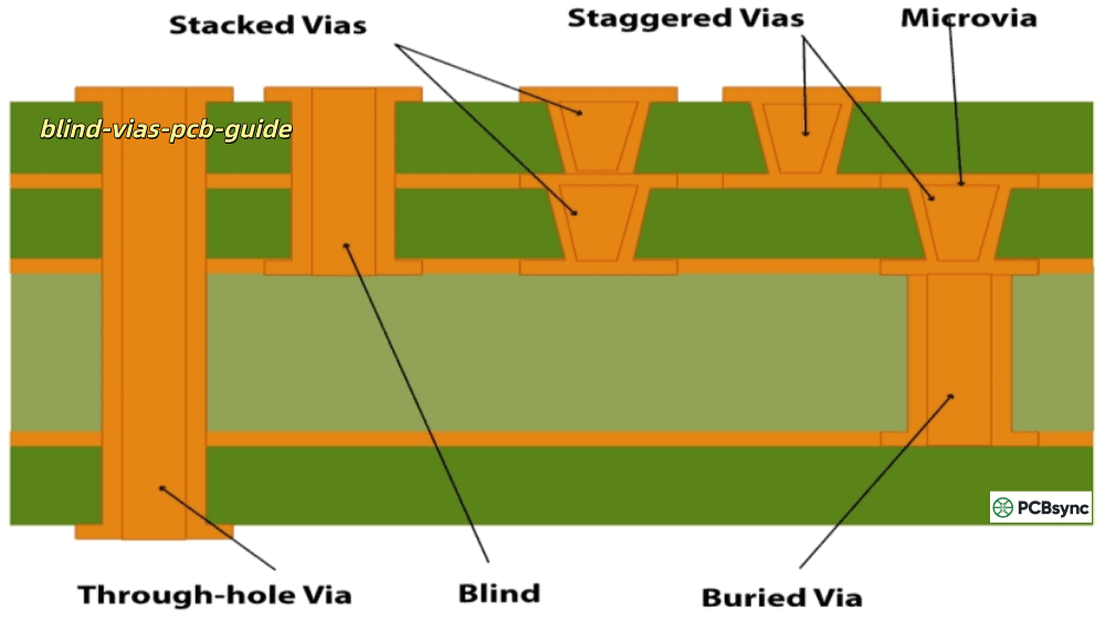
Tip 6: Minimize Via Stubs
Every via has a stub—the unused portion of the barrel that extends past the signal layer. At high frequencies, this stub acts as an antenna and causes reflections.
For signals above 3 Gbps, via stubs become a significant source of signal degradation. Solutions include:
Back-drilling: The fab house drills out the unused stub after plating. This is the most common solution for high-speed designs and adds minimal cost.
Blind/Buried Vias: These vias only connect the layers you need, eliminating stubs entirely. More expensive but necessary for very high-speed designs.
Via-in-Pad: Placing vias directly in component pads eliminates the stub and pad-to-via trace. Essential for fine-pitch BGAs and high-speed escape routing.
The rule of thumb: keep stub length shorter than one-quarter of the switching speed’s equivalent wavelength. For 10 Gbps signals, that means stubs under about 10 mils.
Every signal has a return current, and that current wants to flow directly beneath the signal trace. High-frequency return currents take the path of least impedance, not least resistance.
Design implications:
Don’t route high-speed signals over plane splits
Place ground vias near signal vias when changing layers
If a signal transitions from one reference plane to another, place stitching capacitors or ground vias nearby
Keep decoupling capacitors between the power and ground planes close to the ICs
When a signal changes layers and the reference plane changes (say, from ground to power), the return current needs a path between those planes. Without stitching capacitors, the current takes a longer path, increasing inductance and creating EMI.
Tip 8: Use Proper Termination
Termination matches the transmission line impedance to prevent reflections. The right strategy depends on your circuit topology:
Series Termination: A resistor at the source (typically 22-33Ω) combines with the driver’s output impedance to match the trace impedance. Works well for point-to-point connections and consumes no DC power.
Parallel Termination: A resistor to ground or a voltage reference at the receiver end. Absorbs reflections but draws constant current. Common in bus architectures.
AC Termination (RC): A capacitor in series with the termination resistor blocks DC current while providing AC termination. Good for CMOS outputs that need to reach rail voltages.
Differential Termination: A resistor between the positive and negative traces at the receiver, matching the differential impedance (typically 100Ω).
Many modern ICs include on-die termination (ODT), which eliminates the need for external resistors. Always check the datasheet—adding external termination when ODT is enabled causes over-termination and signal degradation.
Termination Strategy Selection Guide:
Topology
Best Termination
Typical Values
Considerations
Point-to-point
Series at source
22-33Ω
No DC power consumption
Bus with multiple loads
Parallel at end
50-100Ω to GND
Draws DC current
Long trace lengths
Series + Parallel
Varies
May need both
Differential pairs
100Ω between traces
100Ω at receiver
Most protocols use this
LVDS
Parallel differential
100Ω
Usually near receiver
High-speed memory (DDR)
On-die termination
Enabled in IC
Check datasheet
Tip 9: Select the Right PCB Materials
Standard FR4 works fine for many designs, but has limitations at higher frequencies. The dielectric constant (Dk) varies with frequency and the loss tangent (Df) increases signal attenuation.
Material
Dk
Df
Best For
Standard FR4
4.2-4.8
0.020-0.025
Up to 1 GHz, cost-sensitive
High-Speed FR4 (Isola 370HR)
4.0-4.2
0.015-0.018
Up to 3 GHz
Rogers RO4003C
3.38
0.0027
RF up to 10+ GHz
Rogers RO4350B
3.48
0.0037
RF/Microwave
Megtron 6
3.4
0.002
High-speed digital, server
For most digital designs up to a few GHz, standard or high-speed FR4 is sufficient. The cost difference to premium materials is significant (5-10x), so don’t specify Rogers unless you actually need it.
The decision factors:
Signal frequency and data rate
Trace length (longer traces = more loss)
Impedance tolerance requirements
Cost constraints
A hybrid approach works well: use Rogers or Megtron for the high-frequency signal layers and FR4 for power/ground planes and low-speed signals.
Popular High-Speed PCB Material Series:
Material Family
Typical Applications
Key Features
Isola 370HR
General high-speed digital
Enhanced FR4, good thermal performance
Isola I-Tera MT40
Server, telecom
Very low loss, stable Dk
Panasonic Megtron 6
High-speed digital, networking
Low loss, good for 25+ Gbps
Rogers RO4000 series
RF, microwave, automotive radar
Low Dk, FR4-compatible processing
Rogers RO3000 series
Satellite, 5G antennas
Ultra-low loss, ceramic-filled
Nelco N4000-13
Aerospace, military
High reliability, low loss
Taconic TLY
High-frequency RF
PTFE-based, very low loss
Material Selection Decision Tree:
Is your highest signal frequency below 1 GHz? → Standard FR4 is likely fine
Between 1-5 GHz with moderate trace lengths? → High-speed FR4 variants
Above 5 GHz or very long traces? → Consider Rogers/Megtron
RF/microwave application? → Rogers or PTFE-based materials
Cost-sensitive but need some improvement? → Hybrid stackup
Tip 10: Avoid Common Routing Mistakes
After reviewing hundreds of designs, I see the same mistakes repeatedly:
90° Corners: Sharp corners cause impedance discontinuities and reflections. Use 45° mitered corners or smooth arcs instead.
Routing Near Board Edges: Traces within 10-15 mils of the board edge see impedance changes because the reference plane ends. Keep high-speed signals away from edges.
Trace Width Changes: Abrupt width changes create reflections. When you must change width (like escaping from a BGA), taper gradually.
Long Parallel Runs: Two signals running parallel for extended distances couple heavily. Minimize parallel length and maximize spacing.
Crossing Plane Gaps: Return currents can’t cross gaps in the reference plane. If you must cross, provide a low-impedance path with stitching capacitors or vias.
Tip 11: Place Components Strategically
Good placement solves half your routing problems before you draw a single trace.
High-Speed IC Placement:
Place connected high-speed components close together to minimize trace length
Align components so differential pairs can route directly between them
Keep clock sources close to their loads
Position bypass capacitors as close to power pins as physically possible
Termination Placement:
Series termination resistors go at the source, right next to the driver
Parallel termination goes at the receiver
Keep termination components on the same layer as the signal when possible
Decoupling Strategy:
Place bulk capacitors (10-100 µF) near power entry
Place medium capacitors (0.1-1 µF) near each IC
Place small capacitors (10-100 nF) directly at power pins
Use multiple values in parallel to cover a wider frequency range
Tip 12: Design Your Power Distribution Network (PDN)
High-speed signals demand clean power. Every time an output switches, it draws current from the power distribution network. If the PDN can’t supply that current fast enough, the voltage droops, causing jitter and timing problems.
PDN Design Principles:
Target impedance should be low enough that worst-case current draw causes acceptable voltage ripple (typically <5%)
Place power and ground planes adjacent to each other for maximum plane capacitance
Use multiple decoupling capacitor values to cover different frequency ranges
Minimize the inductance of capacitor mounting (short, wide traces or via-in-pad)
The PDN impedance curve should stay flat across the frequency range of your switching signals. Simulation tools like Sigrity or HyperLynx can analyze PDN performance before fabrication.
Tip 13: Manage EMI from the Start
EMI problems discovered during compliance testing are expensive to fix. Design for EMC from the beginning:
Emission Reduction:
Use the slowest edge rates that meet timing requirements
Keep high-speed signals on inner layers sandwiched between planes
Minimize loop areas in signal and return paths
Shield sensitive traces with ground pours (connected with vias)
Susceptibility Reduction:
Filter power supply inputs
Use differential signaling where possible
Add guard traces around sensitive analog signals
Include ferrite beads on I/O lines if needed
Edge Rate Control: Many ICs offer programmable slew rate control. Slower edges radiate less but have tighter timing margins. Find the balance that meets both EMC and timing requirements.
EMI Design Guidelines Summary:
Problem
Prevention Strategy
Radiated emissions from traces
Use stripline routing on inner layers
Common-mode radiation
Ensure balanced differential pairs
Clock harmonics
Add spread-spectrum clocking if supported
Power supply noise
Proper decoupling and PDN design
ESD susceptibility
Add TVS diodes on I/O lines
Conducted emissions
Filter power inputs with common-mode chokes
Ground bounce
Reduce loop inductance, multiple ground pins
Tip 14: Verify with Simulation
For complex high-speed designs, simulation catches problems before you spend money on prototypes.
Pre-Layout Simulation:
Verify stackup impedance with your fab’s calculator
Analyze PDN impedance with target current profiles
Check timing budgets with estimated trace lengths
Post-Layout Simulation:
Extract actual trace lengths and impedances
Run signal integrity simulation (eye diagrams, TDR)
Verify crosstalk between adjacent nets
Analyze return path discontinuities
Tools like HyperLynx, Sigrity, and ADS are industry standards. For simpler checks, Altium Designer and Cadence Allegro include built-in signal integrity analysis.
Tip 15: Work with Your Fab House Early
Your PCB manufacturer is a critical partner for high-speed design. Engage them early to:
Verify Stackup Feasibility:
Confirm material availability
Get actual Dk values for impedance calculation
Understand their process tolerances
Optimize for Manufacturability:
Review minimum trace/space for your impedance targets
Discuss via capabilities (aspect ratio, back-drilling)
Confirm registration tolerances for layer alignment
Control Impedance:
Specify impedance targets and tolerances clearly
Request impedance test coupons
Review their impedance control process
A quick design review with your fab can prevent expensive surprises. Most reputable manufacturers offer free DFM checks that catch issues before production.
High-Speed PCB Design Process: Step by Step
A structured approach prevents the most common high-speed design failures. Here’s the process that works:
Step 1: Requirements Analysis
Before opening your CAD tool, define the high-speed requirements:
List all high-speed interfaces and their specifications
Identify impedance targets and tolerances
Determine layer count and board size constraints
Establish the material requirements based on frequencies involved
Review IC datasheets for layout guidelines
Step 2: Stackup Design
Work with your fabricator to define:
Number of layers and arrangement
Material selection for each layer
Dielectric thicknesses for impedance targets
Copper weights for current handling
Overall board thickness
Step 3: Component Placement
Critical placement decisions:
High-speed components close together to minimize trace length
Bypass capacitors immediately adjacent to power pins
Sensitive analog circuits separated from digital noise sources
Connectors positioned for clean signal escape
Test points accessible without disrupting signal paths
Step 4: Fanout and Initial Routing
Start with the most constrained signals:
BGA escape routing
Differential pair planning
Critical timing groups (clocks, memory buses)
Power delivery paths
Step 5: High-Speed Routing
Apply all the techniques discussed:
Controlled impedance routing
Length matching
Crosstalk prevention
Via management
Termination placement
Step 6: Verification
Before releasing to fabrication:
Design rule check (DRC)
Impedance verification
Length matching check
Signal integrity simulation (if warranted)
Power integrity analysis
Manufacturing review (DFM)
High-Speed PCB Design Software and Tools
Effective high-speed design requires the right tools. Here’s what the industry uses:
EDA (Electronic Design Automation) Software
Tool
Strengths
Best For
Altium Designer
Integrated SI analysis, good constraint management
Routing high-speed signals near board edges: Impedance goes unpredictable.
Using the wrong termination strategy: Over-termination wastes power; under-termination causes reflections.
Neglecting power integrity: Clean signals require clean power.
Not simulating before fabrication: Much cheaper to catch problems in software.
Specifying materials without checking availability: Exotic laminates have long lead times.
Forgetting to request controlled impedance: Your fab won’t control what you don’t specify.
Routing clock signals as an afterthought: Clocks are often the highest-frequency signals on the board.
Frequently Asked Questions (FAQs)
What defines a high-speed PCB design?
A PCB design becomes “high-speed” when the physical characteristics of the board—trace length, geometry, and material properties—start affecting signal quality. The practical threshold is when trace length exceeds about one-tenth of the signal wavelength, or when rise/fall times are below 1 nanosecond. Most digital interfaces operating above 50 MHz with fast edge rates require high-speed design techniques including controlled impedance, proper stackup design, and attention to return paths.
Can I use standard FR4 material for high-speed PCB design?
Yes, for many applications. Standard FR4 works well for digital signals up to about 1-2 GHz and moderate trace lengths. The limitations appear with longer traces, higher frequencies, or tight impedance tolerances due to FR4’s variable dielectric constant and higher loss tangent. For signals above 3 GHz or very long traces, consider high-speed FR4 variants (like Isola 370HR) or premium materials like Rogers or Megtron. The extra cost of specialty materials only makes sense when standard FR4 genuinely can’t meet your performance requirements.
How many layers do I need for high-speed PCB design?
At minimum, four layers. A 4-layer board provides dedicated ground and power planes with two signal layers—enough for simpler high-speed designs. More complex designs with high pin-count BGAs, multiple high-speed interfaces, or dense routing typically require 6, 8, or more layers. The key principle is ensuring every high-speed signal layer has an adjacent solid reference plane. A 2-layer board cannot reliably support controlled impedance routing because there’s no reference plane beneath the traces.
What is the difference between microstrip and stripline routing?
Microstrip traces are on the outer layers of the PCB, with a reference plane below. Stripline traces are on inner layers, sandwiched between two reference planes. Stripline offers better EMI shielding because the signal is enclosed by ground planes, making it ideal for the most sensitive high-speed signals. Microstrip is easier to probe and test but radiates more. For best performance, route critical high-speed signals (especially differential pairs and clocks) as stripline on inner layers, using microstrip for component connections and less critical signals.
How do I reduce crosstalk in high-speed PCB designs?
Several strategies work together to minimize crosstalk. First, increase spacing between traces—the 3W rule (center-to-center spacing of three times trace width) reduces crosstalk by about 70%. Second, route signals over a solid ground plane close to the traces; smaller distance to ground means tighter field containment. Third, minimize parallel run length between aggressor and victim traces. Fourth, route orthogonally between layers (horizontal on one layer, vertical on the next). Finally, for critical signals, use guard traces connected to ground with vias to provide additional isolation.
Conclusion
High-speed PCB design is fundamentally about managing the physics of signal propagation. Once you accept that your traces are transmission lines and your return currents need low-impedance paths, the design rules make intuitive sense.
Start with a solid stackup, control your impedance, respect your ground planes, and simulate before you fabricate. These fundamentals apply whether you’re designing a USB hub or a 100 Gbps backplane.
The field keeps advancing—data rates double every few years, and design margins shrink. But the underlying principles haven’t changed much since transmission line theory was developed decades ago. Master the fundamentals, and you’ll adapt to whatever new interfaces and speeds come next.
Good luck with your next high-speed design. May your eye diagrams be open and your EMI scans be clean.
Author Note: This guide reflects practical experience from designing high-speed boards across consumer electronics, telecommunications, and industrial applications. The recommendations are based on industry best practices, IC manufacturer guidelines, and lessons learned from both successful designs and debugging sessions. Always verify specifications against current component datasheets and interface standards for your specific application.
Inquire: Call 0086-755-23203480, or reach out via the form below/your sales contact to discuss our design, manufacturing, and assembly capabilities.
Quote: Email your PCB files to Sales@pcbsync.com (Preferred for large files) or submit online. We will contact you promptly. Please ensure your email is correct.
Notes: For PCB fabrication, we require PCB design file in Gerber RS-274X format (most preferred), *.PCB/DDB (Protel, inform your program version) format or *.BRD (Eagle) format. For PCB assembly, we require PCB design file in above mentioned format, drilling file and BOM. Click to download BOM template To avoid file missing, please include all files into one folder and compress it into .zip or .rar format.


