Inquire: Call 0086-755-23203480, or reach out via the form below/your sales contact to discuss our design, manufacturing, and assembly capabilities.
Quote: Email your PCB files to Sales@pcbsync.com (Preferred for large files) or submit online. We will contact you promptly. Please ensure your email is correct.
Notes: For PCB fabrication, we require PCB design file in Gerber RS-274X format (most preferred), *.PCB/DDB (Protel, inform your program version) format or *.BRD (Eagle) format. For PCB assembly, we require PCB design file in above mentioned format, drilling file and BOM. Click to download BOM template To avoid file missing, please include all files into one folder and compress it into .zip or .rar format.
What is High Frequency PCB? Materials, Design Guidelines & Best Practices
Introduction
High Frequency PCB technology has become the backbone of modern telecommunications, aerospace, and advanced electronics. As 5G networks expand globally and devices demand faster signal transmission, understanding high frequency printed circuit boards is no longer optional—it’s essential for engineers and designers working with cutting-edge technology.
A High Frequency PCB is a specialized printed circuit board engineered to operate at frequencies above 1 GHz with minimal signal loss and exceptional signal integrity. Unlike standard PCBs that struggle with high-speed signals, these advanced boards use specialized materials and precise design techniques to maintain clean signal transmission at microwave and radio frequencies.
The global market for high frequency PCBs is projected to exceed $3.5 billion by 2025, driven by explosive growth in 5G infrastructure, automotive radar systems, and IoT devices. Whether you’re designing a satellite communication system or developing next-generation wireless technology, mastering high frequency PCB design is crucial for success.
In this comprehensive guide, we’ll explore what makes high frequency PCBs unique, compare critical materials, outline essential design guidelines, and share proven best practices that ensure your designs perform flawlessly.
A High Frequency PCB is a printed circuit board specifically designed to handle electromagnetic signals operating at frequencies typically above 500 MHz, with most applications focusing on the 1 GHz and higher range. These specialized boards are engineered to transmit signals in the microwave and radio frequency spectrum with minimal loss and distortion.
The industry generally categorizes PCB frequencies as follows:
High Frequency: 500 MHz to 3 GHz
Microwave Frequency: 3 GHz to 30 GHz
Millimeter Wave (mmWave): 30 GHz to 100 GHz and beyond
At these elevated frequencies, standard PCB materials like FR4 experience significant signal degradation due to high dielectric losses. This is where specialized high frequency materials become critical.
🔧 High-Frequency PCB Engineering Tool
Professional Design Calculator & Reference Guide by PCBSync
For optimal high-frequency performance, place signal layers adjacent to ground planes. Maintain symmetrical stackup construction to prevent warpage. Use consistent dielectric materials throughout to minimize Dk variation.
Signal Loss & Attenuation Calculator
GHz
mm
mm
📊 Loss Analysis Results
Conductor Loss (αc)
— dB/inch
Dielectric Loss (αd)
— dB/inch
Total Loss
— dB/inch
Trace Insertion Loss
— dB
⚠️ Loss Reduction Strategies
To minimize losses: Use low-Df materials (Df < 0.005), specify VLP or HVLP copper foil, increase trace width where possible, minimize via transitions, and consider embedded microstrip for better loss performance.
High-Frequency Via Design Calculator
mm
mm
mm
mm
Cross-Section View
Via Electrical Parameters
Via Inductance
0.85 nH
Via Capacitance
0.35 pF
Resonant Frequency
9.2 GHz
Aspect Ratio
5.3:1
✅ Via Design Guidelines for HF
Best practices: Keep aspect ratio below 10:1 for reliable plating. Use back-drilled vias to reduce stub resonance above 10 GHz. Place ground vias close to signal vias (within 0.5mm) for return current path. Consider via fencing for isolation in multi-channel designs.
HF PCB Cost Estimator
mm
mm
💰 Cost Breakdown (Estimated)
📦
Base PCB Cost
$–
🔬
Material Upcharge
$–
⚡
Technology Add-ons
$–
📊
Total Estimate
$–
* This is a rough estimate. Contact PCBSync for accurate quotation.
💡 Cost Optimization Tips
Reduce costs by: Using hybrid stackups (Rogers for HF layers, FR-4 for others), optimizing panel utilization, reducing layer count where possible, and considering standard lead times. PCBSync offers competitive pricing for high-frequency materials.
High-Frequency PCB Design Guidelines
📡 Transmission Line Design
▼
Key Rules:
• Maintain consistent trace impedance (typically 50Ω single-ended, 100Ω differential)
• Keep trace width constant throughout signal path
• Avoid 90° corners – use 45° miters or curved traces
• Use ground coplanar waveguide (GCPW) for better isolation above 20 GHz
• Route critical RF traces on outer layers when possible
🔌 Via Transition Optimization
▼
Via Best Practices:
• Use back-drilling to eliminate via stubs above 10 GHz
• Place ground vias within 0.5mm of signal vias
• Minimize via inductance with larger pad sizes
• Use blind/buried vias to reduce stub length
• Consider via-in-pad for BGA breakout (filled and capped)
⚡ Power Integrity for RF
▼
Power Distribution Guidelines:
• Use solid ground planes – avoid splitting under RF traces
• Place decoupling capacitors close to IC power pins
• Use multi-value capacitor networks for broadband decoupling
• Keep power plane cutouts away from RF signal paths
• Consider stitching capacitors for ground plane connections
🛡️ EMI/EMC Considerations
▼
Shielding & Isolation:
• Use via fencing around sensitive RF traces
• Implement guard traces for high-isolation requirements
• Maintain minimum 3× trace width spacing between signals
• Consider embedded shielding for critical circuits
• Use edge-plated shielding for maximum isolation
📐 Component Placement
▼
Layout Strategies:
• Minimize trace length between RF components
• Group RF circuits by function (LNA, mixer, filter)
• Separate analog, digital, and RF sections
• Orient components to minimize trace bends
• Consider thermal management for power amplifiers
🏭 Manufacturing Considerations
▼
DFM for High-Frequency:
• Specify tight Dk tolerance (±2% for RF layers)
• Request impedance testing with TDR
• Define copper roughness requirements (VLP/HVLP)
• Use symmetrical stackup to prevent warpage
• Consider material availability for production volumes
Frequency Band Quick Reference
Band
Frequency Range
Typical Applications
Recommended Materials
Max Df
L-Band
1-2 GHz
GPS, Cellular
High-Tg FR-4, Megtron
0.015
S-Band
2-4 GHz
WiFi, Radar
Megtron 6, I-Tera
0.008
C-Band
4-8 GHz
5G Sub-6, Satellite
RO4350B, Megtron 7
0.005
X-Band
8-12 GHz
Radar, Point-to-Point
RO4003C, RO4835
0.004
Ku-Band
12-18 GHz
Satellite Comm
RO3003, RT/duroid
0.003
K/Ka-Band
18-40 GHz
5G mmWave, Radar
RO3003, Taconic TLY
0.002
V-Band
40-75 GHz
60 GHz WiGig
LCP, PTFE
0.0015
W-Band
75-110 GHz
Automotive Radar
LCP, Pure PTFE
0.001
HF PCB Design Review Checklist
Use this interactive checklist to ensure your high-frequency PCB design meets all critical requirements before sending to manufacturing. Click items to mark them complete.
📋 Material Selection (6 items)
▼
Dk tolerance specified – Material Dk within ±2% for impedance control
Loss tangent verified – Df appropriate for operating frequency
Thermal properties checked – Tg and CTE suitable for assembly process
Copper foil specified – Surface roughness (VLP/RTF) defined
Material availability confirmed – Lead time acceptable for schedule
Hybrid compatibility verified – If mixing materials, bonding verified
📋 Stackup & Impedance (5 items)
▼
Impedance targets defined – 50Ω single-ended, 100Ω differential specified
Stackup symmetry verified – Symmetrical construction to prevent warpage
Reference planes identified – Signal layers have adjacent ground reference
Trace width calculated – Width verified with 2D field solver
Tolerance specified – ±5% or ±10% impedance tolerance defined
📋 Routing & Layout (7 items)
▼
No 90° corners – All RF traces use 45° miters or arcs
Trace spacing adequate – Minimum 3× width between RF signals
Length matching verified – Differential pairs matched within spec
Reference plane continuous – No splits under RF traces
Via transitions minimized – Layer changes only where necessary
Ground vias placed – Return path vias within 0.5mm of signal vias
Via stubs addressed – Back-drilling specified where needed
📋 Manufacturing Notes (5 items)
▼
Fabrication notes complete – All special requirements documented
Impedance coupon specified – Test coupon in panel for verification
Surface finish specified – ENIG/Immersion Silver/etc. defined
Solder mask clearance – RF areas with solder mask defined
IPC class specified – Class 2 or Class 3 requirements noted
Key Characteristics That Define High Frequency PCBs
What distinguishes a high frequency PCB from a standard board? Several critical characteristics:
Low Dielectric Constant (Dk): High frequency PCBs use materials with stable, low dielectric constants (typically 2.2 to 3.5) to minimize signal delay and ensure consistent impedance. The dielectric constant directly affects signal propagation speed—lower values mean faster signal transmission.
Minimal Dissipation Factor (Df): Also called loss tangent, this measures energy lost as heat during signal transmission. High frequency boards require materials with Df values below 0.005 to maintain signal strength over long traces and at high frequencies.
Superior Thermal Management: Operating at high frequencies generates substantial heat. These PCBs incorporate materials with low coefficients of thermal expansion (CTE) and high thermal conductivity to prevent warping and maintain dimensional stability across temperature variations.
Precise Impedance Control: High frequency PCBs demand impedance tolerance within ±5% (or ±3% for critical RF applications) to prevent signal reflections and maintain signal integrity. Even minor impedance mismatches can cause significant performance degradation.
High Frequency PCB vs Standard PCB
The differences between high frequency and standard PCBs are substantial:
Material Composition: Standard PCBs typically use FR4, a glass-reinforced epoxy laminate that’s cost-effective but struggles above 1 GHz. High frequency PCBs employ advanced materials like Rogers laminates, PTFE (Teflon), or ceramic-filled composites that maintain stable electrical properties at high frequencies.
Design Precision: Standard PCBs tolerate more variation in trace width, spacing, and layer thickness. High frequency designs require micron-level precision—even a 0.025mm change in dielectric thickness can shift impedance by 5-8 ohms.
Manufacturing Complexity: Fabricating high frequency PCBs demands specialized drilling techniques, surface treatments, and tighter process controls. For instance, PTFE-based materials may require plasma treatment for through-hole processing, while standard FR4 uses conventional methods.
Cost Factor: High frequency PCB materials cost 5-10 times more than standard FR4 per unit area. However, this investment is justified in applications where signal integrity directly impacts system performance and reliability.
High Frequency PCB Materials: Comprehensive Comparison
Selecting the right material is the foundation of successful high frequency PCB design. Let’s examine the three primary material families and their characteristics.
FR4 (Flame Retardant Grade 4) remains the most widely used PCB substrate globally due to its excellent cost-performance ratio for standard applications. It’s a composite material made from woven fiberglass cloth impregnated with epoxy resin.
When to Use FR4:
Applications below 1 GHz
Cost-sensitive projects
Mixed designs where only specific sections require high frequency performance
Consumer electronics with moderate performance requirements
FR4 Limitations at High Frequencies:
The primary challenge with FR4 is its relatively high and inconsistent dielectric constant. At frequencies above 1 GHz, FR4’s Dk varies significantly with frequency and temperature changes, making precise impedance control difficult. Additionally, its high dissipation factor (0.015-0.020) causes substantial signal loss.
The dielectric losses in FR4 increase proportionally with frequency, resulting in signal attenuation that becomes unacceptable for RF and microwave applications. While FR4 can technically operate up to 10 MHz reliably, performance degrades rapidly beyond this threshold.
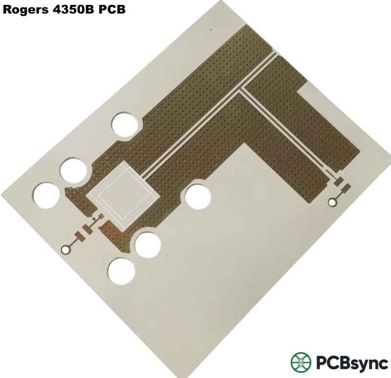
Rogers Corporation manufactures a diverse portfolio of high frequency laminates that have become industry standards for RF and microwave applications. These materials use ceramic-filled PTFE or hydrocarbon-ceramic composites rather than glass-reinforced epoxy.
Rogers 4000 Series (Most Popular):
The Rogers RO4000 series strikes an optimal balance between performance and manufacturability. RO4350B is particularly popular because it can be processed using standard FR4 fabrication techniques, eliminating the need for special through-hole treatments required by traditional PTFE materials.
Key advantages include:
Stable dielectric constant (3.48) across wide frequency and temperature ranges
Low dissipation factor (0.0037 @ 10 GHz) for minimal signal loss
Excellent dimensional stability with CTE matching copper
Compatible with lead-free soldering processes
Rogers 3000 Series:
PTFE ceramic-filled laminates optimized for applications requiring ultra-low loss and extreme frequency stability. The RO3003 offers a Dk of 3.00 ± 0.04, making it ideal for:
Automotive radar systems (77 GHz)
Satellite communications
Military and aerospace applications
Cellular infrastructure (4G/5G base stations)
Rogers 5000 Series (RT/duroid):
Pure PTFE composites reinforced with microfibers or ceramic fillers, offering the lowest losses available. The RT5880 provides exceptional performance for:
Millimeter wave applications (28-100 GHz)
Broadband communications
High-power RF amplifiers
Test and measurement equipment
PTFE (Teflon): Ultimate Performance
Polytetrafluoroethylene (PTFE), commonly known by the brand name Teflon, offers the best electrical performance for extreme high frequency applications. Its ultra-low dielectric constant (2.2-2.5) and extremely low loss tangent (<0.001) make it the material of choice when performance cannot be compromised.
PTFE Advantages:
Lowest dielectric loss of any PCB substrate
Exceptional frequency stability up to 100+ GHz
Minimal moisture absorption (<0.02%)
Outstanding thermal stability (Tg >327°C)
PTFE Challenges:
Processing PTFE requires specialized fabrication techniques. The material’s non-stick properties that make it excellent for cookware create challenges in PCB manufacturing:
Requires plasma treatment or sodium etching for adhesion
Drilling generates residue that must be carefully removed
Higher material cost (8-10x FR4)
Softer than FR4, requiring careful handling
Longer lead times and minimum order quantities
PTFE-based laminates are typically reserved for applications where the performance benefits justify the additional cost and complexity, such as defense radar systems, satellite transponders, and high-end test equipment.
Hybrid PCB Constructions
For cost-sensitive designs that include both high and low-frequency sections, hybrid stackups offer an intelligent compromise. These PCBs combine different materials within the same board—typically using high frequency laminates (Rogers or PTFE) only on layers carrying RF signals, while employing standard FR4 for digital control and power distribution layers.
Benefits of Hybrid Designs:
Significant cost reduction (30-50% vs full Rogers construction)
Optimized performance where needed
Maintains manufacturability with standard processes
Flexible design options for mixed-signal applications
Essential Design Guidelines for High Frequency PCBs
Designing high frequency PCBs demands attention to details that standard PCB designs can often ignore. Here are the critical guidelines that separate successful designs from problematic ones.
Impedance Control: The Foundation of Signal Integrity
Impedance control is non-negotiable in high frequency design. At frequencies above 100 MHz, PCB traces behave as transmission lines with characteristic impedance determined by trace geometry and material properties.
Target Impedance Values:
Single-ended traces: Typically 50Ω (±5% for general applications, ±3% for critical RF)
Differential pairs: 90-100Ω for USB, HDMI; 85Ω for PCIe; 100Ω for Ethernet
Key Impedance Factors:
Trace Width and Thickness: Wider traces decrease impedance, while narrower traces increase it. For a 50Ω microstrip line on Rogers RO4350B (0.254mm substrate), a typical trace width is 0.45-0.50mm with 35μm (1 oz) copper.
Dielectric Thickness: Impedance increases with greater spacing between the signal trace and reference plane. Even 0.025mm variations in dielectric thickness can shift impedance by 5-8Ω, making precision manufacturing critical.
Dielectric Constant: Lower Dk materials increase impedance for a given trace geometry. This is why Rogers materials (Dk 3.0-3.5) require wider traces than FR4 (Dk 4.2-4.5) to achieve the same impedance.
Practical Impedance Control Tips:
Use impedance calculators from your PCB manufacturer—their tools account for their specific fabrication processes and tolerances
Design for slightly wider traces when possible; trace width reduction during manufacturing is easier than addition
Specify impedance requirements clearly on fabrication drawings
For critical designs, request impedance testing via Time Domain Reflectometry (TDR)
Layer Stackup Strategy
The layer stackup significantly impacts signal integrity in high frequency designs. A well-planned stackup minimizes crosstalk, provides solid reference planes, and enables efficient thermal management.
Recommended Stackup Practices:
Place High-Speed Signals on Surface Layers: Microstrip configurations (signal on outer layer with ground plane below) offer easier impedance control and simplified routing. Surface routing also enables better heat dissipation and facilitates inspection.
Maintain Solid Reference Planes: Every high frequency signal layer should have an uninterrupted ground or power plane directly adjacent. This provides a low-impedance return path and shields signals from interference.
Symmetric Construction: Use symmetric stackups to prevent board warping during reflow. A typical 4-layer high frequency stackup:
Layer 1: RF signals (microstrip)
Layer 2: Ground plane
Layer 3: Power/ground plane
Layer 4: Control signals
Thin Dielectrics for High Frequencies: At millimeter wave frequencies (>30 GHz), thinner substrates (0.127-0.254mm) reduce dielectric losses. For 77 GHz automotive radar, substrates as thin as 0.127mm are common.
Routing Techniques for Signal Integrity
How you route traces directly impacts signal quality at high frequencies. Follow these proven practices:
Keep Traces Short: Signal radiation and coupling increase with trace length. Minimize the distance high-frequency signals travel. For signals above 5 GHz, keep critical paths under 50mm when possible.
Avoid 90-Degree Bends: Sharp corners cause impedance discontinuities and can radiate EMI. Use 45-degree angles or curved traces with radius ≥3× trace width. Modern CAD tools can automatically apply chamfered or radiused bends.
Minimize Via Count: Each via introduces approximately 0.5 pF of parasitic capacitance and 0.1-0.2 dB of insertion loss at 10 GHz. When vias are unavoidable:
Use the smallest practical via size (0.20-0.25mm diameter)
Place ground vias adjacent to signal vias for return path continuity
Remove via stubs through back-drilling for signals >5 GHz
Maintain Consistent Ground References: When signals change layers, ensure proper return current paths. If transitioning to a layer with a different reference plane, place stitching vias or capacitors to maintain current continuity.
Control Crosstalk: Electromagnetic coupling between adjacent traces causes crosstalk that degrades signal quality.
Prevention strategies:
Maintain ≥3× trace width spacing between high frequency traces (5× for ultra-sensitive signals)
Route adjacent layers perpendicular to each other
Use ground traces or guard rings to isolate critical signals
Keep minimum 30 mils from other signal types; 50 mils for clocks
Power Distribution Network (PDN) Design
High frequency circuits are particularly sensitive to power supply noise. A robust PDN is essential.
Decoupling Capacitor Strategy:
Place multiple capacitors with different values close to IC power pins to handle various frequency ranges:
Bulk capacitors (10-100μF) for low-frequency transients
Ceramic capacitors (0.1-1μF) for mid-frequency bypassing
Small capacitors (10-100pF) for high-frequency noise suppression
Placement Guidelines: Position decoupling capacitors within 5mm of IC power pins. For high-speed digital ICs, place them on the same layer as the IC to minimize inductance.
Power Plane Design: Make power planes 20H smaller than ground planes (H = dielectric thickness) to contain electromagnetic fields and reduce edge radiation. This technique can suppress 70% of RF energy leakage.
Best Practices for High Frequency PCB Manufacturing
Even the best design can fail if PCB manufacturing practices aren’t optimized for high frequency applications. Here’s what you need to know.
Material Selection Best Practices
Match Material to Application Frequency:
<1 GHz: High-quality FR4 acceptable
1-5 GHz: Rogers 4000 series recommended
5-30 GHz: Rogers 3000 series or Isola Astra
30 GHz: PTFE-based materials essential
Consider Hybrid Constructions: For cost optimization, use high frequency materials only on layers carrying RF signals. Digital control, power distribution, and low-speed interface layers can use standard FR4.
Verify Material Availability: Specialized laminates may have longer lead times (6-12 weeks) and minimum order quantities. Confirm material availability with your fabricator before finalizing designs.
Fabrication Quality Control
Impedance Testing: Request coupon testing for all impedance-controlled nets. TDR testing provides visual confirmation that impedance remains consistent along trace length.
Surface Finish Selection: Choose finishes that minimize high-frequency losses:
Immersion silver: Excellent for RF (minimal skin effect losses)
ENIG (Electroless Nickel Immersion Gold): Good for general use
Avoid HASL (Hot Air Solder Leveling): Surface unevenness affects impedance
Controlled Drilling: For PTFE materials, use specialized drill bits and parameters to prevent delamination and ensure clean through-holes.
Design for Manufacturability (DFM)
Communicate Early: Share stackup and impedance requirements with your PCB fabricator during design. They can identify potential manufacturing issues before you commit to production.
Specify Tolerances Clearly: Document all critical parameters:
Impedance targets and tolerances
Trace width/spacing requirements
Via specifications
Material specifications with grade/type
Design Rule Margins: Build safety margins into your design rules. If your fabricator’s minimum trace width is 4 mils, design with 5 mils minimum for high-frequency traces.
Testing and Validation
Prototype Testing: Always prototype high frequency designs before volume production. Test key parameters:
S-parameters (S11, S21) to verify insertion loss and return loss
Time Domain Reflectometry for impedance verification
Functional testing at target frequency ranges
Thermal Testing: Verify thermal performance under operating conditions. Use thermal cameras to identify hot spots and validate thermal via effectiveness.
EMI Testing: Conduct electromagnetic interference testing to ensure your design meets regulatory requirements (FCC, CE) for radiated and conducted emissions.
Real-World Applications of High Frequency PCBs
Understanding where high frequency PCBs excel helps contextualize design requirements.
5G and Wireless Communications
The rollout of 5G networks operating at 28 GHz and 39 GHz mmWave frequencies demands high frequency PCBs in:
Base station antennas and RF front-ends
Small cell infrastructure
Massive MIMO antenna arrays
Beamforming modules
These applications require ultra-low loss materials (Rogers 3003, PTFE) and precise impedance control to maintain signal integrity over antenna arrays with hundreds of elements.
Automotive Radar Systems
Modern vehicles incorporate multiple radar sensors operating at 77 GHz for:
Adaptive cruise control
Collision avoidance
Blind spot detection
Parking assistance
These systems use thin (0.127-0.254mm) high frequency substrates with tight impedance tolerances (±3%) to achieve the performance needed for life-critical applications.
Satellite and Aerospace Communications
Satellite transponders, ground station equipment, and aircraft communication systems operate across wide frequency ranges (1-40 GHz). Requirements include:
Extreme temperature stability (-55°C to +125°C)
Low outgassing for space applications
High reliability (>20 year lifetime)
Radiation tolerance
PTFE-based laminates and specialty aerospace-grade materials dominate these applications.
Medical Imaging Equipment
MRI systems, ultrasound devices, and medical diagnostic equipment use high frequency electronics for:
RF coil assemblies (operating at 64-128 MHz for 1.5T systems)
Signal processing boards
Phased array transducers
These applications demand low noise, excellent signal integrity, and compliance with medical device regulations.
Frequently Asked Questions (FAQs)
1. What frequency qualifies a PCB as “high frequency”?
Generally, PCBs operating above 500 MHz are considered high frequency, though the most common threshold is 1 GHz. At these frequencies, standard FR4 materials begin experiencing significant dielectric losses and impedance control becomes critical. The exact classification can vary by industry—telecommunications might classify anything above 1 GHz as high frequency, while defense applications might reserve the term for circuits above 10 GHz. The key indicator is whether your design requires specialized materials and controlled impedance to maintain signal integrity.
2. Can I use FR4 for high frequency applications?
FR4 can work for frequencies below 1 GHz, but with limitations. Its high dielectric constant (4.2-4.5) and dissipation factor (0.015-0.020) cause signal loss and phase distortion at higher frequencies. For cost-sensitive designs operating at 1-2 GHz, high-grade FR4 with controlled Dk might suffice, but expect degraded performance compared to Rogers materials. Above 5 GHz, FR4’s losses become prohibitive and specialized high frequency materials are essential. Hybrid constructions—using FR4 for non-critical layers and Rogers/PTFE for RF layers—offer a cost-effective compromise for many applications.
3. Why are Rogers PCBs so expensive compared to FR4?
Rogers materials cost 5-10 times more than FR4 due to several factors: specialized raw materials (ceramic-filled PTFE or hydrocarbon composites), smaller production volumes, proprietary formulations, and rigorous quality control. Additionally, Rogers maintains consistent electrical properties across frequency and temperature ranges, requiring precise manufacturing processes. However, the investment is justified for applications where signal integrity directly impacts system performance—a failed $50 communication system due to poor PCB performance costs far more than using a $300 Rogers board. For many applications, the performance benefits and reliability improvements offset the higher material cost.
4. How do I calculate impedance for my high frequency PCB design?
Impedance calculations depend on multiple factors: trace geometry (width, thickness), dielectric properties (Dk, Df), substrate height, and conductor configuration (microstrip vs stripline). While basic formulas exist, precise calculations require specialized tools. The best approach is using your PCB manufacturer’s impedance calculator—these tools account for their specific fabrication processes, materials, and tolerances. Most major fabricators provide free online calculators. Input your stackup details, target impedance, and the tool generates appropriate trace dimensions. For critical designs, request impedance testing via TDR to verify actual manufactured values match specifications.
5. What’s the difference between high frequency and high-speed PCB design?
While related, these terms describe different aspects of signal behavior. High frequency refers to the signal’s operating frequency (measured in GHz), focusing on RF and microwave applications where signals propagate as electromagnetic waves. High-speed refers to signal edge rates (measured in rise/fall time), typically describing digital signals. A 100 MHz clock with 1ns rise time is high-speed but not necessarily high frequency. However, fast edge rates contain high-frequency harmonic content—a 1ns rise time has significant energy up to 500 MHz. In practice, both domains share similar design challenges (impedance control, signal integrity, EMI) but emphasize different parameters. High frequency designs focus on RF performance and insertion loss, while high-speed designs prioritize timing, crosstalk, and signal quality at switching edges.
Conclusion: Mastering High Frequency PCB Design
High Frequency PCB design represents the intersection of material science, electromagnetic theory, and practical engineering. As wireless technologies advance and data rates increase, mastery of these principles becomes increasingly valuable for electronics professionals.
The key takeaways for successful high frequency PCB design include:
Material Selection is Foundational: Choose materials appropriate for your frequency range, with Rogers 4000 series offering the best balance of performance and manufacturability for most applications between 1-40 GHz.
Impedance Control is Non-Negotiable: At high frequencies, every trace is a transmission line. Maintain consistent impedance through careful stackup design, precise trace geometry, and close collaboration with fabricators.
Design Margins Matter: Build in safety margins for trace widths, spacing, and tolerances. What works at 1 GHz may fail at 10 GHz due to manufacturing variations.
Prototype and Test: High frequency designs often reveal surprises. Prototype early, measure thoroughly, and iterate based on actual performance data rather than simulations alone.
Partner with Experienced Fabricators: The best design can fail with poor execution. Work with PCB manufacturers experienced in high frequency applications who understand the unique requirements and can provide design feedback.
As 5G networks expand, autonomous vehicles proliferate, and IoT devices demand higher bandwidth, the demand for skilled high frequency PCB designers will only grow. Whether you’re developing your first RF project or refining advanced designs, applying these materials, guidelines, and best practices will set you on the path to success.
The future of electronics is high frequency—master these principles today to stay ahead in tomorrow’s technology landscape.
Ready to start your high frequency PCB project? Consider consulting with experienced PCB manufacturers who can review your design and provide recommendations specific to your application requirements and budget constraints.
Inquire: Call 0086-755-23203480, or reach out via the form below/your sales contact to discuss our design, manufacturing, and assembly capabilities.
Quote: Email your PCB files to Sales@pcbsync.com (Preferred for large files) or submit online. We will contact you promptly. Please ensure your email is correct.
Notes: For PCB fabrication, we require PCB design file in Gerber RS-274X format (most preferred), *.PCB/DDB (Protel, inform your program version) format or *.BRD (Eagle) format. For PCB assembly, we require PCB design file in above mentioned format, drilling file and BOM. Click to download BOM template To avoid file missing, please include all files into one folder and compress it into .zip or .rar format.


