Inquire: Call 0086-755-23203480, or reach out via the form below/your sales contact to discuss our design, manufacturing, and assembly capabilities.
Quote: Email your PCB files to Sales@pcbsync.com (Preferred for large files) or submit online. We will contact you promptly. Please ensure your email is correct.
Notes: For PCB fabrication, we require PCB design file in Gerber RS-274X format (most preferred), *.PCB/DDB (Protel, inform your program version) format or *.BRD (Eagle) format. For PCB assembly, we require PCB design file in above mentioned format, drilling file and BOM. Click to download BOM template To avoid file missing, please include all files into one folder and compress it into .zip or .rar format.
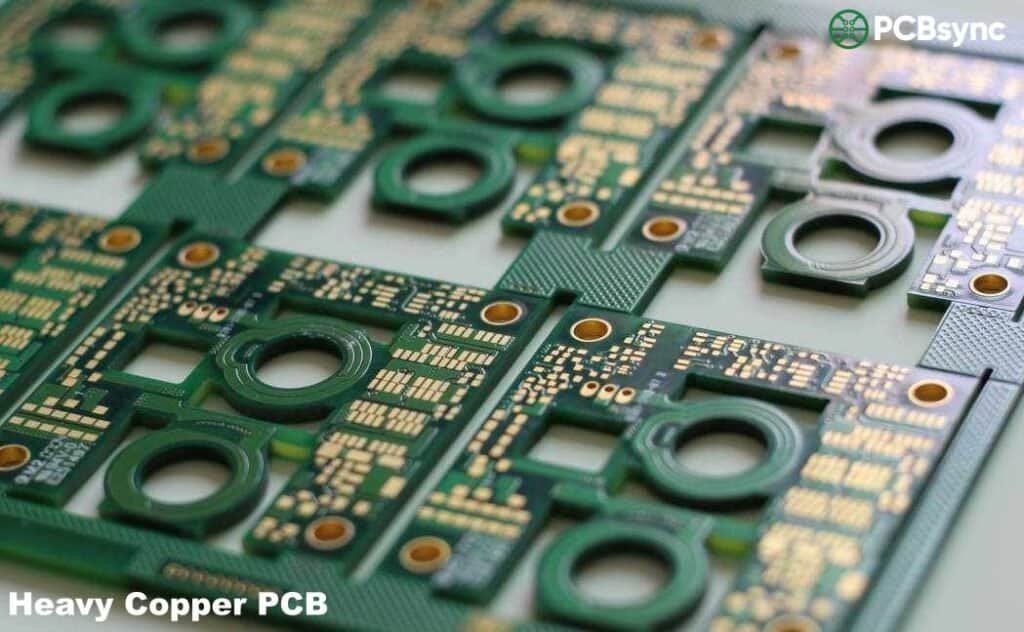
Heavy Copper PCB Manufacturing: Design Rules, Benefits & Applications Guide
When Tesla’s battery management system channels over 400 amps through circuit boards during rapid acceleration, standard PCBs would fail within seconds. The solution? Heavy copper PCB manufacturing—a specialized process that creates circuit boards capable of handling extreme power demands while maintaining reliability in the harshest conditions.
Heavy copper PCB manufacturing has revolutionized how engineers approach high-power electronics. From electric vehicle charging systems to industrial power distribution, these specialized boards enable applications that were impossible just a decade ago. This comprehensive guide explores everything you need to know about heavy copper PCB manufacturing, including critical design rules, manufacturing processes, and real-world applications.
What is Heavy Copper PCB Manufacturing?
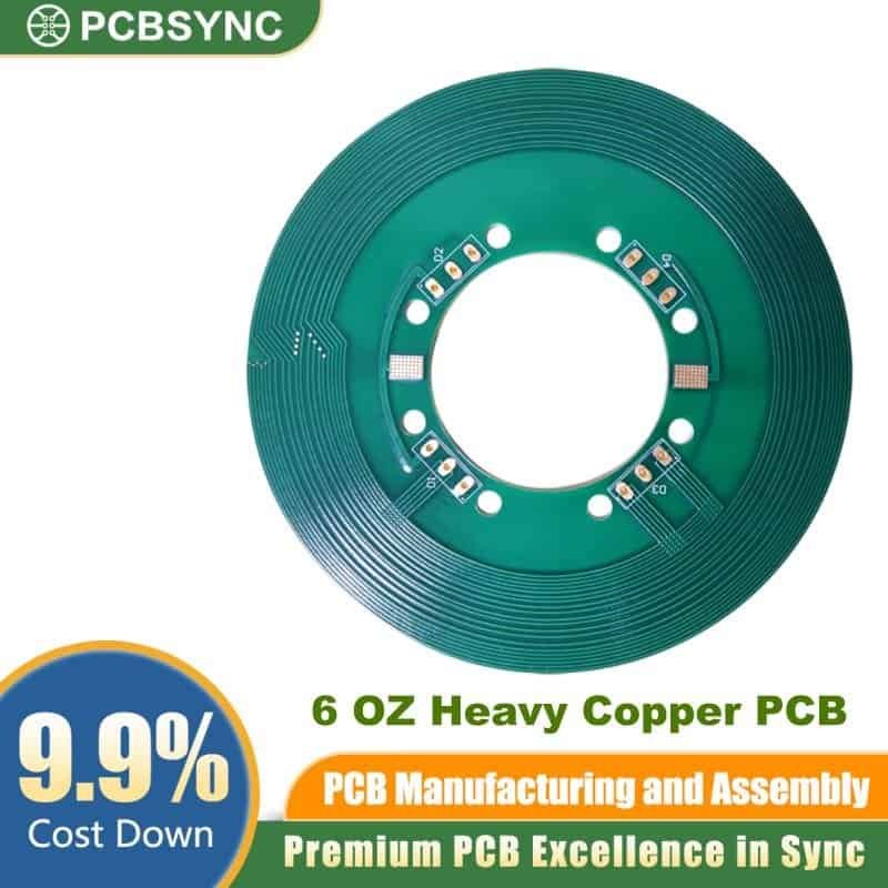
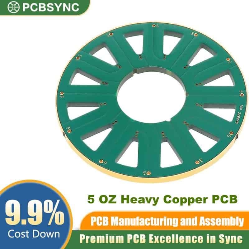
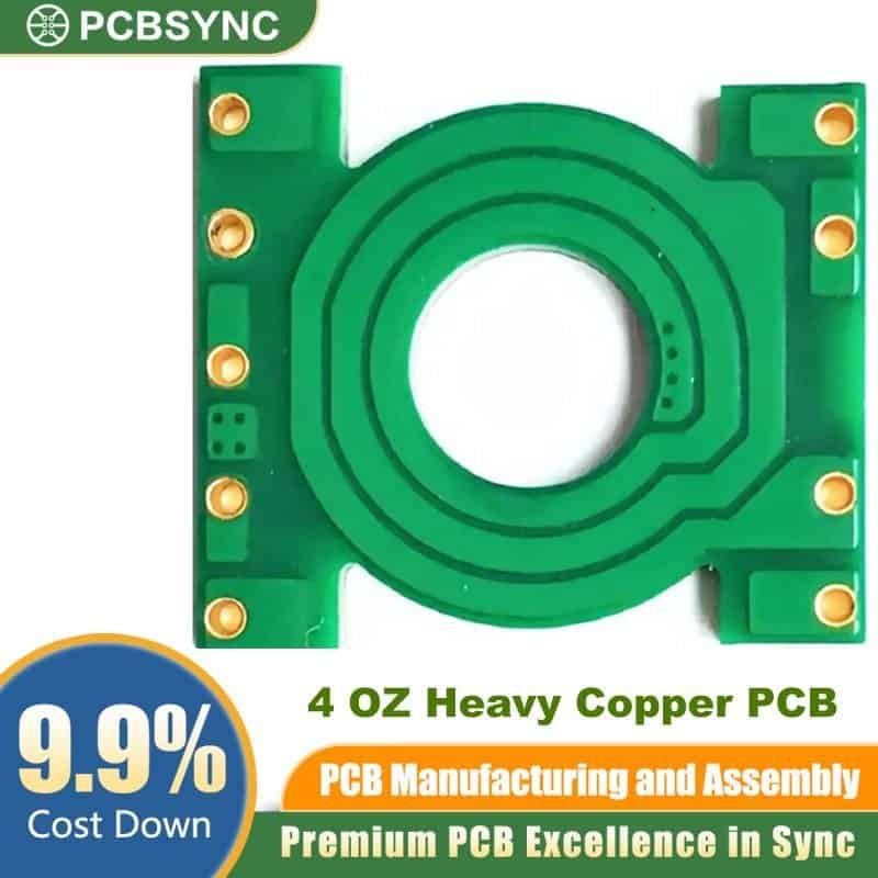
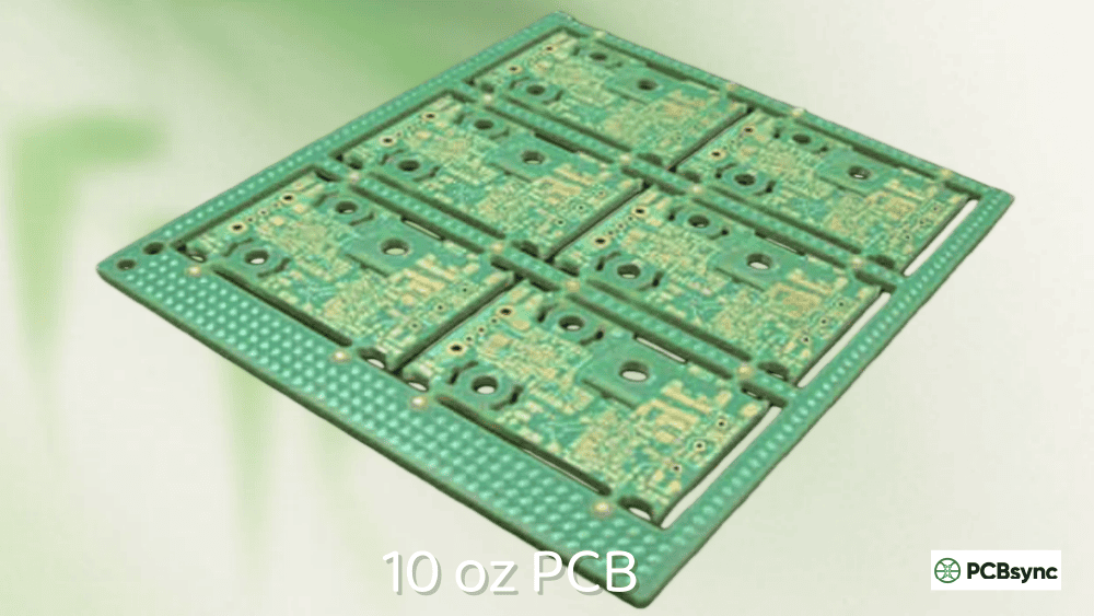
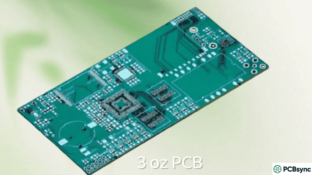
Heavy copper PCB manufacturing refers to the process of creating printed circuit boards with copper thickness of 3 ounces per square foot (oz/ft²) or greater. Unlike standard PCBs that typically use 1-2 oz copper, heavy copper boards feature significantly thicker copper layers that provide superior current-carrying capacity and thermal management.
Understanding Copper Weight Measurement
The PCB industry measures copper thickness in ounces per square foot, which correlates directly to physical thickness:
Table 1: Copper Weight to Thickness Conversion
Copper Weight
Thickness (mils)
Thickness (μm)
Current Capacity
0.5 oz
0.7 mils
17.5 μm
1-5A
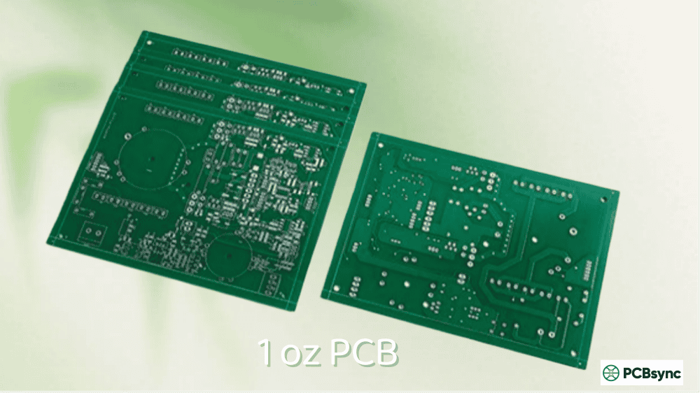
1 oz (Standard)
1.4 mils
35 μm
3-10A
2 oz
2.8 mils
70 μm
10-30A
3 oz (Heavy)
4.2 mils
105 μm
20-50A
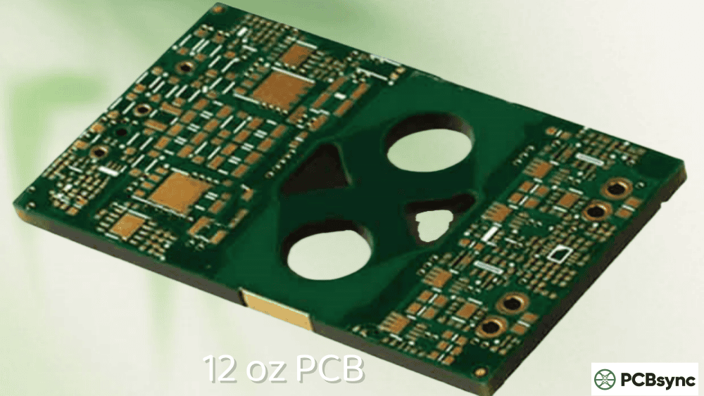
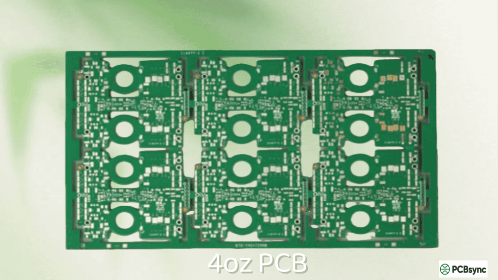
4 oz (Heavy)
5.6 mils
140 μm
50-100A
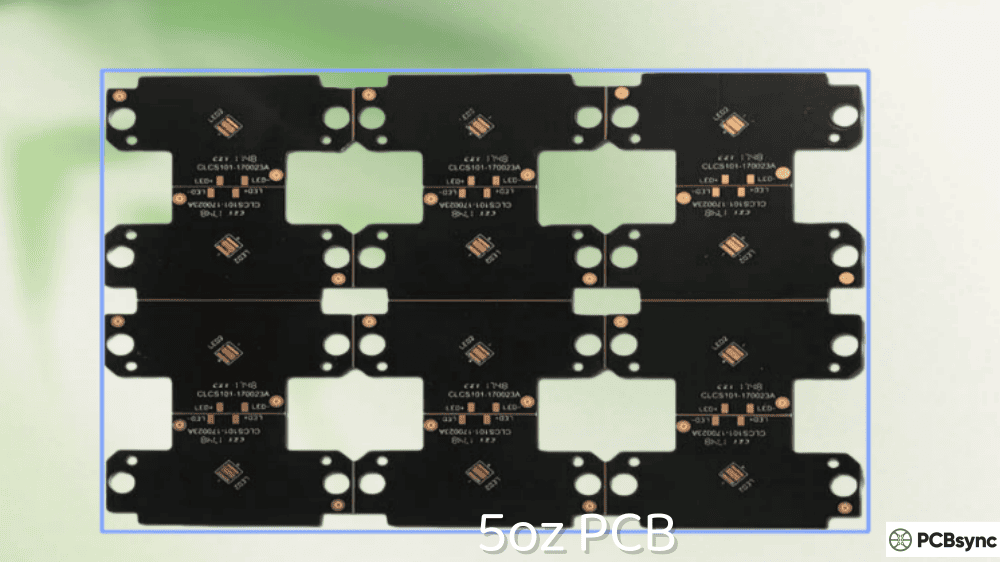
6 oz (Heavy)
8.4 mils
210 μm
100-200A
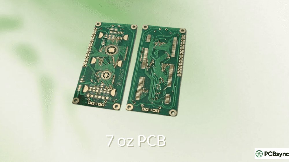
10 oz (Extreme)
14 mils
350 μm
200-500A
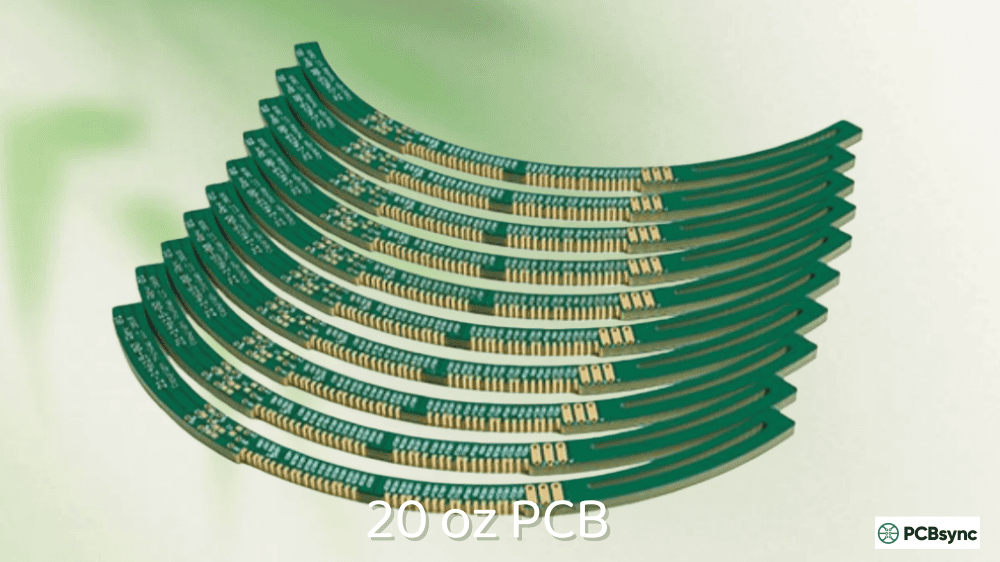
20 oz (Extreme)
28 mils
700 μm
500A+
This measurement represents the weight of copper that would cover one square foot of PCB surface, making it a universal standard across the industry.
The primary advantage of heavy copper PCB manufacturing is dramatically increased current capacity. While standard 1 oz copper traces handle 3-10 amps depending on width, heavy copper boards can safely carry 50-500 amps per layer without overheating.
Real-world impact: A 4 oz copper trace can carry 5-10 times more current than a standard 1 oz trace of the same width. This eliminates the need for bulky external conductors and enables more compact designs.
Exceptional Thermal Management
Heavy copper acts as an integrated heat sink within the PCB structure. Copper’s thermal conductivity of 401 W/(m·K) means thicker copper layers can dissipate heat 30-50% more efficiently than standard boards.
Key thermal benefits include:
Component operating temperatures reduced by 15-20°C
Hot spot reduction of 40-60% compared to standard designs
Elimination or reduction of external heatsinks
Extended component lifespan through better thermal cycling endurance
Enhanced Mechanical Strength
Thicker copper layers provide superior mechanical properties, making heavy copper PCBs ideal for demanding environments:
20% lower failure rates in harsh environments
Better resistance to vibration and mechanical stress
Stronger plated-through holes (PTHs) and via connections
Improved connector site reliability
Design Flexibility and Space Savings
Heavy copper PCB manufacturing enables designers to consolidate multiple standard layers into fewer heavy copper layers, resulting in:
60% space reduction in power management systems
Integration of high-power and control circuits on the same board
Reduced overall layer count and manufacturing complexity
Lower total system cost despite higher PCB cost
Heavy Copper PCB Calculator
PCBSync Engineering Tools
🔄
Copper Weight Converter
Conversion Results
oz/ft²
3.00
Millimeters
0.1050
Mils
4.13
Micrometers
105.0
📊
Standard Copper Weights Reference
Weight
mm
mils
µm
Type
0.5 oz
0.0175
0.69
17.5
Standard
1 oz
0.035
1.38
35
Standard
2 oz
0.070
2.76
70
Standard
3 oz
0.105
4.13
105
Heavy
4 oz
0.140
5.51
140
Heavy
6 oz
0.210
8.27
210
Heavy
10 oz
0.350
13.78
350
Extreme
20 oz
0.700
27.56
700
Extreme
💡Heavy copper PCBs typically start at 3 oz/ft² (105µm) and can go up to 20 oz/ft² or more for extreme high-current applications like power converters and EV systems.
⚡
Current Carrying Capacity (IPC-2221)
mils
°C
Maximum Current Capacity
0Amps
Cross-Section Area
0 mm²
Resistance/Length
0 mΩ/cm
📈
Current Capacity Comparison
For 100 mil trace width @ 20°C rise (External)
1 oz
4.5A
2 oz
7.5A
3 oz
10.2A
4 oz
12.5A
6 oz
16.5A
10 oz
23.2A
20 oz
35.8A
⚠️IPC-2221 provides conservative estimates. Actual capacity depends on ambient temperature, nearby traces, airflow, and PCB material. Add 20-30% safety margin for production designs.
📐
Trace Width Calculator
Amps
°C
Minimum Trace Width Required
0mils
In Millimeters
0 mm
Recommended Width
0 mils
🔍
Visual Trace Comparison
Trace width needed for 15A @ 20°C rise
1 oz Copper680 mils (17.3mm)
3 oz Copper165 mils (4.2mm)
6 oz Copper68 mils (1.7mm)
10 oz Copper35 mils (0.9mm)
✨Heavy copper allows significantly narrower traces for the same current, enabling more compact high-power PCB designs and better routing flexibility.
🌡️
Thermal Resistance Calculator
mm²
Watts
Thermal Analysis Results
Thermal Conductivity
0 W/(m·K)
Est. Temperature Rise
0 °C
Thermal Spreading
–
📋
Thermal Properties Comparison
Copper Thermal Conductivity385 W/(m·K)
FR-4 Thermal Conductivity0.25 W/(m·K)
Aluminum (for comparison)205 W/(m·K)
Copper vs FR-4 Ratio1540x better
PCB Layer Stack Visualization
Heavy copper increases thermal mass and heat spreading capability
🔥Heavy copper acts as an integrated heatsink. For optimal thermal management, use thermal vias to connect copper planes across layers, creating 3D heat spreading paths.
💰
Heavy Copper PCB Cost Estimator
mm
mm
Estimated Cost Range
$0
Per Unit Cost
$0
Cost Multiplier
1.0x
📊
Cost Factors Breakdown
Relative cost impact of heavy copper vs standard PCB
Copper Material+40-200%
Etching Process+30-80%
Drilling+20-50%
Plating+25-60%
Lead Time+3-7 days
💡Heavy copper PCBs typically cost 2-5x more than standard PCBs. The exact cost depends on copper weight, trace/space requirements, and manufacturing complexity. Contact PCBSync for accurate quotes.
Click on each tip to expand detailed design guidelines for heavy copper PCBs.
1Trace Width & Spacing▼
Minimum Trace Width: Heavy copper requires wider minimum traces due to etching undercut. For 3oz copper, minimum trace is typically 8-10 mils; for 6oz, it’s 12-15 mils; for 10oz+, expect 20+ mils minimum.
Spacing Rules: Increase spacing proportionally with copper weight. Use 1:1 ratio as a starting point (trace width = spacing). For high voltage, increase spacing per IPC-2221 guidelines.
Tip: Design with 20% margin above minimums to improve yield and reduce cost.
2Via Design▼
Via Size: Use larger vias for heavy copper (minimum 0.4mm drill for 3oz, 0.5mm for 6oz+). The aspect ratio (board thickness/hole diameter) should not exceed 8:1.
Via Arrays: For high current, use multiple vias in parallel. Calculate total current capacity as sum of individual via capacities minus 20% for thermal coupling.
Thermal Vias: Place thermal vias directly under heat-generating components with 0.3-0.5mm pitch. Fill with solder or conductive epoxy for best thermal transfer.
3Layer Stackup▼
Symmetrical Design: Always use symmetrical copper distribution to prevent board warping. If outer layers are 4oz, balance with inner power/ground planes.
Prepreg Selection: Use high-resin content prepreg (≥60%) to fill the gaps caused by thick copper features. Multiple prepreg sheets may be needed.
Mixed Copper: Consider using heavy copper only where needed (power paths) and standard copper for signal layers to optimize cost and manufacturability.
4Solder Mask▼
Coverage Challenges: Heavy copper creates significant height differences. Standard solder mask may not adequately cover trace edges, leading to exposed copper.
Solutions: Request multiple solder mask coats, use liquid photoimageable (LPI) solder mask, or consider selective solder mask with exposed copper planes for better thermal performance.
Design Rule: Increase solder mask clearance by 2-3 mils per ounce of copper above 2oz to account for registration challenges.
5Thermal Management▼
Copper Planes: Maximize copper pour areas for heat spreading. Use polygon pours connected to power components. Avoid isolated copper islands that can’t dissipate heat.
Component Placement: Distribute heat sources evenly. Keep high-power components away from board edges where heat can’t spread in all directions.
Airflow: Orient traces parallel to expected airflow direction. Place thermal relief patterns on pads connected to large copper areas for reliable soldering.
6Etching Considerations▼
Undercut Effect: Thick copper etches more at the base than the top, creating trapezoidal trace profiles. Plan for ~1mil undercut per ounce of copper on each side.
Compensation: Work with your fab to determine etch compensation factors. Typically add 0.5-1.0 mils per ounce to designed trace widths.
Isolation: Large copper areas may need isolation slots or breakup patterns to ensure complete etching and prevent shorts from bridged copper.
7DFM Guidelines▼
Panelization: Heavy copper boards need larger panel margins and breakaway tabs due to increased mechanical stress during depaneling.
Tooling Holes: Use larger tooling holes (≥3.2mm) with adequate clearance from copper features to prevent damage during handling.
Documentation: Clearly specify copper weights for each layer in fab notes. Include cross-section drawings for complex stackups. Communicate current requirements to help fab optimize the design.
8Testing & Verification▼
Electrical Testing: Request 100% electrical testing for heavy copper boards due to higher risk of shorts from etching challenges.
Cross-Section Analysis: For critical applications, request cross-section samples to verify copper thickness, via plating quality, and layer registration.
Thermal Cycling: Heavy copper PCBs may experience different thermal expansion. Consider thermal cycling tests for high-reliability applications to verify long-term solder joint integrity.
📞For accurate quotes and DFM review of your heavy copper PCB design, contact PCBSync engineering team. We provide free design review and optimization suggestions for complex high-power applications.
Critical Design Rules for Heavy Copper PCB Manufacturing
Successful heavy copper PCB manufacturing requires adherence to specific design rules that differ significantly from standard PCB design. Understanding these rules early in the design phase prevents costly redesigns and manufacturing delays.
Minimum Trace Width and Spacing Requirements
As copper thickness increases, both minimum trace width and spacing must increase proportionally due to the etching process. Thicker copper requires deeper etching, which creates more undercutting.
Table 2: Trace Width and Spacing Design Rules by Copper Weight
Copper Weight
Min Trace Width
Min Spacing
Typical Trace Width
Typical Spacing
0.5 oz
3 mils
3 mils
5 mils
5 mils
1 oz
4 mils
4 mils
6 mils
6 mils
2 oz
6 mils
6 mils
8-10 mils
8-10 mils
3 oz
8 mils
8 mils
12-15 mils
12-15 mils
4 oz
10 mils
10 mils
15-20 mils
15-20 mils
6 oz
14 mils
14 mils
20-25 mils
20-25 mils
10 oz
20 mils
20 mils
30-40 mils
30-40 mils
Important note: These are general guidelines. Always consult your PCB manufacturer early in the design process, as capabilities vary between facilities.
Via Sizing and Design Considerations
Heavy copper PCB manufacturing requires larger vias than standard designs to accommodate the significant copper plating thickness in holes.
Via design rules for heavy copper:
Minimum drill size before plating: 0.025″ (25 mils) for 3-6 oz copper
Preferred drill size: 0.030″ (30 mils) or larger
Via aspect ratio: Maximum 8:1 for reliable plating
Re-drilling: Often required after plating to achieve final hole dimensions
For vias carrying high current, calculate cross-sectional area using:
Class 2 plating: 20 microns (0.0008″) wall thickness
Class 3 plating: 25 microns (0.0010″) wall thickness
Current Capacity Calculations
Determining the correct trace width for your current requirements is essential in heavy copper PCB manufacturing. Use IPC-2152 or IPC-2221 standards as a foundation.
Table 3: Trace Width for Common Current Loads (External Layers)
Current (A)
1 oz Copper
2 oz Copper
4 oz Copper
Temperature Rise
1A
10 mils
5 mils
3 mils
10°C
3A
40 mils
20 mils
10 mils
10°C
5A
80 mils
40 mils
20 mils
10°C
10A
200 mils
100 mils
50 mils
10°C
20A
500 mils
250 mils
125 mils
10°C
50A
1500 mils
750 mils
375 mils
10°C
Critical considerations:
Internal layers carry only 50% of external layer capacity at the same temperature rise
Wider traces or increased copper weight can achieve the same current capacity
Always design for a maximum 30°C temperature rise for reliability
Copper Distribution and Balance
Proper copper distribution is crucial in heavy copper PCB manufacturing to prevent warping and ensure uniform processing.
Best practices:
Distribute copper evenly across the entire board area
Use the same copper weight on mirror opposite layers (e.g., Layer 1 and Layer 4)
Avoid large areas of isolated copper surrounded by open space
Consider copper thieving patterns in areas with low copper density
Understanding the manufacturing process helps designers create boards that are both manufacturable and cost-effective.
Step 1: Material Selection and Preparation
Heavy copper PCB manufacturing begins with selecting appropriate base materials:
Common substrate materials:
FR-4 Standard: Tg 130-140°C for most applications
High Tg FR-4: Tg 170-180°C for high-temperature applications
Polyimide: Tg 250°C+ for extreme environments
Rogers/Ceramic: For RF and high-frequency applications
Copper foil selection depends on the manufacturing method. Starting with lighter base copper (0.5-1 oz) and plating up provides better trace definition than using heavy base foil.
Step 2: Imaging and Etching
The imaging process transfers the circuit pattern to the copper using photoresist:
Apply photoresist to copper-clad laminate
Expose through photomask using UV light
Develop to remove unexposed resist
Etch to remove unprotected copper
Critical challenge: Heavy copper requires significantly longer etching times, creating deeper undercuts. Modern manufacturers use differential etching techniques and etch compensation to achieve straighter sidewalls.
Etch factor compensation for different copper weights:
0.5 oz: Add 0.001″ to trace width
1 oz: Add 0.0015-0.002″ to trace width
2 oz: Add 0.0025-0.003″ to trace width
3 oz+: Consult manufacturer for specific compensation
Step 3: Electroplating
Electroplating is the defining process in heavy copper PCB manufacturing. This step builds up copper thickness in plated-through holes and on trace sidewalls.
Plating methods:
Pattern plating: Most common; builds up copper only in circuit areas
Panel plating: Plates entire panel, then etches away excess
Step plating: Multiple plating cycles for extreme copper thickness
For extreme copper (10 oz+), plating may require 20+ hours to achieve the desired thickness.
Heavy copper PCB manufacturing demands rigorous testing:
Electrical testing: Continuity and isolation testing at 100% coverage
Microsectioning: Verify copper thickness and via plating quality
Thermal cycling: Ensure reliability under temperature stress
Impedance testing: For controlled impedance designs
Visual inspection: Check for defects and workmanship quality
Applications of Heavy Copper PCB Manufacturing
Heavy copper PCB manufacturing serves critical applications across multiple industries where reliability, high current capacity, and thermal performance are non-negotiable.
Power Electronics
Applications include:
Power supplies: Server and telecom power systems handling 20-100A
Inverters: Solar and wind power conversion systems up to 500A
DC-DC converters: High-efficiency power conversion
Battery management systems: EV and energy storage applications
Typical requirements: 4-10 oz copper, high Tg materials, excellent thermal management
Automotive Industry
The automotive sector, particularly electric vehicles, relies heavily on heavy copper PCB manufacturing:
EV battery management: Monitoring and control of high-voltage battery packs
Motor controllers: Managing 200-400A for propulsion motors
DC-DC converters: Converting high-voltage battery power to 12V systems
Charging systems: On-board and off-board charging electronics
Industry trend: The global EV market is driving 25-30% annual growth in heavy copper PCB demand.
Industrial Control Systems
Manufacturing and industrial applications require robust, reliable heavy copper PCBs:
Variable frequency drives (VFDs): Motor control for pumps, fans, conveyors
Welding equipment: High-current power delivery systems
Industrial robotics: Servo motor controllers and power distribution
Process control: Safety and monitoring systems
Renewable Energy Systems
Solar power applications:
Photovoltaic inverters handling 50-100A continuous current
Maximum Power Point Tracking (MPPT) controllers
Grid-tie systems requiring high reliability
Wind power applications:
Turbine power converters
Grid integration systems
Pitch control systems
Aerospace and Defense
Military and aerospace applications demand the highest reliability:
Radar systems: High-power RF transmission
Weapons control: Mission-critical power distribution
Avionics: Flight control and navigation systems
Communication systems: High-frequency, high-power transmission
Requirements: Often require 6-20 oz copper with polyimide substrates for extreme temperature ranges.
Medical Equipment
High-power medical devices benefit from heavy copper PCB manufacturing:
X-ray machines: High-voltage, high-current power supplies
MRI systems: Gradient coil drivers requiring precise current control
Surgical equipment: Electrocautery and laser systems
Imaging equipment: CT scanners and other diagnostic tools
Heavy Copper vs Standard PCB: Complete Comparison
Understanding when to specify heavy copper PCB manufacturing versus standard PCB fabrication is essential for optimal design.
Table 4: Comprehensive Comparison – Heavy Copper vs Standard PCB
Feature
Standard PCB (1-2 oz)
Heavy Copper PCB (3-20 oz)
Copper Thickness
35-70 μm (1.4-2.8 mils)
105-700 μm (4.2-28 mils)
Current Capacity
3-30A typical
50-500A+
Thermal Performance
Standard
30-50% better heat dissipation
Temperature Rise
Higher for same current
15-20°C lower for same current
Mechanical Strength
Standard
20%+ stronger, better vibration resistance
Min Trace/Space
3-4 mils / 3-4 mils
8-20 mils / 8-20 mils
Manufacturing Time
5-10 days typical
10-15 days typical
Cost
Lower (baseline)
2-5x higher
Plating Time
1-2 hours
10-20+ hours for extreme copper
Design Complexity
Simpler, standard rules
Requires specialized design rules
Applications
Consumer electronics, IoT, computing
Power electronics, automotive, industrial
Failure Rate
Baseline
20% lower in harsh environments
Layer Count Options
1-32+ layers
Typically 2-8 layers
Via Aspect Ratio
Up to 12:1
Maximum 8:1
Minimum Hole Size
0.008-0.012″
0.020-0.050″
When to Choose Heavy Copper PCB Manufacturing
Select heavy copper when your application requires:
✓ High current loads: Greater than 10 amps continuous ✓ Thermal challenges: Components generating significant heat ✓ Harsh environments: Vibration, temperature cycling, mechanical stress ✓ Reliability critical: Aerospace, medical, automotive safety systems ✓ Space constraints: Replacing multiple standard layers with fewer heavy copper layers ✓ Long service life: 10+ year operational lifetime requirements
When Standard PCB is Sufficient
Use standard 1-2 oz copper for:
✓ Low-current applications (under 5 amps) ✓ Signal processing and control circuits ✓ Consumer electronics with cost sensitivity ✓ Designs requiring fine-pitch components ✓ High-density routing with tight trace spacing
Cost Considerations in Heavy Copper PCB Manufacturing
While heavy copper PCB manufacturing costs 2-5x more than standard PCBs, total system cost may actually decrease due to:
Direct cost savings:
Elimination of external heatsinks and cooling fans
Reduced layer count (one heavy copper layer replaces multiple standard layers)
Lower failure rates minimize field service requirements
Compact designs reduce enclosure size and shipping costs
Improved thermal performance extends component life
Cost optimization strategies:
Use heavy copper only on layers that require it (hybrid constructions)
Optimize trace widths to minimum requirements
Order in appropriate quantities to achieve volume pricing
Work with manufacturers experienced in heavy copper
Manufacturing Partnerships and Quality Standards
Successful heavy copper PCB manufacturing requires choosing the right manufacturing partner.
Key Manufacturer Capabilities to Verify
✓ Maximum copper weight: Verify they can handle your requirements (3-20+ oz) ✓ Layer count capability: Especially for multilayer heavy copper designs ✓ Minimum feature sizes: Confirm they meet your design rules ✓ Testing capabilities: Electrical testing, microsectioning, thermal analysis ✓ Certifications: ISO 9001, IPC-6012 Class 2 or 3, automotive (IATF 16949), aerospace (AS9100)
Industry Standards and Certifications
Heavy copper PCB manufacturing should comply with:
IPC-2221: Generic PCB design standard
IPC-6012: Qualification and performance specification for rigid PCBs
IPC-A-600: Acceptability of printed boards
UL 94: Flammability testing for safety-critical applications
RoHS: Environmental compliance for lead-free manufacturing
Frequently Asked Questions (FAQs)
1. What is the difference between heavy copper and thick copper PCB?
Heavy copper and thick copper are interchangeable terms referring to PCBs with copper thickness of 3 oz/ft² or greater. Some manufacturers distinguish “extreme copper” as 20 oz and above, but there’s no universal standard. The terms describe the same fundamental technology: PCBs with significantly thicker copper layers than standard 1-2 oz boards, designed for high-current and high-power applications.
2. How much does heavy copper PCB manufacturing cost compared to standard PCB?
Heavy copper PCB manufacturing typically costs 2-5 times more than standard PCBs, depending on copper weight, layer count, and complexity. A standard 4-layer PCB with 1 oz copper might cost $50-100 for prototypes, while the same design with 4 oz heavy copper could cost $200-400. However, total system cost may be lower due to eliminated external components, reduced layer count, and improved reliability reducing warranty costs.
3. Can I mix heavy copper and standard copper on the same PCB?
Yes, modern heavy copper PCB manufacturing techniques allow mixing copper weights on the same board through a process called “PowerLink” or hybrid copper construction. You can have 4-6 oz copper on high-current power layers while using 1-2 oz copper on signal and control layers. This approach optimizes cost while maintaining performance where needed. Discuss this option early with your manufacturer as it requires specialized processing.
4. What is the maximum current a heavy copper PCB can handle?
Current capacity depends on copper weight, trace width, and acceptable temperature rise. As a general guide: 4 oz copper can handle 50-100A, 6 oz copper handles 100-200A, and 10 oz copper can exceed 500A per layer. For currents above 100A, consider copper bus bars integrated into the PCB. Use IPC-2152 calculators for precise current capacity calculations based on your specific design parameters, including trace geometry and ambient temperature.
5. How long does heavy copper PCB manufacturing take?
Heavy copper PCB manufacturing typically requires 10-15 business days for prototypes, compared to 5-10 days for standard PCBs. The extended time is due to longer electroplating cycles (10-20+ hours for extreme copper), additional re-drilling steps, and more extensive quality testing. Production quantities may require 3-4 weeks. For time-critical projects, work with manufacturers offering expedited services, though this increases cost. Always allow extra time for design review and DFM (Design for Manufacturability) feedback.
Conclusion: Maximizing Success in Heavy Copper PCB Manufacturing
Heavy copper PCB manufacturing represents a critical enabling technology for modern high-power electronics. From electric vehicle battery management systems channeling hundreds of amps to industrial motor controllers operating in harsh environments, these specialized boards make possible applications that would fail with standard PCB technology.
Key takeaways for successful heavy copper PCB projects:
Design phase: Start with proper design rules, including appropriate trace widths, spacing, and via sizing. Consult your manufacturer early—during the routing phase, not after layout is complete.
Manufacturing selection: Partner with experienced manufacturers who understand heavy copper processing, have appropriate certifications, and can provide DFM feedback.
Cost optimization: Use heavy copper only where needed, consider hybrid constructions, and evaluate total system cost including eliminated components.
Testing and validation: Invest in proper prototyping and testing, including thermal cycling and electrical validation, before production.
The future of heavy copper PCB manufacturing is bright, driven by electrification trends in automotive, growth in renewable energy, and increasing power density requirements across all electronics sectors. By understanding the design rules, manufacturing processes, and application requirements outlined in this guide, you’re equipped to make informed decisions and create successful heavy copper PCB designs.
Ready to start your heavy copper PCB project? Contact experienced PCB manufacturers with your specifications, request a DFM review, and leverage their expertise to optimize your design for manufacturability, performance, and cost. The investment in proper heavy copper PCB manufacturing will pay dividends in product reliability, performance, and long-term success.
Inquire: Call 0086-755-23203480, or reach out via the form below/your sales contact to discuss our design, manufacturing, and assembly capabilities.
Quote: Email your PCB files to Sales@pcbsync.com (Preferred for large files) or submit online. We will contact you promptly. Please ensure your email is correct.
Notes: For PCB fabrication, we require PCB design file in Gerber RS-274X format (most preferred), *.PCB/DDB (Protel, inform your program version) format or *.BRD (Eagle) format. For PCB assembly, we require PCB design file in above mentioned format, drilling file and BOM. Click to download BOM template To avoid file missing, please include all files into one folder and compress it into .zip or .rar format.


