Inquire: Call 0086-755-23203480, or reach out via the form below/your sales contact to discuss our design, manufacturing, and assembly capabilities.
Quote: Email your PCB files to Sales@pcbsync.com (Preferred for large files) or submit online. We will contact you promptly. Please ensure your email is correct.
Notes: For PCB fabrication, we require PCB design file in Gerber RS-274X format (most preferred), *.PCB/DDB (Protel, inform your program version) format or *.BRD (Eagle) format. For PCB assembly, we require PCB design file in above mentioned format, drilling file and BOM. Click to download BOM template To avoid file missing, please include all files into one folder and compress it into .zip or .rar format.
HDI PCB Design and Manufacturing: From Basics to Advanced Techniques
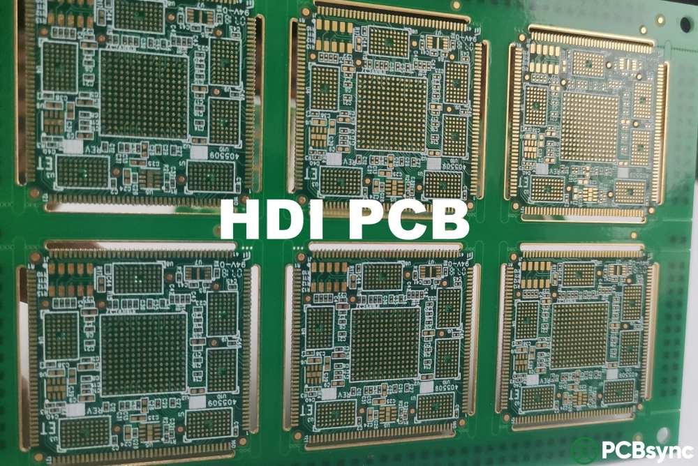
The demand for smaller, faster, and more capable electronic devices has never been higher. Your smartphone can now perform tasks that required room-sized computers just decades ago, yet it fits comfortably in your pocket. Behind this remarkable miniaturization lies a critical technology: High-Density Interconnect (HDI) printed circuit boards.
HDI PCB technology represents a fundamental shift in how we design and manufacture circuit boards. Unlike traditional PCBs that rely on through-hole vias and conventional drilling methods, HDI boards employ advanced techniques like laser-drilled microvias, sequential lamination, and ultra-fine trace routing to achieve unprecedented component density. This technology has become indispensable across industries, from consumer electronics to aerospace systems.
Whether you’re an engineer evaluating HDI for your next project, a product designer seeking to understand manufacturing constraints, or a business leader exploring advanced PCB solutions, this comprehensive guide will walk you through everything you need to know about HDI PCB design and manufacturing.
Understanding HDI PCB: Definition and Core Characteristics
High-Density Interconnect PCBs are multilayer circuit boards characterized by significantly higher wiring density per unit area compared to conventional printed circuit boards. According to IPC-2226 standards, an HDI PCB typically features:
Fine lines and spaces measuring 100 micrometers (0.10mm) or less
Microvias with diameters smaller than 150 micrometers
Capture pads under 400 micrometers (0.40mm)
Connection pad density exceeding 20 pads per square centimeter
What distinguishes HDI PCBs from standard boards is their use of blind vias (connecting outer layers to inner layers), buried vias (connecting only inner layers), and microvias (extremely small interconnections typically created by laser drilling). This via architecture enables routing paths that would be impossible with conventional through-hole technology.
The technology emerged in the 1980s when researchers began investigating methods to reduce via sizes in PCBs. The first production build-up boards appeared in 1984, and since then, HDI technology has evolved to meet the ever-increasing demands for miniaturization and performance. Today, HDI manufacturing follows established standards including IPC-2315, IPC-2226, IPC-4104, and IPC-6016.
Via Fill RecommendationCopper filled (via-in-pad capable)
Plating DifficultyStandard
Impedance Calculator
50.0Ω
Target Impedance Match50Ω ± 10% ✓
Propagation Delay~6.8 ps/mm
Effective Dk3.2
Note: These calculations are approximations based on empirical formulas. For production designs, always verify with your PCB manufacturer’s impedance modeling tools and request controlled impedance manufacturing.
HDI PCB Cost Estimator
Cost Breakdown
Base PCB Cost
$120
per board
HDI Premium
+45%
complexity factor
Via Processing
$35
per board
Surface Finish
$15
per board
Total Estimated Cost
Unit Price$185
Total Order Cost$18,500
Estimated Lead Time15-20 working days
Disclaimer: This is a rough estimate for budgeting purposes only. Actual pricing depends on design complexity, DFM requirements, material availability, and manufacturer capabilities. Request a formal quote for accurate pricing.
HDI PCB Design for Manufacturing (DFM) Guidelines
Microvia Aspect Ratio: Keep aspect ratio ≤ 1:1 for laser-drilled microvias. Standard is 0.8:1 for reliable plating. Max drill depth is typically 150µm.
Pad Size for Microvias: Capture pad should be ≥ via diameter + 100µm. For 100µm microvia, use minimum 200µm pad diameter.
Stacked vs Staggered Microvias: Stacked microvias require copper filling; staggered is more reliable and cost-effective. Minimum stagger offset: 150µm.
Via-in-Pad Design: Use copper-filled and planarized vias for BGA fanout. Ensure ±5µm planarity for fine-pitch components.
Layer Registration: HDI requires tighter registration tolerances (±25-50µm). Account for this in pad/annular ring sizing.
Copper Balance: Maintain copper balance across layers to prevent warpage. Aim for 40-60% copper coverage per layer.
Trace Width & Spacing Guidelines
HDI Class
Min Trace (mil)
Min Space (mil)
Min Via (µm)
Application
Standard HDI
3.5 – 4
3.5 – 4
100 – 150
Consumer electronics
Advanced HDI
2.5 – 3
2.5 – 3
75 – 100
Mobile, wearables
Ultra HDI
1.5 – 2
1.5 – 2
50 – 75
Advanced mobile, SiP
Substrate-like
< 1.5
< 1.5
< 50
IC substrates, interposers
Common DFM Issues & Solutions
Microvia Failure: Caused by excessive aspect ratio or poor fill. Solution: Reduce via depth or increase diameter; specify copper fill requirements.
Registration Errors: Inner layer misalignment affects via connections. Solution: Increase capture pad size; use fiducials on every layer.
Delamination: Caused by moisture absorption or thermal stress. Solution: Specify appropriate Tg material; include proper baking requirements.
Signal Integrity Issues: Impedance variations due to process tolerances. Solution: Request impedance testing; allow ±10% tolerance in design.
BGA Escape Routing: Insufficient via density for fine-pitch BGAs. Solution: Use dog-bone fanout with via-in-pad; consider stacked microvias for ≤0.5mm pitch.
Copper Cracking: Thermal expansion mismatch in filled vias. Solution: Use appropriate fill material; follow IPC-4761 guidelines.
Pro Tip: Always engage your PCB manufacturer early in the design process. They can provide specific DFM guidelines based on their process capabilities and help optimize your design for yield and cost.
Annular Ring Calculator
Annular Ring Analysis
Nominal Annular Ring100 µm
Minimum Annular Ring (Worst Case)50 µm
IPC Class 2 Requirement50 µm minimum ✓
IPC Class 3 Requirement75 µm minimum ✗
RecommendationIncrease pad to 0.45mm for Class 3
Annular Ring Reference
IPC Class
External Layers
Internal Layers
Application
Class 1
No minimum*
No minimum*
Consumer products
Class 2
50 µm (2 mil)
25 µm (1 mil)
Industrial, computers
Class 3
75 µm (3 mil)
50 µm (2 mil)
Military, aerospace, medical
*Class 1 allows breakout but must maintain minimum 90° connection
Key Technical Specifications
Modern HDI PCBs push the boundaries of what's possible in circuit board design:
Trace Width and Spacing: Advanced HDI designs can achieve trace widths as narrow as 75 micrometers (3 mils) or less, with corresponding spacing between conductors. This fine-pitch capability allows for significantly more routing density compared to standard PCBs that typically use 150-200 micrometer traces.
Via Technology: Microvia diameters typically range from 75 to 150 micrometers (3-6 mils), dramatically smaller than the 250-400 micrometer drill sizes common in traditional PCB manufacturing. The smaller aspect ratio (depth-to-diameter ratio) of microvias, ideally less than 1:1, contributes to improved reliability and signal integrity.
Layer Count: HDI technology enables board designs that would require 8-10 layers using traditional methods to be accomplished in just 4-6 HDI layers, reducing overall board thickness while maintaining or improving functionality.
Manufacturing HDI PCBs requires specialized equipment, advanced materials, and precise process control. The sequential lamination method is the cornerstone of HDI production, differentiating it fundamentally from conventional PCB manufacturing.
Sequential Lamination: Building Boards Layer by Layer
Sequential lamination, also known as sequential build-up (SBU), is the process of fabricating a multilayer PCB by adding and laminating subsets of layers in multiple stages rather than pressing all layers simultaneously. This approach enables the integration of complex via structures that define HDI technology.
Stage 1: Core Preparation
The process begins with a core layer, typically a double-sided PCB made from FR-4 or high-performance laminates. Copper traces are etched onto this core using photoresist deposition, exposure, and etching processes. Through-holes are mechanically drilled and plated to establish buried vias that will connect through the core structure.
Stage 2: First Build-Up Layer
Thin dielectric material, often resin-coated copper (RCC) or prepreg material, is applied to one or both sides of the core. RCC offers distinct advantages for HDI applications, featuring ultra-thin copper foil (12-18 micrometers) anchored to a resin layer with extremely low profile characteristics. This material enables thinner PCBs and finer line/spacing geometries.
The dielectric layer is then laminated to the core under precisely controlled heat and pressure conditions. Typical lamination parameters include temperatures of 170-200°C and pressures of 200-400 psi, though exact values depend on the materials used.
Stage 3: Laser Drilling for Microvias
Unlike conventional mechanical drilling, microvia formation primarily relies on laser drilling technology. CO2 or UV lasers ablate the dielectric material with remarkable precision, creating holes as small as 75 micrometers in diameter. The laser can be controlled to stop precisely at the copper pad beneath, creating depth-controlled blind vias.
Laser drilling offers several advantages over mechanical drilling:
Capability to create much smaller hole diameters
No mechanical stress on the laminate
Faster processing for high-density via patterns
Better hole quality with minimal burrs or resin smear
The typical laser drilling rate is approximately 200-400 holes per second for CO2 lasers, though this varies based on material type and hole size requirements.
Stage 4: Via Metallization and Plating
After laser drilling, the panels undergo thorough cleaning to remove laser residue and prepare the via walls for metallization. Several methods can be used for via plating:
Electroless Copper Plating: A thin seed layer of copper is deposited chemically on the via walls, followed by electroplating to build up the copper thickness to 15-25 micrometers.
Direct Plating: Advanced processes use conductive polymers or specialized chemistry to enable direct electroplating without the electroless seed layer.
Via Filling: For stacked microvia designs or via-in-pad applications, the via is filled with conductive or non-conductive epoxy, then planarized and capped with copper plating.
Stage 5: Outer Layer Circuit Formation
Copper foil is laminated to the metallized build-up layer, and photolithography processes define the circuit patterns. After copper electroplating and tin plating for etch resist, the unwanted copper is etched away, leaving the designed conductor pattern.
Stage 6: Repeated Build-Up (If Required)
For complex HDI designs requiring multiple microvia layers (such as 2+N+2 or 3+N+3 structures), stages 2 through 5 are repeated. Each iteration adds another build-up layer with its own microvia interconnections, enabling increasingly complex routing capabilities.
Stage 7: Final Surface Finishing
After all layers are built and laminated, the board receives surface treatment to protect exposed copper and ensure solderability. Common finishes for HDI PCBs include:
OSP (Organic Solderability Preservative) - cost-effective option for single-use assembly
Immersion Silver or Tin - providing good solderability with relatively flat surfaces
Advanced Manufacturing Techniques
Laser Direct Imaging (LDI): This technology projects circuit patterns directly onto photoresist-coated panels using laser exposure, eliminating the need for physical photo tools. LDI enables tighter tolerances and faster turnaround times, making it ideal for HDI production.
Controlled Depth Drilling: For specific design requirements, controlled mechanical drilling can place vias of precise depth, though this is less common than laser drilling for HDI applications.
Chemical Via Formation: Though less frequently used, chemical etching can create vias at rates of 8,000-12,000 per second, though with less precision than laser methods.
HDI PCB Structure Types: From Basic to Advanced
HDI boards are classified into several types based on their via architecture and build-up configuration. Understanding these structures is crucial for selecting the appropriate technology for your application.
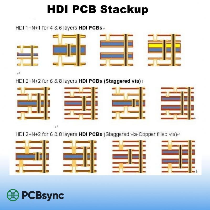
Type I HDI (1+N+1 Structure)
The most basic HDI configuration features one build-up layer on each side of a conventional core. Microvias connect the outer layers to the first inner layers, while buried vias in the core connect inner layers together. Through-holes may also pass through the entire structure.
This structure is ideal for designs requiring moderate routing density improvements over traditional PCBs. Manufacturing is relatively straightforward, with just one sequential lamination cycle beyond the core fabrication.
Type II HDI (2+N+2 Structure)
Adding complexity, Type II HDI includes two build-up layers on each side of the core. This configuration enables either staggered or stacked microvia arrangements:
Staggered Microvias: Vias on the first build-up layer and second build-up layer are offset from each other, connecting different net paths. This approach is more cost-effective and offers better reliability due to reduced stress concentration.
Stacked Microvias: Vias are aligned vertically, one on top of another, maximizing routing density but requiring copper-filled vias to maintain structural integrity and electrical continuity. Stacked vias demand precise registration and advanced filling processes, increasing manufacturing complexity and cost.
Type III HDI (3+N+3 and Higher)
Three or more build-up layers per side characterize Type III HDI, typically used in extremely complex designs like high-end smartphones and advanced computing modules. These structures may incorporate any combination of stacked, staggered, and skip vias (microvias that span multiple dielectric layers).
Any-Layer HDI and Coreless Construction
The most advanced HDI configurations include any-layer interconnect technology, where vias can connect any layer to any other layer through complex via arrangements. Coreless constructions eliminate the traditional thick core entirely, building the board entirely through sequential lamination of thin dielectric and copper layers.
These ultra-advanced structures offer maximum flexibility and density but come with significantly higher manufacturing costs and complexity.
HDI PCB Design Guidelines and Best Practices
Successful HDI design requires careful attention to manufacturability, signal integrity, and reliability. The following guidelines will help ensure your design can be manufactured efficiently while meeting performance requirements.
Via Design Strategy
Aspect Ratio Management: Maintain microvia aspect ratios below 1:1 for optimal reliability. For example, a 100-micrometer diameter via should not exceed 100 micrometers in depth. Some manufacturers claim reliability up to 2:1 aspect ratios, but conservative design practices favor lower ratios.
Via Type Selection: Choose via types based on routing requirements and cost considerations:
Blind microvias for outer-to-inner layer connections
Buried vias within the core for inner-to-inner connections
Through vias only when absolutely necessary, as they consume valuable routing space
Stacked vs. Staggered: Use staggered vias when possible to reduce cost and improve reliability. Reserve stacked vias for applications where board space is critical and the additional complexity is justified.
Via-in-Pad Technology: For fine-pitch BGA components and maximum density, via-in-pad places the microvia directly beneath the component pad. This technique requires filled and capped vias to provide a flat surface for component attachment.
Trace Width and Spacing Optimization
Current Carrying Requirements: Calculate minimum trace widths based on current requirements, considering the thinner copper weights often used in HDI designs (typically 18-35 micrometers base copper).
Manufacturing Capabilities: Consult with your fabricator early to determine their fine-line capabilities. While 75-micrometer (3 mil) lines and spaces are achievable, many facilities have minimum standards of 100-125 micrometers for improved yield.
Signal Integrity Considerations: For high-speed signals, maintain controlled impedance through careful trace width, spacing, and dielectric thickness selection. HDI's shorter routing paths inherently improve signal integrity, but proper impedance matching remains critical.
Stackup Planning
Layer Count Determination: Calculate required layer count based on:
Pin count of the largest BGA component
Total signal routing requirements
Power distribution needs
Manufacturability and cost constraints
Material Selection: Choose dielectric materials appropriate for your application:
Standard FR-4 for cost-sensitive applications
High-Tg materials (glass transition temperature >170°C) for improved reliability
Low-loss materials for high-frequency applications
Laser-drillable prepregs specifically formulated for microvia applications
Symmetry Requirements: Design symmetric stackups to minimize warpage during manufacturing and assembly. Mirror copper weights and dielectric thicknesses around the center of the board.
Design for Manufacturing (DFM)
Minimum Copper Wrap: Ensure adequate copper wrap around microvia barrels. Standards typically specify:
25 micrometers minimum for Class 1 and Class 2
5 micrometers minimum copper thickness for Class 2
12 micrometers minimum cap plating for Class 3 designs
Pad Design: Use appropriate pad sizes for reliable connections. For microvias, capture pads typically range from 200-400 micrometers, depending on via size and registration capabilities.
Teardrops: Consider adding teardrops at via-to-trace connections to reduce stress concentration and improve reliability, especially for mechanically drilled holes.
Fabricator Consultation: Engage with your PCB manufacturer early in the design phase. Share preliminary stackup and design intent to identify potential manufacturing challenges before investing significant design time.
Benefits and Advantages of HDI PCB Technology
Understanding the tangible benefits of HDI technology helps justify the additional design effort and manufacturing costs.
Miniaturization and Space Savings
HDI PCBs can reduce board size by 40-60% compared to traditional designs with equivalent functionality. This dramatic size reduction stems from:
Finer trace widths enabling tighter routing
Microvias consuming less board real estate than through-holes
Higher layer utilization through blind and buried via usage
Elimination of routing channels around through-holes
For example, a standard 8-layer through-hole PCB can often be redesigned as a 4-layer HDI board with the same or better performance characteristics, simultaneously reducing thickness and footprint.
Enhanced Electrical Performance
Shorter Signal Paths: Microvias and increased routing density allow shorter, more direct paths between components. This reduction in trace length directly improves:
Signal integrity through reduced inductance and capacitance
Propagation delay for faster signal transmission
Crosstalk reduction due to better trace spacing
Overall power efficiency
Stub Elimination: Blind and buried vias eliminate the signal stubs created by through-holes that drill completely through the board. These stubs can cause reflections and degrade high-speed signal quality.
Better Impedance Control: Shorter via lengths and more consistent dielectric thicknesses in HDI stackups enable tighter impedance control, critical for high-speed differential pairs and RF applications.
Improved EMI/RFI Performance: The compact nature of HDI designs, combined with better ground plane integrity, reduces electromagnetic interference and radio frequency interference generation.
Increased Reliability
Lower Aspect Ratio Vias: Microvias with aspect ratios below 1:1 are inherently more reliable than high aspect ratio through-holes. The thicker copper plating relative to the via depth provides better resistance to thermal stress.
Reduced Thermal Stress: Fewer and smaller holes through the board structure reduce the coefficient of thermal expansion (CTE) mismatch between copper and substrate, minimizing stress during thermal cycling.
Better Mechanical Strength: The sequential lamination process creates strong mechanical bonds between layers, and the reduced number of through-holes preserves more of the base material's structural integrity.
Cost Benefits (When Properly Implemented)
While HDI manufacturing costs more per square inch than traditional PCB fabrication, total system costs often decrease:
Reduced layer count lowers material costs
Smaller board size reduces material usage
Fewer boards needed for multi-board assemblies
Improved yield in assembly due to better electrical characteristics
Lower shipping and handling costs for smaller, lighter products
HDI PCB Applications Across Industries
HDI technology has become essential across numerous sectors where miniaturization, performance, and reliability are critical.
Consumer Electronics
Smartphones and Tablets: These devices represent perhaps the most demanding application for HDI technology. Modern smartphones contain 10-12 layer HDI boards with stacked microvias, enabling incredibly dense component placement. The main logic board must accommodate application processors, memory, RF transceivers, power management ICs, and hundreds of passive components in a space smaller than a credit card.
Wearables: Smartwatches, fitness trackers, and health monitoring devices push HDI capabilities to their limits. These products require rigid-flex or flexible HDI designs that can conform to curved enclosures while maintaining signal integrity and reliability.
Gaming Consoles and Handheld Devices: High-performance gaming systems demand HDI PCBs capable of managing high-speed graphics processing, extensive memory interfaces, and complex power delivery systems in increasingly compact form factors.
Automotive Electronics
The automotive industry's transition toward electric vehicles, autonomous driving systems, and advanced infotainment has created explosive demand for HDI technology:
Advanced Driver Assistance Systems (ADAS): Radar modules, LiDAR processors, and camera systems require HDI PCBs to process high-bandwidth sensor data with minimal latency. These boards must operate reliably across extreme temperature ranges (-40°C to +125°C) and withstand significant vibration.
Infotainment Systems: Modern vehicle displays and entertainment systems rival smartphones in complexity, utilizing HDI boards to support high-resolution displays, wireless connectivity, and extensive user interfaces.
Engine Control Units (ECUs): Electric vehicle control systems demand high current-carrying capability combined with compact size, making HDI technology with thick copper and fine-line capability ideal.
Medical Devices
Diagnostic Equipment: Portable ultrasound machines, ECG monitors, and blood analysis devices rely on HDI PCBs to deliver laboratory-grade performance in hand-held packages. The combination of analog signal processing, digital computation, and wireless connectivity requires the routing density only HDI can provide.
Implantable Devices: Pacemakers, cochlear implants, and neurostimulators use specialized HDI technology, often incorporating biocompatible materials and hermetic sealing. These applications demand the highest reliability levels, as failure is not acceptable.
Wearable Health Monitors: Continuous glucose monitors, ECG patches, and other body-worn sensors need flexible or rigid-flex HDI designs that maintain performance while conforming to body contours.
Telecommunications and 5G Infrastructure
The rollout of 5G networks has intensified HDI requirements:
Base Station Equipment: 5G base stations process signals at mmWave frequencies (up to 28 GHz), requiring HDI PCBs manufactured with low-loss materials and precise impedance control. The boards must handle high power levels while maintaining signal integrity across multiple antenna arrays.
Routers and Network Equipment: Enterprise networking gear requires increasing port density and throughput, achievable only through HDI technology that can route high-speed differential pairs in confined spaces.
Aerospace and Defense
Satellite Systems: Space applications demand the ultimate in reliability combined with minimal weight and size. HDI PCBs in satellites must survive launch vibration, radiation exposure, and extreme thermal cycling while operating flawlessly for years without maintenance.
Avionics: Aircraft systems from navigation to flight control utilize HDI boards that meet stringent qualification standards. These applications often require Class 3 or Class 3DS manufacturing standards with enhanced quality controls.
Military Electronics: Radar systems, guidance systems, and communication equipment employ HDI technology to maximize capability within size and weight constraints. These applications frequently require operation in harsh environments with guaranteed reliability.
Industrial and IoT Applications
Industrial Control Systems: Factory automation, robotics, and process control equipment increasingly rely on HDI PCBs to pack more sensing, processing, and communication capability into control panels and distributed nodes.
IoT Devices: The Internet of Things requires billions of connected devices, many battery-powered and space-constrained. HDI technology enables the integration of sensors, processors, memory, and wireless connectivity in coin-sized packages.
Cost Considerations and Economic Factors
Understanding HDI cost drivers helps make informed decisions about when to adopt this technology and how to optimize designs for cost-effectiveness.
Primary Cost Drivers
Number of Lamination Cycles: Each sequential lamination cycle adds significant cost. A 1+N+1 design is substantially cheaper than a 3+N+3 structure. Optimize layer usage to minimize build-up layers while meeting routing requirements.
Via Complexity: Stacked and filled vias cost more than simple blind vias or staggered arrangements. Via filling, copper plating, and planarization add processing steps and potential yield loss points.
Feature Sizes: Tighter line widths, spacing, and via diameters increase manufacturing difficulty and reduce yield. Design with the loosest tolerances that meet electrical requirements.
Material Selection: Specialty materials like low-loss dielectrics, high-Tg laminates, or laser-drillable prepregs add material cost. Balance performance requirements against material expenses.
Volume: HDI manufacturing involves significant tooling and setup costs. Per-unit costs decrease substantially at higher volumes, making HDI more economical for production runs.
Cost Optimization Strategies
Layer Count Reduction: If your design can consolidate an 8-layer traditional board to a 4-layer HDI board, material savings may offset the higher per-layer HDI cost.
Staggered Over Stacked: Use staggered microvias instead of stacked where possible. This choice reduces via filling requirements and improves manufacturability.
Panel Utilization: Work with your fabricator to optimize panel layout, maximizing the number of boards per panel to reduce per-unit costs.
Standard Via Sizes: Use your manufacturer's standard microvia sizes rather than specifying custom dimensions. Standard processes are better optimized and more cost-effective.
Early Fabricator Involvement: Engage PCB manufacturers during the design phase to identify cost drivers and explore alternatives that maintain performance while reducing complexity.
Cost vs. Performance Trade-offs
The decision to use HDI technology should consider total system cost, not just PCB cost in isolation:
Reduced board size may enable smaller enclosures and lower overall product cost
Improved electrical performance may eliminate the need for additional components
Lower layer count reduces assembly time and cost
Better reliability reduces warranty costs and field failures
Faster time-to-market may justify premium manufacturing costs
Future Trends and Emerging Technologies
HDI technology continues evolving to meet increasingly demanding requirements:
Ultra-HDI and Advanced Build-Up
The industry is moving toward even finer features with trace widths and spacings approaching 25-50 micrometers. These ultra-HDI designs enable package-like densities on PCB substrates, blurring the line between traditional PCB technology and advanced packaging.
Materials Innovation
New dielectric materials are being developed specifically for HDI applications:
Ultra-low loss materials for 5G and beyond
Thermally conductive dielectrics for improved heat management
Laser-ablatable materials with better drilling characteristics
Environmentally friendly alternatives to traditional laminates
Integration with 3D Packaging
HDI PCBs are increasingly integrated with system-in-package (SiP) and 3D packaging technologies, where the PCB serves as both interconnect substrate and structural package. This integration enables even more compact electronic systems.
Additive Manufacturing
Research into additive manufacturing (3D printing) of circuit boards promises to revolutionize HDI production by enabling:
On-demand manufacturing with minimal tooling
True 3D routing with vias at any angle
Integration of components during board fabrication
Reduced waste and environmental impact
AI-Driven Design and Manufacturing
Artificial intelligence and machine learning are being applied to HDI design optimization and manufacturing process control, potentially enabling:
Automated routing optimization for maximum density
Predictive quality control detecting potential failures before they occur
Real-time process adjustment for improved yield
Design-for-manufacturability checking with instant feedback
Frequently Asked Questions About HDI PCB
Q: What is the main difference between HDI PCB and standard PCB?
A: The primary difference lies in the interconnection technology. HDI PCBs use microvias (typically <150 μm diameter), laser drilling, and sequential lamination to achieve much higher routing density than standard PCBs with through-holes. HDI boards feature finer lines and spaces (≤100 μm), enabling more functionality in smaller board sizes. Standard PCBs rely on mechanically drilled through-holes that traverse the entire board thickness, limiting routing density and board miniaturization.
Q: How much does HDI PCB cost compared to traditional PCB?
A: HDI PCBs typically cost 1.5 to 3 times more per square inch than comparable traditional PCBs due to additional manufacturing steps like sequential lamination and laser drilling. However, total system cost may be lower because HDI technology can reduce layer count (an 8-layer standard board might become a 4-layer HDI board) and decrease board size by 40-60%. The cost premium is most significant for prototypes and low volumes, decreasing at production quantities.
Q: What are microvias and why are they important in HDI PCB?
A: Microvias are small-diameter holes (typically 75-150 μm) created by laser drilling that connect specific layers in an HDI PCB. Unlike through-holes that drill through the entire board, microvias connect only selected layers (blind vias) or inner layers (buried vias). They're important because they occupy minimal board space, have lower aspect ratios for better reliability, enable shorter signal paths for improved electrical performance, and allow much higher routing density than mechanically drilled holes.
Q: What is sequential lamination in HDI manufacturing?
A: Sequential lamination is the core HDI manufacturing process where the board is built layer by layer through multiple lamination cycles rather than pressing all layers at once. The process starts with a core layer, then adds thin dielectric and copper layers on each side, laser drills microvias, plates and patterns the copper, and repeats this cycle for each build-up layer. This technique enables the creation of complex via structures (blind and buried vias) that define HDI technology, though each additional lamination cycle increases cost and manufacturing time.
Q: Which industries benefit most from HDI PCB technology?
A: Consumer electronics (smartphones, tablets, wearables) represent the largest HDI market due to extreme miniaturization demands. Automotive electronics use HDI for ADAS systems, electric vehicle controllers, and infotainment. Medical devices employ HDI in portable diagnostics and implantable devices. Aerospace and defense utilize HDI for avionics, satellites, and military systems where reliability, weight reduction, and performance are critical. Telecommunications infrastructure, especially 5G base stations, increasingly relies on HDI for high-frequency signal handling.
Q: What are the common HDI structure types (1+N+1, 2+N+2)?
A: HDI structures are denoted by the number of build-up layers on each side of the core. 1+N+1 means one build-up layer on each side of an N-layer core (simplest and most cost-effective). 2+N+2 has two build-up layers per side, enabling stacked or staggered microvias. 3+N+3 and higher are used for ultra-complex designs like flagship smartphones. The notation directly relates to the number of sequential lamination cycles required, with higher numbers indicating greater complexity, capability, and cost.
Q: How does HDI PCB improve signal integrity?
A: HDI improves signal integrity through several mechanisms: shorter trace lengths reduce propagation delay and signal loss, elimination of through-hole stubs that cause reflections in high-speed signals, tighter impedance control due to more consistent dielectric thicknesses, reduced crosstalk from better trace spacing and layer management, lower inductance and capacitance from shorter, optimized routing paths, and better ground plane integrity with fewer holes disrupting the plane structure.
Q: What design software is best for HDI PCB design?
A: Professional PCB design software with advanced HDI capabilities includes Altium Designer (comprehensive HDI support with microvias and sequential stackup planning), Cadence Allegro (excellent for complex HDI designs with extensive design rule checking), Mentor Graphics (strong HDI routing capabilities), and Zuken CR-8000 (good for high-layer-count HDI). The key features needed are support for blind/buried vias, microvia design rules, advanced stackup planning, high-speed signal integrity analysis, and tight design rule management. Most professional tools include these capabilities in their standard or advanced packages.
Q: Can HDI PCB be used for high-power applications?
A: Yes, HDI can be adapted for high-power applications by incorporating thick copper layers (70-200 μm or more) in the core and build-up layers for current carrying capacity, using thermal vias to transfer heat to heat sinks or thermal planes, selecting thermally conductive dielectrics for better heat dissipation, designing wide traces for high current paths while using fine features elsewhere, and employing copper coins or embedded copper for extreme current requirements. Automotive power electronics and industrial motor controllers successfully use HDI technology with these adaptations.
Q: What is the typical lead time for HDI PCB manufacturing?
A: Lead times vary significantly based on complexity: Simple 1+N+1 HDI designs may have 5-10 day quick-turn options from specialized manufacturers. Standard 2+N+2 structures typically require 15-20 days. Complex 3+N+3 or higher designs may need 25-35 days or more. Prototype quantities generally have shorter lead times than production volumes. Lead time is driven by the number of sequential lamination cycles, with each cycle adding several days. Advanced manufacturers with dedicated HDI capacity may offer faster turnaround, while designs requiring special materials or non-standard processes may take longer.
Conclusion: Making HDI Work for Your Application
HDI PCB technology has transitioned from exotic specialty manufacturing to mainstream production capability, enabling the remarkable miniaturization and performance improvements we see across modern electronics. Understanding the fundamentals of HDI design and manufacturing empowers engineers and product developers to make informed decisions about when and how to leverage this technology.
The key to successful HDI implementation lies in early planning and collaboration. Engage your PCB manufacturer during the conceptual design phase to understand their capabilities, limitations, and recommendations. Balance performance requirements against cost and manufacturability constraints. Consider the total system economics rather than focusing solely on PCB cost.
As electronic systems continue their relentless march toward greater capability in smaller packages, HDI technology will remain essential. Whether you're designing the next generation of consumer devices, advancing automotive electronics, developing life-saving medical equipment, or pushing the boundaries of aerospace technology, HDI PCBs provide the density, performance, and reliability your application demands.
The technologies and techniques described in this guide represent the current state-of-the-art, but HDI continues evolving. Stay informed about emerging materials, manufacturing processes, and design methodologies to maintain your competitive edge. With proper planning, design discipline, and manufacturing partnership, HDI PCB technology can transform your product vision into reality.
Inquire: Call 0086-755-23203480, or reach out via the form below/your sales contact to discuss our design, manufacturing, and assembly capabilities.
Quote: Email your PCB files to Sales@pcbsync.com (Preferred for large files) or submit online. We will contact you promptly. Please ensure your email is correct.
Notes: For PCB fabrication, we require PCB design file in Gerber RS-274X format (most preferred), *.PCB/DDB (Protel, inform your program version) format or *.BRD (Eagle) format. For PCB assembly, we require PCB design file in above mentioned format, drilling file and BOM. Click to download BOM template To avoid file missing, please include all files into one folder and compress it into .zip or .rar format.


