Inquire: Call 0086-755-23203480, or reach out via the form below/your sales contact to discuss our design, manufacturing, and assembly capabilities.
Quote: Email your PCB files to Sales@pcbsync.com (Preferred for large files) or submit online. We will contact you promptly. Please ensure your email is correct.
Notes: For PCB fabrication, we require PCB design file in Gerber RS-274X format (most preferred), *.PCB/DDB (Protel, inform your program version) format or *.BRD (Eagle) format. For PCB assembly, we require PCB design file in above mentioned format, drilling file and BOM. Click to download BOM template To avoid file missing, please include all files into one folder and compress it into .zip or .rar format.
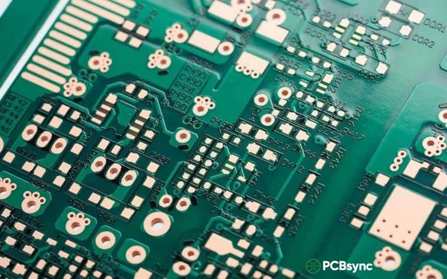
After 15 years designing PCBs for everything from industrial control systems to aerospace equipment, I can tell you that choosing the right surface finish makes or breaks your product. Hard gold plating PCB technology remains one of the most misunderstood yet critical decisions engineers face today.
I’ve seen too many projects fail because someone chose ENIG where hard gold was needed, or wasted budget on full-body hard gold when selective plating would suffice. The difference between a connector that lasts 10 years and one that fails after six months often comes down to surface finish selection. This guide cuts through the confusion and gives you practical knowledge based on real manufacturing experience.
Whether you’re designing edge connectors for server backplanes, keypads for medical equipment, or gold fingers for memory modules, understanding hard gold plating PCB specifications will save you time, money, and headaches down the road. We’ll cover everything from thickness standards and IPC specifications to real-world design guidelines that prevent manufacturing problems.
Hard gold plating PCB (also called electrolytic hard gold) is a surface finish where gold alloyed with cobalt or nickel is electroplated onto specific areas of a printed circuit board. The “hard” designation comes from adding 0.1-0.3% cobalt or nickel to the gold, which increases hardness from about 60-90 HK (Knoop Hardness) for pure gold to 130-200 HK for hard gold.
The process deposits gold over a nickel barrier layer using electrochemical deposition. Unlike ENIG (Electroless Nickel Immersion Gold), which relies on chemical displacement reactions, hard gold plating requires electrical current flowing through the PCB to build up the gold layer. This fundamental difference explains why hard gold plating PCB must be applied before solder mask—the plating bath needs electrical connectivity to the areas being plated.
Here’s what makes hard gold plating PCB unique: the electroplating process creates a denser crystal structure compared to immersion gold. This density, combined with the alloying elements, gives hard gold its characteristic wear resistance. At 30 microinches thickness, properly plated hard gold can survive over 1,000 insertion cycles before showing significant wear.
Hard Gold Plating PCB Calculator
PCBSync Engineering Tools
Gold Plating Area Dimensions
mm
mm
pcs
pcs
Gold Thickness Selection
50 cycles2505007501000 cycles
Calculation Results
—
Total Plating Area (mm²)
—
Gold Volume (mm³)
—
Gold Weight (mg)
—
Nickel Weight (mg)
—
Recommended Thickness
—
Expected Hardness (HV)
💡 Design Recommendation
Based on your insertion cycle requirements, the recommended gold thickness ensures optimal wear resistance and electrical performance for your application.
Cost Parameters
$/gram
cm²
cm²
pcs
Additional Options
Cost Breakdown
Gold Material Cost$0.00
Nickel Plating Cost$0.00
Process & Labor Cost$0.00
Additional Options$0.00
Estimated Total$0.00
💰 Cost Optimization Tips
• Minimize gold finger area where possible
• Consider ENIG for areas not requiring insertion wear resistance
• Order in larger quantities for volume discounts
• Standard thicknesses (30-50 μ”) are more cost-effective
Design Note: Hard gold areas should be kept separate from ENIG/ENEPIG surface finish areas. Use solder mask to define boundaries clearly. Ensure adequate clearance from solder joints.
Hard gold plating PCB comes in two main application types: full-body and selective. Full-body hard gold covers the entire PCB surface, which is expensive and rarely necessary. Selective hard gold (also called localized gold plating) applies gold only to specific areas that need it—typically edge connectors, keypads, or contact points.
Most applications use selective hard gold plating to optimize cost. For instance, a memory module only needs hard gold on the edge connector fingers, not the entire board. The rest of the board can use ENIG, OSP, or immersion silver for the solderable areas. This combination approach—hard gold where you need wear resistance, and a solderable finish everywhere else—gives you the best of both worlds.
Hard Gold vs Soft Gold vs ENIG: Key Differences
One of the most common questions I get from junior engineers is about the differences between gold finish options. The terminology gets confusing because “gold plating” can mean several different things depending on context. Let me break this down clearly so you can make informed decisions.
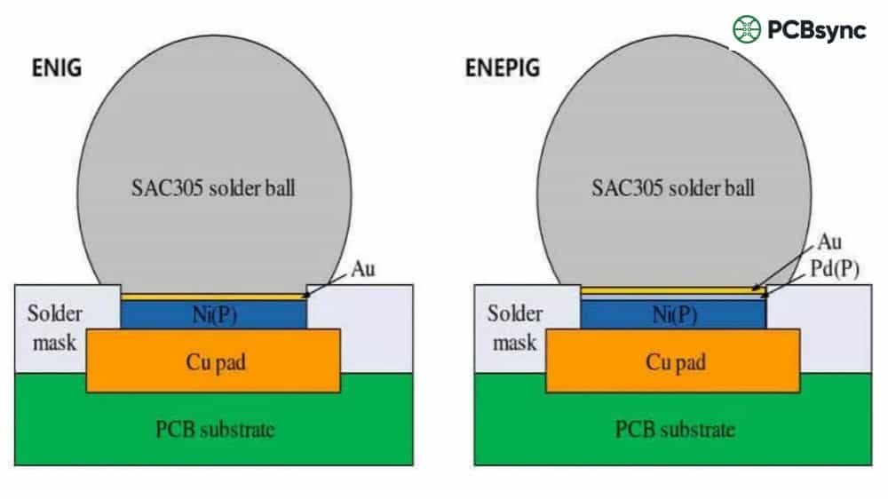
The fundamental distinction comes down to purity and process. Hard gold contains alloying elements (cobalt or nickel) and is electroplated. Soft gold is pure (99.9%) and can be either electroplated or chemically deposited. ENIG uses chemical deposition and produces a thin pure gold layer. Each serves different purposes and shouldn’t be used interchangeably.
Property
Hard Gold
Soft Gold
ENIG
Gold Purity
99.7% (with Co/Ni)
99.9% pure
99.9% pure
Thickness Range
3-50 μin (0.08-1.27 μm)
10-50 μin (0.25-1.27 μm)
2-5 μin (0.05-0.13 μm)
Hardness (HK)
130-200 HK
60-90 HK
60-90 HK
Solderability
Poor
Excellent
Excellent
Wear Resistance
Excellent
Moderate
Poor
Wire Bonding
Not suitable
Excellent
Good (limited)
Relative Cost
High
Highest
Moderate
Primary Use
Edge connectors, keypads
Wire bonding (COB)
SMT pads, BGA
The appearance also differs noticeably. Hard gold plating PCB surfaces appear slightly whitish or pale yellow due to the nickel or cobalt content, while ENIG has a brighter, more golden appearance. This visual difference actually helps during inspection—you can often spot which finish was used just by looking at the board.
Understanding the manufacturing process helps you design better boards and communicate effectively with your fabricator. Here’s how hard gold plating PCB production actually works:
Surface Preparation: The copper surface gets thoroughly cleaned using acid washing and micro-etching. Any contamination—oils, oxides, or residues—will cause adhesion failures. Most shops use sulfuric acid followed by thorough water rinses.
Masking: Blue adhesive tape or photoresist covers all areas except those requiring gold plating. For edge connectors, only the finger pads remain exposed. This selective approach keeps costs down—gold is expensive.
Nickel Underplating: A nickel barrier layer (typically 3-6 μm or 120-240 μin) gets electroplated onto the copper. This nickel serves three critical functions: it prevents copper-gold interdiffusion, provides mechanical support, and acts as a barrier against corrosion.
Hard Gold Electroplating: The PCB enters the gold plating bath containing potassium gold cyanide (K[Au(CN)₂]) along with cobalt or nickel salts. Electrical current deposits the gold-alloy layer onto the nickel surface. Plating time and current density control the final thickness.
Rinsing and Gold Recovery: Multiple deionized water rinses remove plating solution residues. Excess gold gets recovered from the rinse water—this isn’t just environmental responsibility, it’s economics.
Quality Verification: X-ray fluorescence (XRF) measures gold and nickel thickness. Visual inspection under magnification checks for defects. Tape adhesion tests verify the plating won’t peel under mechanical stress.
Important note: The gold plating must happen before solder mask application. This process sequence is non-negotiable because electroplating requires electrical connectivity to the areas being plated. Planning your manufacturing sequence correctly from the start prevents costly redesigns and schedule delays.
Hard Gold Plating PCB Thickness Standards and Specifications
Thickness specifications vary based on application requirements and industry standards. Getting this right matters—too thin and you’ll have premature wear, too thick and you’re wasting money.
IPC Standards for Hard Gold Plating
IPC-4556 specifically addresses gold finger requirements. According to this standard, the typical gold finger thickness is 30-32 μin (approximately 0.76-0.81 μm), with acceptable ranges from 3-50 μin depending on application requirements.
Application Type
Gold Thickness
Nickel Thickness
IPC Class 1 & 2 (Commercial)
≥25 μin (0.64 μm)
≥100 μin (2.54 μm)
IPC Class 3 (High Reliability)
≥50 μin (1.27 μm)
≥100 μin (2.54 μm)
Military (MIL-G-45204)
50-100 μin (1.27-2.54 μm)
≥150 μin (3.81 μm)
High-Wear Industrial
Up to 150 μin (3.81 μm)
≥200 μin (5.08 μm)
Standard Gold Fingers
30-32 μin (0.76-0.81 μm)
≥120 μin (3.05 μm)
The IPC-6012 standard covers general PCB qualification including hard gold plating requirements. For most commercial applications, 30 μin of hard gold over 100 μin of nickel provides adequate durability for approximately 1,000 insertion cycles.
When calculating your requirements, consider the expected product lifetime and usage frequency. A server component that gets swapped once a year needs far less wear resistance than a diagnostic tool connector used dozens of times daily. I generally recommend specifying 20-30% more thickness than the minimum calculated requirement to provide safety margin against manufacturing variations.
Applications of Hard Gold Plating PCB
Hard gold plating PCB finds its way into products where reliability and durability justify the cost premium. Here are the primary applications I’ve worked with over the years:
Edge Connectors and Gold Fingers
This is where hard gold plating PCB truly shines. RAM modules, graphics cards, PCI Express cards, and server expansion boards all use gold fingers for their slot connections. The repeated insertion and removal cycles demand hard gold’s wear resistance. You’ll find gold fingers on virtually every computer motherboard’s expansion slots.
I recently worked on a project for data center equipment where the boards would be hot-swapped hundreds of times over their service life. Standard ENIG would have failed within months. We specified 50 μin hard gold and the connectors are still performing perfectly after two years of field deployment. The extra cost was less than 10% of total board cost—trivial compared to the value of reliable operation.
Keypads and Membrane Switches
Industrial control panels, medical device interfaces, and point-of-sale terminals often use hard gold plated contact pads. These applications involve millions of key presses over the product lifetime. The contact points need to maintain consistent electrical characteristics despite constant mechanical stress.
Selective hard gold plating works well here—you plate only the actual contact areas while using standard finishes elsewhere. This keeps costs reasonable while providing the durability where it matters. Some designs use different gold thicknesses for different keys based on expected usage frequency.
Aerospace, Military, and Medical Equipment
High-reliability applications in these industries demand hard gold plating PCB for connector interfaces. Satellite communication systems, radar equipment, avionics, implantable medical devices, and diagnostic equipment all benefit from hard gold’s corrosion resistance and long-term reliability.
These sectors typically specify MIL-G-45204 compliance, requiring thicker gold deposits (50-100 μin) and stricter quality controls. The cost premium is negligible compared to the consequences of field failures. When a satellite in orbit or a cardiac pacemaker in a patient needs to work reliably for years without maintenance, hard gold provides the assurance these applications demand.
Medical device manufacturers particularly value hard gold plating PCB for equipment that gets sterilized repeatedly. The finish withstands autoclave cycles and chemical sterilization processes that would degrade other surface finishes. I’ve seen hard gold connectors on endoscopic equipment maintain perfect electrical characteristics after thousands of sterilization cycles.
Test Equipment and Burn-In Boards
Test fixtures and burn-in boards see thousands of connections during their service life. Hard gold plated test points and ZIF (Zero Insertion Force) connector pads maintain reliable contact through extensive use cycles.
Benefits of Hard Gold Plating PCB
Superior Wear Resistance: At 130-200 HK hardness, hard gold withstands mechanical abrasion far better than soft gold or ENIG. This translates directly to longer service life for connector applications.
Excellent Electrical Conductivity: Gold maintains low and stable contact resistance over time. Unlike other metals, it doesn’t form resistive oxide layers, ensuring consistent signal integrity throughout the product lifetime.
Corrosion and Oxidation Resistance: Gold is virtually inert. Hard gold plating PCB surfaces won’t degrade in storage or challenging operating environments, giving you excellent shelf life and long-term reliability.
RoHS Compliance: Hard gold plating is lead-free and fully compliant with RoHS and REACH regulations. No special handling or documentation headaches.
Proven Track Record: This technology has decades of successful field deployment. You’re not experimenting with something new—hard gold plating PCB is a mature, well-understood process.
Limitations and Considerations
Hard gold plating PCB isn’t the right choice for every application. Understanding the limitations helps you make better design decisions:
Poor Solderability: The cobalt or nickel alloying elements oxidize at soldering temperatures, reducing solder joint strength. Never use hard gold on SMT pads—it’s not designed for soldering.
Higher Cost: Gold is expensive, and the electroplating process adds manufacturing complexity. Only specify hard gold where the application truly requires it. As a rough guideline, hard gold plating can add 15-30% to your board cost depending on the plated area and thickness requirements.
Design Constraints: The electroplating process requires electrical connectivity to plated areas during pcb manufacturing. This constrains PCB layout and panelization options.
Limited Manufacturer Availability: Not all PCB shops offer hard gold plating. The process requires specialized equipment, gold salt handling permits, and wastewater treatment capabilities.
Design Guidelines for Hard Gold Plating PCB
Following these design rules will help ensure successful manufacturing and optimal performance. I’ve compiled these based on years of working with PCB fabricators and debugging manufacturing issues. Most problems with hard gold plating PCB trace back to design violations:
Gold Finger Placement: Position gold fingers on the PCB edge, facing outward from the panel center. This allows proper electrical connection during plating and easy beveling afterward. The finger pads need to connect to the panel frame for electroplating—this connection gets removed during depaneling.
Clearance from PTH: Maintain at least 1.0 mm (40 mil) distance between gold fingers and any plated through-holes. This prevents plating solution contamination and ensures clean finger surfaces. Some manufacturers require 2.0 mm for optimal results.
Solder Mask Clearance: Keep solder mask and silkscreen at least 1.0 mm away from gold-plated areas. Any overlap can cause contamination or adhesion problems.
Inner Layer Copper: Remove copper from inner layers at the PCB edge where gold fingers are located. Copper exposure during beveling creates contamination issues and can damage the bevel machine.
Plating Traces: Connect all gold finger pads with a thin conductor trace (typically 0.2 mm / 8 mil) at the panel edge for electroplating. This trace gets removed during depaneling or beveling.
Beveling Specifications: Standard bevel angles are 30° or 45°, with 45° being most common. Specify bevel depth based on your connector requirements—typically this matches the PCB thickness minus a small margin.
Maximum Pad Length: Gold finger pads should not exceed 40 mm in length. Standard shallow plating baths have depth limitations.
Quick Reference: Design Rules
Parameter
Requirement
Distance from PTH
≥1.0 mm (40 mil)
Solder mask clearance
≥1.0 mm (40 mil)
Distance from board edge
≥0.5 mm (20 mil)
Maximum finger length
40 mm
Typical finger width
1.0-3.5 mm
Standard bevel angle
30° or 45°
Plating trace width
≥0.2 mm (8 mil)
Quality Control and Testing for Hard Gold Plating PCB
When you receive hard gold plated PCBs from your manufacturer, here’s what to verify:
Visual Inspection: Check for uniform color (slightly pale gold/white-gold appearance), smooth surface without pitting or nodules, and no contamination or staining. Use 10x magnification for detailed inspection per IPC-A-600 guidelines.
Thickness Verification: Request XRF (X-ray fluorescence) measurement reports showing both gold and nickel thickness. Verify values meet your specifications and IPC class requirements.
Adhesion Testing: The tape test (per IPC-TM-650 method 2.4.1) should show no peeling or flaking when adhesive tape is pressed firmly onto the gold surface and then removed.
Hardness Testing: For critical applications, request microhardness testing. Hard gold should measure 130-200 HK (Knoop Hardness). Values below 130 HK indicate insufficient hardener content.
Reputable PCB manufacturers provide test reports and certificates of compliance with your orders. If your supplier doesn’t offer this documentation automatically, request it. For military and aerospace applications, full traceability documentation is mandatory.
Useful Resources and References
Here are the standards and resources I reference regularly when working with hard gold plating PCB designs. These documents provide the technical specifications you need for proper design and quality verification:
IPC-4556: Specification for Electroless Nickel/Electroless Palladium/Immersion Gold (ENEPIG) and Electroless Nickel/Immersion Gold (ENIG) Plating for Printed Circuit Boards – IPC Standards
IPC-6012: Qualification and Performance Specification for Rigid Printed Boards – IPC Standards
MIL-G-45204: Gold Plating, Electrodeposited (Military Standard) – Available through ASSIST database
IPC-A-600: Acceptability of Printed Boards – Visual inspection criteria including gold plating
ASTM B488: Standard Specification for Electrodeposited Coatings of Gold for Engineering Uses
Frequently Asked Questions
What is the difference between hard gold and ENIG?
Hard gold is electroplated gold alloyed with cobalt or nickel, making it harder and more wear-resistant. It’s applied before solder mask and used for mechanical contact areas like connectors and keypads. ENIG (Electroless Nickel Immersion Gold) is chemically deposited pure gold over nickel, applied after solder mask, and designed primarily for soldering applications. Hard gold is significantly thicker (30-50 μin typical) while ENIG is thin (2-5 μin). The key decision point: choose hard gold for connectors and areas requiring wear resistance; choose ENIG for SMT pads and solderable surfaces.
How thick should gold fingers be?
According to IPC-4556, the standard thickness for gold fingers is 30-32 μin (0.76-0.81 μm). For commercial applications (IPC Class 1 & 2), minimum 25 μin is acceptable. High-reliability applications (IPC Class 3) require minimum 50 μin. Military and aerospace applications typically specify 50-100 μin per MIL-G-45204. The underlying nickel should be at least 100-150 μin thick. When specifying thickness, consider the expected number of insertion cycles—thicker gold lasts longer but costs more.
Can hard gold be soldered?
Technically yes, but it’s not recommended and should be avoided in production designs. The cobalt or nickel alloying elements in hard gold oxidize at soldering temperatures, weakening solder joints and potentially causing reliability issues. If you must solder to hard gold surfaces in a prototype or repair situation, use highly active flux and expect reduced joint strength compared to proper solderable finishes. For production boards, always specify ENIG, immersion silver, OSP, or HASL for solderable areas.
Is hard gold plating RoHS compliant?
Yes, hard gold plating is fully RoHS and REACH compliant. Gold, nickel, and cobalt are not restricted substances under these regulations. Hard gold plating PCB contains no lead or other hazardous materials, making it suitable for all markets including the European Union. This makes hard gold an excellent choice for applications transitioning from older lead-based finishes. Always verify compliance documentation with your PCB manufacturer and request certificates of compliance for your records.
How many insertion cycles can hard gold fingers withstand?
At standard 30 μin thickness, properly plated hard gold fingers typically survive 500-1,000 insertion cycles before showing significant wear. Increasing thickness to 50 μin extends this to 1,000-2,000 cycles. For applications requiring more cycles, specify thicker gold (up to 100-150 μin for extreme durability requirements). The nickel underlayer thickness also affects durability—thicker nickel provides better mechanical support and acts as a more effective diffusion barrier. Environmental factors like humidity and contamination can reduce cycle life, so consider your operating environment when specifying thickness.
Conclusion
Hard gold plating PCB remains the gold standard (pun intended) for connector applications requiring durability and reliability. While it costs more than alternative finishes, the performance benefits justify the investment for edge connectors, keypads, test fixtures, and high-reliability applications in aerospace, military, and medical industries.
The key takeaways from this guide: specify hard gold only where you need wear resistance, follow IPC thickness guidelines for your application class, and work with experienced manufacturers who understand the process requirements. Don’t over-engineer with full-body hard gold when selective plating will do, but don’t cut corners on thickness for critical applications where connector failure isn’t an option.
Remember the design fundamentals: maintain proper clearances from plated through-holes and solder mask, keep inner layers copper-free at the PCB edge, and specify appropriate bevel angles for your connectors. These seemingly small details prevent big problems during manufacturing and field deployment.
If you’re still uncertain about whether hard gold plating PCB is right for your project, reach out to your PCB manufacturer early in the design process. A good fab shop can provide guidance on specifications, help optimize your design for manufacturability, and ensure you get the reliability you need without overspending. The best time to discuss surface finish requirements is before you finalize your design—not when you’re troubleshooting field failures.
Inquire: Call 0086-755-23203480, or reach out via the form below/your sales contact to discuss our design, manufacturing, and assembly capabilities.
Quote: Email your PCB files to Sales@pcbsync.com (Preferred for large files) or submit online. We will contact you promptly. Please ensure your email is correct.
Notes: For PCB fabrication, we require PCB design file in Gerber RS-274X format (most preferred), *.PCB/DDB (Protel, inform your program version) format or *.BRD (Eagle) format. For PCB assembly, we require PCB design file in above mentioned format, drilling file and BOM. Click to download BOM template To avoid file missing, please include all files into one folder and compress it into .zip or .rar format.


