Inquire: Call 0086-755-23203480, or reach out via the form below/your sales contact to discuss our design, manufacturing, and assembly capabilities.
Quote: Email your PCB files to Sales@pcbsync.com (Preferred for large files) or submit online. We will contact you promptly. Please ensure your email is correct.
Notes: For PCB fabrication, we require PCB design file in Gerber RS-274X format (most preferred), *.PCB/DDB (Protel, inform your program version) format or *.BRD (Eagle) format. For PCB assembly, we require PCB design file in above mentioned format, drilling file and BOM. Click to download BOM template To avoid file missing, please include all files into one folder and compress it into .zip or .rar format.
If you’ve been working in PCB design or procurement for any length of time, you’ve undoubtedly noticed the growing emphasis on halogen-free materials throughout the electronics industry. This isn’t just another fleeting trend or marketing buzzword—there are substantial engineering, environmental, and regulatory reasons driving this fundamental shift in how circuit boards are manufactured. Having worked on hundreds of board designs across automotive, medical, and consumer electronics applications over the years, I’ve witnessed firsthand how material choices directly impact everything from thermal reliability to manufacturability to end-of-life disposal compliance.
In this comprehensive guide, I’ll walk you through exactly what halogen free PCB actually means in practical terms, break down the international standards you absolutely need to understand, and explain why this topic should matter for your next project. Whether you’re designing mission-critical systems for automotive applications, precision medical devices, high-volume consumer electronics, or rugged industrial equipment, understanding halogen-free requirements has become essential foundational knowledge for any serious PCB engineer or procurement specialist.
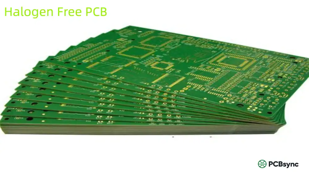
A halogen free PCB is a printed circuit board manufactured using substrate materials, solder masks, and other components that contain extremely low levels of halogen elements—specifically chlorine (Cl) and bromine (Br). These boards utilize alternative flame retardant systems based primarily on phosphorus compounds, nitrogen-based chemicals, or metal hydroxides instead of the traditional brominated flame retardants that have been industry standard for decades.
But let’s establish some precision here, because the term “halogen-free” doesn’t actually mean zero halogens present. In reality, achieving absolutely zero halogen content would be practically impossible and economically prohibitive. According to the most widely recognized and internationally accepted industry standards—specifically IEC 61249-2-21 and JPCA-ES-01-2003—a PCB qualifies as halogen-free when it meets these specific threshold requirements:
Chlorine (Cl): Less than 900 ppm (0.09% by weight)
Bromine (Br): Less than 900 ppm (0.09% by weight)
Combined Cl + Br: Less than 1500 ppm (0.15% by weight)
These threshold values aren’t arbitrary numbers pulled from thin air—they represent carefully determined detection limits that testing laboratories around the world can reliably and repeatably measure using standardized analytical methods. The primary test methodology involves oxygen bomb combustion to convert all halogen compounds (both ionic and covalently bonded) into halide ions, followed by ion chromatography analysis to quantify the exact concentrations present.
Understanding Halogens in Electronics Manufacturing
The halogens are Group 17 elements in the periodic table, consisting of fluorine (F), chlorine (Cl), bromine (Br), iodine (I), and astatine (At). In the PCB manufacturing world, engineers are primarily concerned with chlorine and bromine because these two elements have historically been the most commonly used in flame retardant compounds and various processing chemicals throughout the PCB fabrication process.
For several decades, brominated flame retardants—particularly tetrabromobisphenol A (TBBPA)—served as the go-to solution for making FR4 laminates meet fire resistance requirements. These compounds are chemically effective at interrupting combustion reactions, relatively inexpensive to manufacture and incorporate, and don’t significantly degrade the electrical properties of the base laminate material. The fundamental problem arises when these halogenated materials are exposed to high temperatures during combustion or improper disposal. Under these conditions, they release highly toxic compounds including hydrogen bromide (HBr) gas, polybrominated dibenzo-p-dioxins (PBDDs), and polybrominated dibenzofurans (PBDFs)—all of which pose serious risks to human health and the environment.
The situation becomes particularly concerning during e-waste processing. When circuit boards containing brominated flame retardants are improperly incinerated—a disturbingly common practice in many parts of the world—the resulting toxic emissions can contaminate air, soil, and water supplies, creating long-term environmental and public health problems that persist for generations.
International Standards for Halogen Free PCB Materials
One of the more frustrating challenges I’ve encountered when specifying halogen-free materials for projects is navigating the various overlapping standards from different organizations. Multiple industry bodies have established their own definitions and test methods, and while these standards are largely aligned in their fundamental approach, there are important nuances that engineers and procurement specialists must understand to avoid costly mistakes.
Standard
Halogen Limits
Scope of Application
IEC 61249-2-21
Cl <900ppm, Br <900ppm, Total <1500ppm
PCB laminates and base materials
JPCA-ES-01-2003
Cl <900ppm, Br <900ppm, Total <1500ppm
Copper-clad laminates (Japan standard)
IPC-4101B
Cl <900ppm, Br <900ppm, Total <1500ppm
Laminate/prepreg material specs
JEDEC JS709C
Br <1000ppm (BFR), Cl <1000ppm (CFR/PVC)
Solid-state devices and components
IPC J-STD-004C
Varies by flux type classification
Soldering fluxes and solder pastes
Critical Distinction: Don’t confuse “halogen-free” with “halide-free”—these terms have different technical meanings. Halides are ionic forms of halogens (like chloride ions commonly found in flux residues) and are measured using different analytical techniques. A soldering flux can be classified as halide-free while still containing covalently bonded halogens in its chemical formulation, or vice versa. Always verify which specific standard and test method applies to your particular application requirements before making procurement decisions.
Why Halogen Free PCB Matters for Your Projects
The industry-wide shift toward halogen-free electronics isn’t simply about checking a compliance box on a form or satisfying environmental activists. There are legitimate, measurable technical advantages, environmental benefits, and compelling business reasons driving broad adoption across virtually every electronics sector.
Environmental and Health Considerations
When traditional brominated PCBs undergo combustion—whether in an accidental fire incident or during end-of-life disposal at waste processing facilities—they release a toxic cocktail of dangerous compounds. Hydrogen bromide gas is highly corrosive and acutely toxic to respiratory systems. The dioxins and furans formed during incomplete combustion are classified as persistent organic pollutants (POPs) that bioaccumulate progressively up the food chain, concentrating in fatty tissues of animals and humans. These environmental and health concerns aren’t theoretical speculation—they’re well-documented through decades of peer-reviewed scientific literature and real-world contamination incidents.
The European Union’s landmark RoHS (Restriction of Hazardous Substances) directive specifically prohibited polybrominated biphenyls (PBB) and polybrominated diphenyl ethers (PBDE) effective July 2006. While TBBPA—the most commonly used brominated flame retardant in PCB laminates—wasn’t included in that initial restricted substances list, the clear regulatory trajectory points toward increasingly strict limitations on all halogenated compounds in electronics manufacturing.
Regulatory Compliance and Global Market Access
Multiple major OEMs now mandate halogen-free materials throughout their entire supply chains as a condition of doing business. Global technology leaders including Apple, Samsung, Sony, Dell, HP, and numerous automotive manufacturers have made public corporate commitments to systematically phase out halogenated flame retardants from their products. If you’re positioning your company to supply components or assemblies to these organizations, halogen-free compliance isn’t an optional nice-to-have feature—it’s a fundamental qualification requirement that determines whether you can even participate in the bidding process.
RoHS (Restriction of Hazardous Substances): Explicitly restricts PBB and PBDE brominated flame retardants in electronics sold in EU markets
WEEE (Waste Electrical and Electronic Equipment): Encourages use of recyclable materials and proper end-of-life disposal practices
REACH (Registration, Evaluation, Authorization of Chemicals): Mandates disclosure and authorization for substances of very high concern
California Proposition 65: Requires consumer warning labels for products containing known carcinogens or reproductive toxins
Technical Advantages of Halogen Free Materials
Here’s something that genuinely surprised me when I first started extensively working with halogen-free laminate materials: they frequently perform measurably better than traditional FR4 across several important performance parameters. The phosphorus and nitrogen-based flame retardant chemical systems used in halogen-free laminates can actually deliver meaningful improvements in board performance and reliability.
Performance Property
Standard FR4
Halogen Free FR4
Glass Transition Temp (Tg)
130-140°C
150-180°C
Decomposition Temp (Td)
310-320°C
330-350°C
CTE (Z-axis expansion)
Higher expansion
Lower (improved)
Moisture Absorption
0.10-0.15%
<0.10%
Insulation Resistance
Standard
Improved (lower polarity)
Dielectric Constant (Dk)
~4.5
~4.2-4.4 (lower)
Material Cost Premium
Baseline reference
+10-30% typical
The significantly higher Tg and lower coefficient of thermal expansion (CTE) values of halogen-free materials make them particularly well-suited for lead-free assembly processes, which require substantially higher reflow temperatures (typically peaking around 260°C) than traditional tin-lead soldering. The improved moisture resistance characteristics also enhance long-term reliability performance in humid operating environments—something I’ve seen make a tangible difference in field failure rates for automotive and industrial control applications.
The major laminate manufacturers have invested heavily in developing halogen-free alternatives that match or exceed the performance characteristics of traditional brominated materials. The technology has matured considerably over the past decade, and today’s halogen-free laminates offer excellent reliability and processability. Here are some of the most commonly specified options you’ll encounter:
Popular Halogen Free Laminates by Manufacturer
Material Grade
Manufacturer
Tg (°C)
Td (°C)
Primary Applications
S1165 / S1165M
ShengYi
150-170
330
Consumer electronics, mobile
R1566 / R1566W
Panasonic
170
340
Automotive, industrial control
IT-170GRA1TC / IT-170GLE
ITEQ
170
340
High-layer count, HDI PCBs
DE156 / GreenSpeed
Isola
150
340
General purpose HF
VT-447 / VT-481
Ventec
170
340
LED, power electronics
TU883 / TU862HF
TUC
175
340
High-frequency, RF applications
Alternative Flame Retardant Chemical Systems
Halogen-free laminates achieve the required UL94 V-0 fire resistance rating through fundamentally different chemical mechanisms than traditional brominated systems. Understanding these mechanisms helps engineers appreciate why halogen-free materials often exhibit different processing characteristics:
Phosphorus-Based Compounds: When exposed to heat, these compounds thermally decompose to form polyphosphoric acid, which creates a protective carbonaceous char layer on the material surface. This char layer physically insulates the underlying substrate from heat while simultaneously limiting oxygen access to the combustion zone.
Nitrogen-Based Compounds: Release non-flammable nitrogen gases during thermal decomposition that dilute combustible vapors in the immediate flame zone, effectively smothering the fire by reducing the concentration of flammable gases below the combustion threshold.
Phosphorus-Nitrogen Synergistic Systems: Combine both mechanisms for enhanced fire resistance with better overall performance. These dual-action systems are particularly common in demanding automotive and industrial control applications where reliability is paramount.
Metal Hydroxides (ATH/MDH): Release water vapor endothermically when heated, simultaneously cooling the material and diluting flammable gases. Aluminum trihydrate and magnesium dihydroxide are the most common examples used in electronics applications.
Key Applications for Halogen Free PCB Technology
Halogen-free PCBs have evolved from specialized niche applications to mainstream use across virtually every sector of the electronics industry. Here’s where these materials are most commonly specified and why:
Automotive Electronics and Electric Vehicles
The automotive industry has been a major driving force behind halogen-free adoption. Electric vehicle battery management systems (BMS), advanced driver assistance system (ADAS) sensors, infotainment head units, engine control modules (ECUs), and inverter power electronics all benefit significantly from the enhanced thermal stability and improved long-term reliability characteristics of halogen-free materials. The demanding operating environment—with wide temperature cycling ranges, mechanical vibration, and extended service life requirements—makes these enhanced material properties particularly valuable. Major automotive OEMs including BMW, Mercedes-Benz, Toyota, and Tesla have implemented halogen-free requirements across their supply chains.
Medical Devices and Healthcare Equipment
Medical equipment represents perhaps the most safety-critical application space, requiring materials that won’t release any toxic substances under any conceivable circumstances during the product lifecycle. Diagnostic imaging equipment, patient monitoring systems, surgical instruments, implantable devices, and wearable health monitoring products increasingly specify halogen-free PCBs. Beyond regulatory compliance considerations, there’s a compelling ethical argument for minimizing potentially harmful materials in products that directly contact patients or operate in clinical environments.
Consumer Electronics and Mobile Devices
Smartphones, tablets, laptops, smartwatches, and wireless earbuds are now routinely manufactured using halogen-free circuit boards. Global technology brands including Apple, Samsung, Google, Microsoft, and Amazon have made public commitments to eliminate brominated flame retardants from their entire product portfolios. This isn’t merely marketing positioning—it reflects genuine consumer demand for environmentally responsible products and the brands’ recognition that sustainability initiatives positively impact purchasing decisions.
Telecommunications and 5G Network Infrastructure
High-frequency applications like 5G base station equipment, RF power amplifiers, and networking infrastructure benefit substantially from the electrical characteristics of halogen-free materials. The typically lower dielectric constant (Dk) and reduced dissipation factor (Df) values can improve signal integrity and reduce losses at higher frequencies where these parameters become increasingly critical. Additionally, telecom equipment often operates continuously in enclosed indoor spaces, making the dramatically reduced smoke and toxic emission profile during potential fire events particularly attractive from workplace safety and insurance liability perspectives.
Industrial Control, Aerospace, and Renewable Energy
Industrial automation controllers, robotics systems, aerospace avionics, satellite communication equipment, solar inverters, and wind turbine control systems all represent growing markets for halogen-free PCB materials. These applications typically demand exceptional long-term reliability, resistance to harsh environmental conditions, and compliance with industry-specific safety certifications that increasingly favor or mandate halogen-free materials.
Testing Methods for Verifying Halogen Content
Verifying halogen-free compliance requires specific, validated analytical test methods. The most reliable and widely accepted approach combines proper sample preparation with sensitive analytical detection:
Oxygen Bomb Combustion (EN 14582): The sample is completely combusted in a sealed, pressurized oxygen-filled flask. This process converts all halogen atoms—both ionic and covalently bonded forms—into halide ions that can be subsequently measured. This sample preparation step is critical for accurate total halogen determination.
Ion Chromatography (IPC-TM-650 2.3.28): The combustion products dissolved in absorption solution are analyzed using ion chromatography to precisely quantify chloride, bromide, fluoride, and other halide ions present. The separation and detection capabilities of modern IC systems provide excellent sensitivity and specificity.
XRF Screening (X-Ray Fluorescence): Provides rapid non-destructive screening for halogen elements, useful for incoming inspection of materials. However, XRF is less precise than combustion/IC methods and may not accurately quantify borderline samples near threshold limits.
Engineer’s Pro Tip: When requesting test reports and compliance certificates from your laminate supplier, always verify they’re using oxygen bomb combustion followed by ion chromatography analysis. Simpler extraction-based methods may miss covalently bonded halogens that would still be released during actual thermal events like fires or reflow soldering.
Practical Design and Manufacturing Considerations
Transitioning from traditional FR4 to halogen-free materials isn’t always a simple drop-in substitution. Based on my practical project experience, here are the key technical considerations to address:
Drilling Process Parameters: Halogen-free laminates tend to be harder and more abrasive to tooling than standard FR4. Expect approximately 20-25% reduction in carbide drill bit life. Consider adjusting spindle speeds and feed rates, and evaluate specialized drill geometries designed for harder materials in high-volume production scenarios.
Moisture Sensitivity Management: While halogen-free materials generally exhibit lower steady-state moisture absorption, some specific formulations may require extended pre-assembly baking times to ensure optimal soldering results. Always follow the laminate manufacturer’s specific recommendations for your chosen material grade.
Solder Mask Material Compatibility: Ensure your specified solder mask is also halogen-free compliant. Using a halogen-free laminate substrate with a conventional halogenated solder mask defeats the environmental purpose and may cause compliance issues with your end customer’s requirements.
Lead-Free Assembly Compatibility: The inherently higher Tg of most halogen-free materials makes them naturally well-suited for lead-free soldering temperature profiles (typically requiring 260°C peak temperatures). This represents a genuine advantage over standard FR4 for lead-free processes.
Cost and Budget Planning: Budget appropriately for a 10-30% material cost premium compared to equivalent standard FR4 grades. However, remember to evaluate total cost of ownership—improved field reliability, reduced warranty claims, and streamlined regulatory compliance may more than offset the higher initial material investment over the product lifecycle.
Useful Technical Resources and Reference Links
Here are authoritative resources I’ve found consistently valuable when working with halogen-free specifications and material selection:
International Standards and Specifications:
IEC 61249-2-21 – Primary international halogen-free definition standard for PCB laminates
IPC-4101B – Comprehensive base materials specifications including halogen-free laminate designations
JEDEC JS709C – Low-halogen definition standard for complete electronic products and components
IPC-TM-650 2.3.28 – Ion chromatography test method for halide/halogen content determination
IPC J-STD-004C – Requirements for soldering fluxes including halide activity classification
Technical Reference and Research Sites:
CALCE (University of Maryland) – calce.umd.edu/halogen-free-electronics – Academic research resource
RoHS Guide – rohsguide.com – Comprehensive regulatory compliance information
IPC.org – Official source for industry standards and test method documentation
No, these are distinct and separate requirements. RoHS (Restriction of Hazardous Substances) restricts specific listed substances including lead, mercury, cadmium, hexavalent chromium, PBB, and PBDE. A PCB can be fully RoHS compliant while still containing substantial amounts of halogens (such as TBBPA-based flame retardants) that aren’t on the RoHS restricted list. Halogen-free is a stricter, additional requirement that addresses a different set of environmental and health concerns.
Is standard FR4 material halogen-free?
No. Conventional standard FR4 laminate typically uses brominated flame retardants (usually TBBPA incorporated into the epoxy resin) to achieve the required UL94 V-0 flammability rating. To get halogen-free performance, you must specifically request halogen-free FR4 variants—such as those listed in the materials table in this article—from your laminate supplier or PCB manufacturer.
Are there legal requirements mandating halogen-free PCBs?
Currently, no major jurisdiction has enacted laws legally mandating halogen-free PCBs across all product categories. However, market forces and major OEM purchasing requirements have made halogen-free materials effectively mandatory in automotive, consumer electronics, and other major sectors. The clear regulatory trajectory points toward increasingly strict restrictions on halogenated compounds, making early adoption a prudent strategy for future-proofing your products and supply chain.
What’s the typical cost difference for halogen-free PCBs?
Expect a 10-30% premium on raw material costs depending on the specific laminate grade selected and your order volume. Manufacturing processing costs may also be marginally higher due to adjusted drilling parameters and potentially slower production rates. However, as global demand for halogen-free materials continues to increase and production volumes scale up, the cost gap compared to standard materials has been steadily narrowing over recent years.
Can halogen-free PCBs handle lead-free soldering processes?
Yes—and they’re actually better suited for lead-free assembly than standard FR4 in most cases. The significantly higher glass transition temperature (typically 150-180°C versus 130-140°C for standard FR4) means halogen-free laminates can more easily withstand the elevated reflow temperatures required for lead-free solder alloys (typically peaking around 260°C) without experiencing thermal degradation, delamination, or excessive Z-axis expansion.
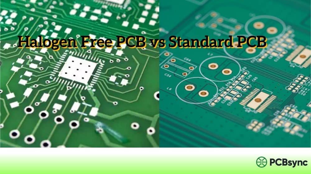
Halogen Free PCB vs Standard PCB: Making the Right Choice
The decision between halogen-free and standard PCB materials isn’t always straightforward. While the industry trend clearly favors halogen-free solutions, there are legitimate engineering and business considerations that should inform your material selection process for each specific project.
When to Choose Halogen Free PCB:
Your end customer has specified halogen-free requirements in their procurement specifications
The product will be sold in markets with strict environmental regulations (EU, California, Japan)
The application requires high thermal stability or will undergo multiple reflow cycles
Long-term reliability in humid or thermally challenging environments is critical
Your company has corporate sustainability commitments to uphold
The product has a long expected lifecycle and you want to future-proof against regulatory changes
Considerations for Standard FR4:
Cost-sensitive, high-volume consumer products where margins are extremely tight
Products with short market lifecycles that won’t face regulatory changes during their lifespan
Legacy designs where requalification costs would outweigh material benefits
Applications where the standard material performance is genuinely adequate for requirements
That said, I’ve observed a clear shift in the industry over the past five years. Many PCB fabricators are now stocking halogen-free materials as their default option, and the cost premium has decreased significantly as production volumes have scaled up. For new designs, my general recommendation is to default to halogen-free unless there’s a specific compelling reason not to—the technical benefits and future-proofing advantages typically outweigh the modest additional cost.
Implementation Best Practices for Transitioning to Halogen Free
If you’re planning to transition existing products or standardize on halogen-free materials for new designs, here’s a practical roadmap based on lessons learned from successful implementation projects:
Conduct a Requirements Assessment: Before selecting specific materials, clearly define your regulatory compliance requirements, end customer specifications, and technical performance needs. Document the thermal, mechanical, and electrical requirements your PCB must meet.
Engage Your Supply Chain Early: Work with your laminate supplier and PCB fabricator from the beginning of the design process. They can recommend appropriate halogen-free materials that meet your specifications and are readily available without extended lead times.
Request Material Data Sheets and Test Reports: Obtain complete technical data sheets including Dk, Df, Tg, Td, CTE, and moisture absorption values. Also request halogen content test certificates showing compliance with IEC 61249-2-21 or your required standard.
Build and Test Prototypes: Before committing to production volumes, build prototype boards and run them through your complete qualification testing process. Pay particular attention to thermal cycling, humidity exposure, and any application-specific stress tests.
Update Your Design Documentation: Revise your PCB fabrication drawings, stackup specifications, and assembly instructions to explicitly call out halogen-free material requirements. Include the specific laminate part numbers and acceptable equivalents.
Establish Incoming Inspection Procedures: Implement verification procedures to ensure incoming materials meet halogen-free specifications. This might include requesting lot-specific certificates of conformance or periodic third-party testing of samples.
Conclusion: The Future is Halogen-Free
Halogen free PCB technology has matured dramatically over the past decade. What began primarily as a regulatory compliance-driven requirement has evolved into a genuine performance advantage for many demanding applications. The compelling combination of improved thermal properties, better electrical insulation characteristics, lower moisture absorption, and demonstrated environmental responsibility makes halogen-free materials an increasingly smart choice even in applications where they’re not strictly mandated by customer requirements.
As you evaluate halogen-free options for your next design project, work closely with your laminate supplier and PCB fabrication partner. Material selection is only one piece of the puzzle—proper design-for-manufacturing practices and optimized production processes are equally important to realize the full benefits these advanced materials can deliver.
The electronics industry is clearly and irreversibly moving toward halogen-free as the new standard baseline. Positioning your products and supply chain ahead of this curve now will set you up well for future regulatory requirements, evolving customer expectations, and the competitive advantages that come with demonstrated environmental leadership in an increasingly sustainability-conscious marketplace.
The bottom line is this: halogen-free PCB technology has reached a level of maturity where the engineering risks are minimal, the performance benefits are real, and the environmental advantages are substantial. Whether you’re driven by customer requirements, regulatory compliance, technical performance, or corporate sustainability goals, investing in halogen-free materials represents a sound engineering decision for virtually any modern electronics application. The question is no longer whether to adopt halogen-free materials, but rather how quickly and comprehensively to implement them across your product portfolio.
Inquire: Call 0086-755-23203480, or reach out via the form below/your sales contact to discuss our design, manufacturing, and assembly capabilities.
Quote: Email your PCB files to Sales@pcbsync.com (Preferred for large files) or submit online. We will contact you promptly. Please ensure your email is correct.
Notes: For PCB fabrication, we require PCB design file in Gerber RS-274X format (most preferred), *.PCB/DDB (Protel, inform your program version) format or *.BRD (Eagle) format. For PCB assembly, we require PCB design file in above mentioned format, drilling file and BOM. Click to download BOM template To avoid file missing, please include all files into one folder and compress it into .zip or .rar format.


