Inquire: Call 0086-755-23203480, or reach out via the form below/your sales contact to discuss our design, manufacturing, and assembly capabilities.
Quote: Email your PCB files to Sales@pcbsync.com (Preferred for large files) or submit online. We will contact you promptly. Please ensure your email is correct.
Notes: For PCB fabrication, we require PCB design file in Gerber RS-274X format (most preferred), *.PCB/DDB (Protel, inform your program version) format or *.BRD (Eagle) format. For PCB assembly, we require PCB design file in above mentioned format, drilling file and BOM. Click to download BOM template To avoid file missing, please include all files into one folder and compress it into .zip or .rar format.
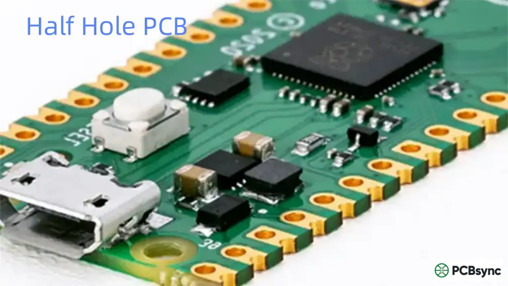
A comprehensive guide for PCB engineers covering half hole PCB design specifications, manufacturing processes, and practical soldering techniques for modular electronics.
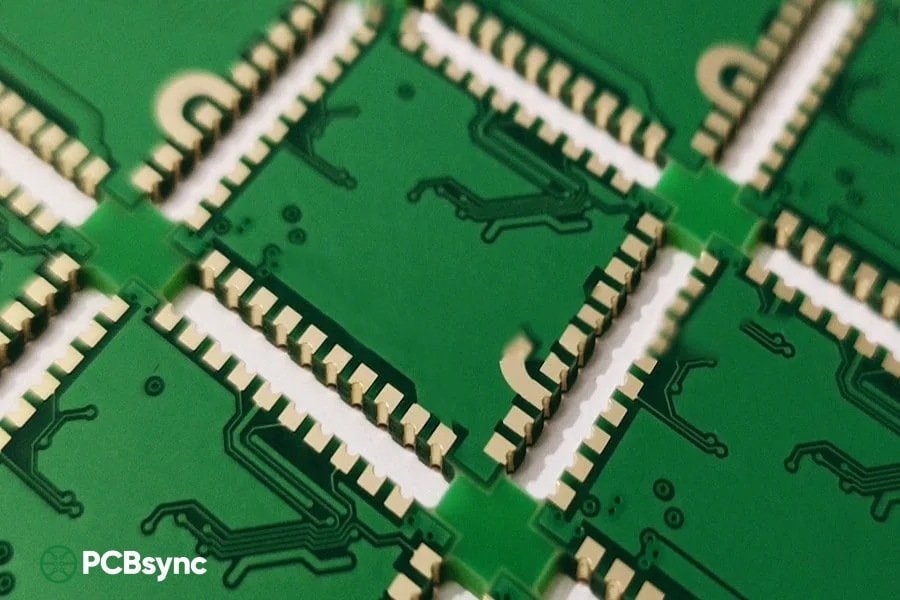
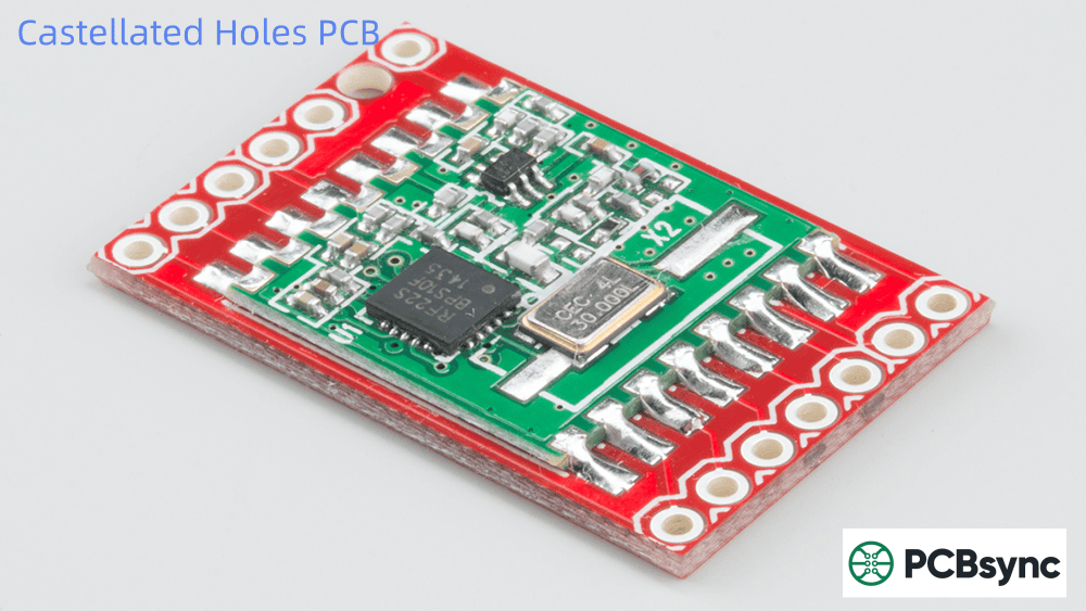
If you’ve ever worked with WiFi modules, Bluetooth boards, or any compact IoT device, you’ve probably encountered half hole PCB technology—even if you didn’t realize it at the time. Those neat semi-circular plated indentations along the edge of a module board? That’s what we’re talking about.
Half hole PCB (also known as castellated holes or plated half-holes) has become an essential technique in modern electronics manufacturing. As someone who’s spent years designing and troubleshooting board-to-board connections, I can tell you that understanding this technology properly can save you countless hours of debugging and rework.
The growth of IoT devices, wearables, and miniaturized electronics has made half hole PCB technology more relevant than ever. According to industry trends, the demand for compact modular PCB designs has increased significantly over the past few years. Manufacturers like ESP32, Raspberry Pi, and countless wireless module makers have standardized on castellated connections for their products.
In this guide, I’ll walk you through everything you need to know—from basic concepts to advanced design rules—so you can implement half hole PCB technology confidently in your next project. Whether you’re designing your first castellated module or looking to optimize an existing design, this comprehensive guide covers the practical knowledge you need.
A half hole PCB features semi-circular plated holes positioned along the board’s edge. These aren’t your regular through-holes cut in half randomly—they’re precision-engineered connection points designed specifically for board-to-board soldering.
The manufacturing process starts with drilling standard plated through-holes (PTH) at precise locations along the planned board edge. After copper plating, the board is routed through the center of these holes, creating the characteristic half-moon shape that gives castellated holes their name (from the resemblance to castle battlements).
The key difference between half hole PCB and standard edge connections is the plated interior surface. This copper-plated concave area provides an excellent landing pad for solder, creating mechanically strong and electrically reliable connections between a daughter board and mother board.
From a historical perspective, castellated holes emerged as engineers sought better ways to connect modular circuit boards without bulky connectors. Early versions appeared in military and aerospace applications where space and weight were critical concerns. Today, the technology has become mainstream, with millions of castellated modules manufactured annually for consumer and industrial electronics.
The typical castellated hole diameter ranges from 0.5 mm to 1.0 mm, with center-to-center spacing commonly at 0.8 mm to 1.27 mm (matching standard header pitches). This standardization makes it easy to design compatible footprints on your main board.
Alternative Names You’ll Encounter
The terminology can get confusing because different manufacturers and regions use different names for the same thing:
Castellated holes – The most common technical term
Plated half-holes – Descriptive term emphasizing the plating
Castellations – Shortened form often used in industry
Edge-plated holes – Sometimes used interchangeably
Stamp holes – Reference to their resemblance to postage stamp perforations
Regardless of what you call them, they all refer to the same board-to-board connection technology.
How Half Hole PCB Works
Understanding the working principle is crucial before diving into design. Here’s what happens during the connection process:
The daughter board (module) with half hole edges sits directly on the mother board’s SMD pads. During reflow soldering or hand soldering, solder wicks up into the concave plated surface of each half hole. This creates a fillet-shaped joint that provides both electrical connection and mechanical anchoring.
The physics behind this process involves capillary action. Molten solder naturally flows into the concave half-hole structure because the plated copper surface has excellent solder wettability. The surface tension of the molten solder draws it upward along the curved interior, creating a strong metallurgical bond between the module and the main PCB.
Two critical requirements must be met for proper half hole PCB connections:
Zero gap between boards – The module must sit flush against the main PCB surface. Any air gap compromises both electrical conductivity and mechanical strength.
Proper electrical contact – Physical contact alone isn’t sufficient. The solder joint must establish solid metallurgical bonding between the half hole plating and the pad below.
When done correctly, the resulting connection is often stronger than traditional pin header connections and significantly more compact.
Half Hole PCB Design Rules and Specifications
Getting the design parameters right is where most engineers either succeed or struggle. After reviewing specifications from major PCB manufacturers and working through numerous designs, here are the critical dimensions you need to follow.
Critical Design Specifications
Parameter
Minimum Value
Recommended Value
Half hole diameter
0.4 mm
0.6 mm – 0.8 mm
Hole-to-hole spacing (edge to edge)
0.5 mm
0.55 mm or greater
Annular ring width
0.18 mm (absolute)
0.25 mm – 0.30 mm
Pad-to-pad spacing
0.25 mm
0.3 mm or greater
Copper plating thickness
25 μm
25 μm – 50 μm
Board thickness range
0.8 mm
1.0 mm – 1.6 mm
Minimum board dimension
10 mm × 10 mm
Varies by manufacturer
Right-angle half hole diameter
1.2 mm
1.5 mm or larger
Pad Design Considerations
The pad size significantly affects solder joint reliability. For a typical 0.6 mm half hole, use a minimum pad diameter of 1.3 mm (hole diameter plus 0.7 mm). This ensures adequate annular ring on both top and bottom layers.
For inner layers on multilayer boards, maintain the same pad size and ensure the inner layer pads connect properly to the plated hole. This improves structural stability and prevents copper lifting during the routing process.
When designing the corresponding pads on your mother board, use SMD pads slightly larger than the half hole diameter. A 0.6 mm half hole works well with a 0.8 mm to 1.0 mm rectangular pad on the mother board. The extra pad area improves solder wetting and provides tolerance for placement variations.
Pro tip: Consider using teardrop-shaped pads for applications subject to vibration or thermal cycling. The gradual transition from trace to pad reduces stress concentration points.
Hole Positioning Requirements
Place the exact center of each half hole precisely on the board edge outline. This is critical—if the hole center is offset from the board edge, you’ll end up with either more or less than half the hole remaining after routing.
Key positioning rules:
At least 50% of the hole must remain inside the board after routing
Castellated pad edge to board edge distance should be at least 1 mm
Maintain at least 0.3 mm clearance between the hole cut line and internal copper layers
Oval castellated holes parallel to the board edge cannot be manufactured—avoid this design
Half Hole PCB Manufacturing Process
Understanding how half hole PCBs are manufactured helps you design for manufacturability and anticipate potential issues.
Step-by-Step Manufacturing Process
Step
Process
Details
1
Drilling
Standard PTH drilling at board edge locations using CNC drill equipment
2
Panel Plating
Electroless copper deposition followed by electrolytic copper plating to build wall thickness
3
Image Transfer
Photoresist application and circuit pattern imaging
4
Pattern Plating
Additional copper and tin plating on circuit pattern areas
5
Etching
Removal of unwanted copper to reveal circuit traces
6
Solder Mask
Application of protective solder mask layer with openings for half holes
7
Surface Finish
ENIG, HASL, or other surface treatment for solderability
8
Routing/Milling
CNC routing through hole centers to create half-hole profile (critical step)
9
Deburring
Removal of copper burrs through alkaline etching or mechanical methods
10
Inspection
Visual and electrical testing for defects, plating integrity, and dimensional accuracy
The Critical Routing Step
The routing (or milling) step is where half hole PCB manufacturing gets tricky. The CNC router must cut precisely through the center of each plated hole while maintaining the integrity of the remaining copper plating.
Here’s what happens mechanically: As the router bit (typically spinning clockwise at 20,000-30,000 RPM) cuts through the hole, it pushes against the copper on one side while pulling away from it on the other. On the “push” side, the copper remains firmly bonded to the substrate. On the “pull” side, there’s risk of copper burrs, peeling, or debris.
Quality manufacturers address this through:
Two-step drilling/milling processes
Specialized carbide routing bits (0.8-2.0 mm diameter)
Optimized feed rates (0.5-1.5 meters/minute)
Double V-shaped cutting tool paths
Post-routing deburring through alkaline etching
Important: Never use V-cut scoring on edges with castellated holes. The V-cut tool will pull on the copper and cause it to detach from the hole wall. Always specify CNC milling for castellated edges.
Uneven surface can clog small half holes, thermal stress on thin boards
Immersion Silver
Good for high-frequency applications, flat surface
Shorter shelf life, sensitive to handling
OSP
Low cost, environmentally friendly, flat surface
Limited shelf life, not suitable for multiple reflow cycles
Recommendation: For half hole PCBs, ENIG (Electroless Nickel Immersion Gold) is generally the best choice. It provides consistent results across all hole sizes and handles the routing process well. If your castellated holes are larger than 1 mm diameter, lead-free HASL can work, but ENIG remains more reliable overall.
Benefits of Half Hole PCB Technology
Why choose half hole PCB over traditional connection methods? Here are the practical advantages I’ve observed across dozens of projects:
Dramatic Space Savings
Traditional board-to-board connectors typically add 5-10 mm of height to your stack. Half hole connections? Essentially zero additional height. The module sits flush against the main board surface. For wearables, IoT sensors, and other space-constrained applications, this difference is often the deciding factor.
Cost Reduction
Eliminating connectors removes component costs, assembly steps, and potential failure points. While half hole PCB fabrication costs slightly more than standard boards, the overall system cost typically decreases. You’re also reducing your BOM complexity and inventory requirements.
Consider the typical connector cost: a simple 2×5 header pair might cost $0.10-0.30, but when you factor in the PCB real estate it consumes, the additional assembly step, and potential warranty returns from loose connections, the true cost is much higher. Half hole PCB eliminates all of these hidden costs while providing a superior connection.
Assembly Efficiency
Half hole modules can be placed and soldered in the same reflow pass as other SMD components. No separate connector insertion step, no additional soldering process. This streamlines production and reduces handling.
Improved Reliability
Soldered connections outperform mechanical connectors in several ways:
No insertion/removal wear
Better vibration resistance
Lower contact resistance
No oxidation at contact points over time
Tighter dust and moisture sealing between boards
Signal Integrity
Direct soldered connections through half holes provide shorter signal paths than connector-based solutions. For high-frequency applications like WiFi and Bluetooth modules, this translates to better signal quality and reduced EMI concerns.
The metallization of the PCB edges also helps prevent electromagnetic interference on inner layers and reduces the risk of electrostatic damage. This makes half hole PCB particularly suitable for sensitive RF circuits and high-speed digital signals.
Modular Design Flexibility
Half hole PCB enables true modular design approaches. You can design, test, and validate individual modules independently before final integration. This is particularly valuable for:
Separating certified RF sections from uncertified logic
Creating reusable building blocks across product lines
Isolating sensitive analog circuits from noisy digital sections
Enabling field-replaceable sub-assemblies
Allowing different teams to work on separate modules simultaneously
Thermal Management Benefits
Complex systems such as aerospace, telecommunications, and high-power devices often generate significant heat. Castellated circuit boards offer better heat dissipation compared to connector-based solutions because the soldered metal joint provides direct thermal coupling between boards. Heat can transfer through the copper plating into the mother board’s ground plane or thermal management features.
Common Applications
Half hole PCB technology has found its way into virtually every sector of electronics manufacturing. Here are the most common use cases:
PLC modules, motor controllers, sensor interface boards, HMI modules
Telecommunications
Base station modules, router components, 5G antenna modules
Board-to-Board Soldering Guide
Whether you’re doing production assembly or prototyping, proper soldering technique is essential for reliable half hole PCB connections.
Reflow Soldering (Production)
For production volumes, reflow soldering is the standard approach:
Apply solder paste to the SMD pads on the mother board using stencil printing
Place the castellated module using pick-and-place equipment (treat it like any other SMD component)
Run through standard reflow profile
During reflow, solder paste wicks up into the half holes, creating the characteristic fillet joint
The concave shape of the half holes naturally draws solder upward through capillary action. After cooling, you’ll see a shiny solder fillet visible along each castellated edge.
Hand Soldering (Prototyping)
For prototypes and rework, hand soldering works well with the right technique:
Prepare the pads: Apply flux to both the mother board pads and module half holes
Tack one corner: Pre-tin one pad, place the module, and heat to tack it in position
Verify alignment: Check that all half holes align with their corresponding pads before proceeding
Solder remaining pins: Heat each pad/half-hole junction while feeding solder into the joint
Clean flux residue: Use isopropyl alcohol and a brush to remove flux
Inspect joints: Look for complete solder coverage on each half hole
Tip: Use a chisel tip sized appropriately for your pad pitch. The iron should contact both the pad and the castellated via simultaneously for best heat transfer.
Common Issues and How to Avoid Them
Even experienced engineers run into problems with half hole PCB. Understanding these common pitfalls before you start designing can save significant time and money. Here are the most common issues and their solutions:
Issue
Cause
Solution
Copper burrs
Poor routing process or wrong tool direction
Use quality manufacturer with proper deburring; specify ENIG finish
Copper peeling
V-cut used instead of CNC milling; insufficient plating thickness
Verify reflow profile; clean surfaces before soldering; add stress relief
Design Software Implementation
Setting up half holes in your EDA tool isn’t always intuitive. Here’s how to approach it in common software:
General Approach (Works in Most Tools)
Create standard plated through-hole pads at your desired castellated locations
Position the pad center exactly on the board outline
Ensure the pad appears on all copper layers (including inner layers for multilayer boards)
Include the half holes in your drill file (PTH layer, not NPTH)
When ordering, select “Castellated Holes” option if available
KiCad Specific Tip
In KiCad, the simplest approach is to use standard through-hole pads and run your board outline through the middle of those pads. KiCad will handle the rest automatically when you generate Gerber files.
Altium Designer Tip
Use the Tools menu → Create Region from Selected Primitives function to define your castellated pad structure. Altium has built-in support for castellated holes in recent versions.
Pre-Production Quality Checklist
Before sending your half hole PCB design for fabrication, run through this comprehensive verification checklist. Catching issues at the design stage is far cheaper than discovering them during production or, worse, in the field.
Half hole diameter ≥ 0.5 mm (preferably 0.6 mm or larger)
Hole-to-hole edge spacing ≥ 0.55 mm
Annular ring ≥ 0.25 mm on all layers
Hole centers exactly on board outline
No oval holes parallel to board edge
Half holes defined as plated through holes in drill file
ENIG or appropriate surface finish specified
Board dimension ≥ 10 mm × 10 mm
No V-cut scoring specified on castellated edges
Matching SMD pad array designed for mother board
“Castellated holes” option selected when ordering
After receiving your boards, perform incoming inspection. Check for copper burrs in the half holes using a magnifying glass or microscope. Look for any signs of copper peeling or delamination along the routed edges. Verify dimensional accuracy by measuring a sample of hole diameters and positions against your design specifications.
Useful Resources
Here are some valuable resources for further learning and reference:
Industry Standards
IPC-7351: Generic Requirements for Surface Mount Design and Land Pattern Standard
IPC-A-600: Acceptability of Printed Boards (includes castellated hole criteria)
IPC-6012: Qualification and Performance Specification for Rigid Printed Boards
Altium Academy Video Series on Castellated PCB Design
Frequently Asked Questions
What is the minimum hole size for half hole PCB?
The absolute minimum is typically 0.4 mm, but most manufacturers recommend 0.5 mm or larger for reliable results. For best quality and easier manufacturing, use 0.6 mm to 0.8 mm diameter holes. Smaller holes require advanced fabrication capabilities and typically cost more.
How much does half hole PCB cost compared to standard PCB?
Half hole PCB typically costs 15-30% more than equivalent standard PCB due to the additional manufacturing steps—specifically the precision routing and deburring processes. However, when you factor in eliminated connector costs and simplified assembly, total system cost often decreases. The cost premium also decreases at higher volumes.
Can I use half hole PCB for high-frequency applications?
Yes, half hole PCB connections work well for high-frequency applications including WiFi (2.4 GHz and 5 GHz), Bluetooth, and even some RF applications. The direct soldered connection provides lower impedance and shorter signal paths compared to connector-based solutions. For best results, use ENIG surface finish and maintain proper ground plane continuity between boards.
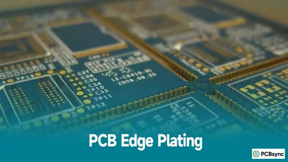
What’s the difference between castellated holes and edge plating?
While related, they’re different processes. Castellated holes are individual half-holes with separate plated surfaces, each connecting specific signals. Edge plating covers the entire board edge with copper, typically used for EMI shielding or grounding purposes. Castellated holes are a more specialized form of edge metallization designed specifically for board-to-board connections.
How do I rework a module with castellated holes?
Reworking castellated connections requires careful heat application. Use a hot air station with appropriate nozzle size, heating all joints simultaneously. Apply flux before heating. Once the solder melts, gently lift the module with tweezers. Clean both the module and PCB pads with solder wick, apply fresh flux and solder, then reattach. For valuable modules, consider using a preheater to reduce thermal shock.
Final Thoughts
Half hole PCB technology has become indispensable for modern electronics design. Whether you’re building IoT devices, wireless modules, or any space-constrained application, mastering castellated hole design gives you a powerful tool for creating compact, reliable, and cost-effective products.
As electronic devices continue to shrink in size while increasing in complexity, castellated hole technology will play an increasingly important role in PCB design and manufacturing. The combination of space savings, cost reduction, improved reliability, and assembly efficiency makes it an attractive option for a wide range of applications.
The key takeaways:
Follow the minimum specifications (0.5 mm diameter, 0.55 mm spacing, 0.25 mm annular ring)
Choose ENIG surface finish for best results
Always specify CNC routing (never V-cut) for castellated edges
Work with a manufacturer experienced in half hole fabrication
Design matching SMD pads on your mother board for proper alignment
With proper design and manufacturing, half hole PCB connections can be just as reliable as any other interconnect technology—often more so. Take the time to get your design right, and you’ll have a robust solution that serves your product well for years to come.
Have questions about your specific half hole PCB design? Feel free to consult with your PCB manufacturer’s engineering team—most reputable fab houses offer free DFM review that can catch potential issues before production.
Inquire: Call 0086-755-23203480, or reach out via the form below/your sales contact to discuss our design, manufacturing, and assembly capabilities.
Quote: Email your PCB files to Sales@pcbsync.com (Preferred for large files) or submit online. We will contact you promptly. Please ensure your email is correct.
Notes: For PCB fabrication, we require PCB design file in Gerber RS-274X format (most preferred), *.PCB/DDB (Protel, inform your program version) format or *.BRD (Eagle) format. For PCB assembly, we require PCB design file in above mentioned format, drilling file and BOM. Click to download BOM template To avoid file missing, please include all files into one folder and compress it into .zip or .rar format.


