Inquire: Call 0086-755-23203480, or reach out via the form below/your sales contact to discuss our design, manufacturing, and assembly capabilities.
Quote: Email your PCB files to Sales@pcbsync.com (Preferred for large files) or submit online. We will contact you promptly. Please ensure your email is correct.
Notes: For PCB fabrication, we require PCB design file in Gerber RS-274X format (most preferred), *.PCB/DDB (Protel, inform your program version) format or *.BRD (Eagle) format. For PCB assembly, we require PCB design file in above mentioned format, drilling file and BOM. Click to download BOM template To avoid file missing, please include all files into one folder and compress it into .zip or .rar format.
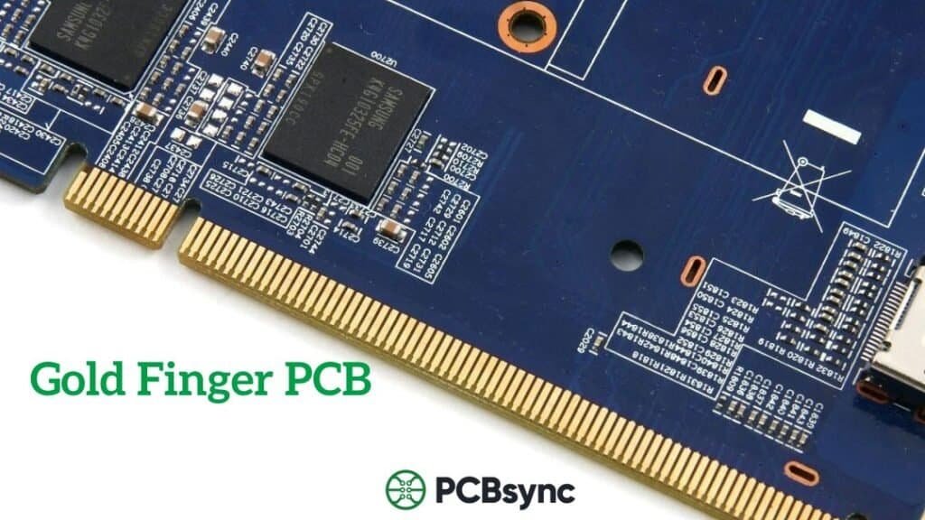
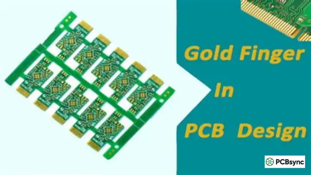
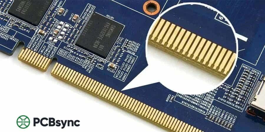
If you’ve ever pulled apart a computer or examined a graphics card, you’ve probably noticed those shiny gold-plated contacts along the edge of the circuit board. Those are gold fingers—and they’re far more critical to electronic functionality than most people realize.
I’ve been designing PCBs for over a decade, and I still find it fascinating how these small connectors enable billions of devices worldwide to communicate reliably. Whether you’re engineering memory modules, developing industrial control systems, or working on consumer electronics, understanding gold finger PCB design is essential for creating robust, long-lasting products.
This guide covers everything you need to know about gold finger PCBs—from the fundamentals of what they are and why gold is the preferred material, to detailed specifications, design rules, plating processes, and real-world applications. Let’s get into it.
A gold finger PCB refers to a printed circuit board that features gold-plated connectors along its edge. These connectors—called “gold fingers” because of their finger-like shape and gold coloring—serve as the interface between the PCB and external devices or motherboards.
When you insert a RAM stick into your computer’s memory slot or plug a graphics card into a PCIe slot, the gold fingers on those components make direct contact with the slot’s spring contacts. This creates the electrical pathway that allows data and power to flow between the component and the main system.
The term “edge connector” is sometimes used interchangeably with gold fingers, though technically they’re slightly different. Gold fingers specifically refer to the gold-plated pads on the PCB edge, while edge connectors refer to the receiving sockets that accept these fingers.
From a manufacturing perspective, gold fingers represent one of the more demanding aspects of PCB fabrication. The plating process requires precise control, the beveling must be exact, and the final product must meet stringent quality standards. A poorly manufactured gold finger can result in intermittent connections, signal integrity issues, or complete failure to communicate with the host system.
It’s worth noting that approximately 7% of the world’s gold can be found in discarded electronic devices, with a significant portion of that gold residing in PCB gold fingers. A ton of electronic waste can contain up to 300 grams of gold—60 times more than what you’d extract from a ton of gold ore. This gives you some perspective on just how widely gold fingers are used across the electronics industry.
Why Use Gold for PCB Connectors?
Gold isn’t chosen for its appearance—it’s selected because of its exceptional electrical and mechanical properties:
Superior Conductivity: Gold provides excellent electrical conductivity with minimal signal loss, making it ideal for high-speed data transmission in applications like DDR5 memory and PCIe 5.0.
Corrosion Resistance: Unlike copper or nickel, gold doesn’t oxidize when exposed to air or moisture. This means gold finger connections remain reliable for years, even in harsh environments.
Wear Resistance: Hard gold plating (when alloyed with cobalt) can withstand thousands of insertion and removal cycles without degrading.
Low Contact Resistance: Gold maintains consistent low-resistance connections even under light pressure, which is critical for edge connector applications.
High Ductility: Gold’s excellent ductility allows it to conform to mating surfaces under pressure, increasing the effective contact area and improving signal transmission efficiency.
Chemical Stability: Gold is chemically inert, meaning it won’t react with most environmental contaminants that could degrade connection quality over time.
While copper and silver technically have higher electrical conductivity than gold, they both suffer from oxidation issues that make them unsuitable for exposed contact surfaces. Silver tarnishes quickly when exposed to sulfur compounds in the atmosphere, while copper forms a non-conductive oxide layer. Gold’s combination of good conductivity and exceptional stability makes it the only practical choice for high-reliability connector applications.
Types of Gold Finger PCBs
Gold fingers come in several configurations, each suited for different applications. Understanding these types helps you choose the right design for your project.
Type
Description
Common Applications
Regular (Flush)
Equal-length pads arranged symmetrically with uniform spacing
Graphics cards, network cards, PCI/PCIe slots
Long-Short (Uneven)
Pads of varying lengths; longer fingers make contact first during insertion
USB drives, SD card readers, hot-swap devices
Segmented
Fingers with intentional gaps or interruptions in the contact surface
The long-short configuration is particularly clever from an engineering perspective. By having power and ground pins make contact before signal pins, it prevents voltage spikes that could damage sensitive components during hot-swapping.
Choosing the right gold finger type isn’t just about aesthetics—it directly impacts functionality. For instance, if you’re designing a USB flash drive that users will plug and unplug hundreds of times, the long-short configuration provides hot-swap protection and guides the insertion. For a graphics card that sits in a slot for years without removal, regular flush fingers are more appropriate and cost-effective.
Segmented gold fingers are less common but serve specialized purposes. The intentional gaps in the contact surface can prevent short circuits during partial insertion, create isolated power domains, or accommodate specific connector designs. You’ll often see these in industrial equipment where fail-safe operation is critical.
Gold Finger Plating: ENIG vs. Hard Gold
Not all gold plating is created equal. The two main types used for PCB gold fingers have very different characteristics and suitable applications.
Electroplated Hard Gold
Hard gold electroplating is the industry standard for gold fingers that will experience repeated insertion and removal cycles. The process involves electroplating a gold-cobalt alloy (typically 5-10% cobalt) over a nickel underlayer.
Key characteristics:
Thickness range: 30-50 microinches (0.76-1.27 µm) for high-durability applications
Hardness: 150-200 HV (Vickers hardness) due to cobalt content
ENIG is a more cost-effective option but comes with limitations for gold finger applications. The immersion gold layer is much thinner (typically 2-5 microinches) and softer than electroplated hard gold.
When to use ENIG for gold fingers:
Low insertion-cycle applications (less than 25 insertions)
Cost-sensitive prototypes
Applications where the connection is semi-permanent
Plating Comparison Table
Property
Hard Gold (Electroplated)
ENIG (Immersion Gold)
Gold Thickness
30-50 µin (0.76-1.27 µm)
2-5 µin (0.05-0.13 µm)
Nickel Underlayer
100-200 µin (2.5-5 µm)
118-236 µin (3-6 µm)
Hardness
150-200 HV (Hard)
50-90 HV (Soft)
Insertion Cycles
500-1,000+
<25
Relative Cost
Higher
Lower
Best For
RAM, graphics cards, industrial cards
Prototypes, low-wear applications
IPC Standards for Gold Finger PCBs
The IPC (Association Connecting Electronics Industries) has established comprehensive standards for gold finger manufacturing. If you’re working on commercial or industrial products, familiarity with these standards is non-negotiable.
Key IPC Standards
IPC-4556: Specification for ENEPIG plating (Electroless Nickel/Electroless Palladium/Immersion Gold)
IPC-6012: Qualification and Performance Specification for Rigid PCBs (includes gold finger requirements)
IPC-A-600: Acceptability of Printed Boards (visual inspection criteria)
IPC-6010: Qualification and Performance Specification for Rigid PCBs (Class requirements)
IPC Class Requirements for Gold Thickness
IPC Class
Minimum Gold Thickness
Application Examples
Class 1
5-10 µin (0.13-0.25 µm)
Consumer electronics, general-purpose devices
Class 2
30 µin (0.76 µm) minimum
Industrial equipment, communications, computers
Class 3
50 µin (1.27 µm) minimum
Aerospace, military, medical, high-reliability
The IPC also specifies that gold plating should contain 5-10% cobalt for maximum rigidity and wear resistance. This is a detail that many newer engineers overlook, but it makes a significant difference in long-term reliability.
The history of these standards is worth understanding. The IPC first established gold finger production standards in 2002, updated them with IPC-4556 in 2012, and released the current IPC-A-600 and IPC-6010 standards in 2015. These standards continue to evolve as new technologies like DDR5 memory and PCIe 6.0 push the boundaries of what gold fingers need to handle.
For Class 3 applications (aerospace, military, medical), the standards are particularly stringent. Not only is thicker gold required, but additional testing including salt spray exposure, thermal cycling, and accelerated aging may be mandated. If you’re working on a high-reliability project, get a copy of the relevant IPC specifications and make sure your PCB manufacturer understands the requirements.
Getting the design right is crucial. I’ve seen plenty of boards come back from manufacturing with unusable gold fingers because basic design rules weren’t followed. Here’s what you need to know.
Critical Spacing Requirements
Board Edge Clearance: Maintain at least 0.5mm (20 mil) between gold fingers and the PCB board outline. This prevents damage during the beveling process.
PTH Clearance: Keep plated through-holes (PTHs) at least 1.0mm away from gold fingers. Closer placement can cause shorts or manufacturing defects.
SMD Component Clearance: No SMD components, solder pads, or vias should be placed within 1.0mm of the gold finger area.
Solder Mask Clearance: The solder mask opening should extend approximately 4 mil (0.1mm) beyond the copper trace on each side.
Maximum Finger Length: Gold fingers should not exceed 40mm in length. Longer fingers are more prone to damage during handling.
Solder Mask and Silkscreen Considerations
One area that trips up even experienced designers is solder mask handling around gold fingers. The gold finger area must have a continuous solder mask opening—no solder mask should extend into the contact zone. Here’s why this matters:
Solder mask material can build up between fingers during repeated insertion, eventually causing poor contact
The solder mask window should extend approximately 10 mil (0.25mm) beyond the board edge
No solder mask openings should be placed within 2mm of the gold finger area
Silkscreen printing must be kept well away from gold fingers—any ink in the contact zone will cause reliability issues
I’ve seen boards where solder mask ink contaminated the gold fingers during PCB manufacturing, resulting in high contact resistance that only appeared after several insertion cycles. By the time the problem was discovered, thousands of boards were affected. Double-check your solder mask and silkscreen keepouts before sending files to manufacturing.
Inner Layer Copper Removal
This is something that catches a lot of designers off guard: all inner layers beneath the gold fingers must have copper removed. Here’s why this matters:
During edge beveling, exposed inner layer copper looks unprofessional and can cause reliability issues
Copper removal width should be at least 3mm from the board edge
For PCIe designs, all copper within the gold finger area must be removed per the specification
Beveling (Chamfering) Requirements
Beveling creates an angled edge on the PCB to allow smooth insertion into mating connectors. Without proper beveling, you risk damaging both the gold fingers and the connector slot.
Bevel Angle
Typical Use
Board Thickness
Notes
20°
Special applications
Thinner boards
Shallow angle, requires care
30°
Standard default
1.6mm typical
Most common choice
45°
Common alternative
1.6mm – 2.4mm
Easier insertion, wider clearance
60°
Special applications
Thicker boards
Steepest common angle
Important: The residual board thickness after beveling should be at least 0.25mm-0.5mm. Calculate your bevel depth carefully based on board thickness and angle to avoid cutting into the gold fingers.
The beveling process is typically performed using automated milling equipment. For boards smaller than 40x40mm, the chamfer is usually milled first, followed by the outline milling in a second operation. This requires positioning holes on both sides of the electroplated edge for precise alignment. Larger boards can be beveled as part of the normal depanelization process.
When panelizing boards with gold fingers, consider the finger orientation. The standard approach is to position gold fingers facing outward from the panel center—this simplifies the beveling operation and prevents damage during depanelization. If you’re using V-scoring for panel separation, note that boards with gold fingers on the V-score edge cannot be chamfered properly since the fingers would end up in the middle of the separated board.
Gold Finger Plating Process: Step by Step
Understanding how gold fingers are manufactured helps you design better boards and troubleshoot issues when they arise. Here’s the typical hard gold electroplating process:
Surface Preparation: The PCB is masked, leaving only the gold finger area exposed. The copper surface is cleaned with acid to remove oxidation, followed by a thorough water rinse.
Mechanical Cleaning: Abrasive cleaning removes any remaining contaminants and creates a surface profile for better adhesion.
Nickel Plating: A nickel layer (3-6 µm / 100-200 µin) is electroplated onto the copper. This acts as a barrier layer preventing copper diffusion into the gold and improves adhesion.
Gold Electroplating: Hard gold (1-2 µm / 30-50 µin) containing 5-10% cobalt is electroplated over the nickel. The cobalt content provides the hardness needed for wear resistance.
Beveling: The connector edges are beveled at the specified angle (typically 30° or 45°) to facilitate smooth insertion.
Inspection and Testing: Visual inspection with magnification, tape adhesion testing, and thickness verification using XRF measurement.
A few critical notes about the plating chemistry: The gold plating solution typically uses potassium gold cyanide (Au(CN)₂) as the gold source. This is a toxic compound that requires careful handling and proper wastewater treatment—one reason why not all PCB manufacturers offer gold finger plating. The cobalt is added as a complexing agent that co-deposits with the gold, creating the hard gold-cobalt alloy.
The sequence of operations is also important. Gold finger plating happens after solder mask application but before final surface finish (like HASL or OSP) is applied to the rest of the board. This timing ensures the gold fingers get the correct hard gold plating while allowing other surface finishes for solderable areas.
Temperature control during plating is critical for achieving the right gold grain structure and hardness. The plating bath is typically maintained at 50-65°C, with precise current density control to ensure uniform deposition across all gold finger pads. Variations in temperature or current density can result in gold that’s too soft, too brittle, or non-uniform in thickness.
Quality Testing for Gold Finger PCBs
Before any gold finger PCB ships, it should pass several quality checks. Here’s what manufacturers typically verify:
Visual Inspection
Using magnification (typically 10x-20x), inspectors verify that the gold surface is smooth, uniform in color, and free from defects including scratches, pitting, exposed nickel, excess plating, and contamination.
Tape Adhesion Test
Per IPC recommendations, pressure-sensitive tape is applied firmly to the gold fingers and then removed. If gold plating transfers to the tape, it indicates poor adhesion—a failure that requires rejection of the board.
Thickness Measurement
X-Ray Fluorescence (XRF) is the industry standard for non-destructive thickness measurement. XRF can measure both the gold and nickel layer thicknesses with precision of ±1 microinch. Cross-sectional analysis may be used for validation during development but destroys the sample.
Beta backscatter is another non-destructive technique available for thickness measurement. It works by analyzing the reflection of beta particles from the gold surface and can provide accurate readings for both gold and nickel layers. While slightly less precise than XRF in some applications, it’s a viable alternative for quality control.
For high-reliability applications, you may also want to specify microsection analysis on sample boards from each production lot. This involves cutting through the gold finger area, polishing the cross-section, and examining it under a microscope. While destructive, it provides definitive verification of layer structure, adhesion, and any potential defects like voids or delamination at the interfaces.
Common Applications of Gold Finger PCBs
Gold fingers are everywhere in modern electronics. Here are the major application areas:
Computing and Data Centers
Memory Modules (DIMMs): DDR4 and DDR5 RAM sticks use gold fingers for connection to motherboard memory slots
Graphics Cards: PCIe x16 slots require robust gold finger connections for high-bandwidth GPU communication
Network Interface Cards: Server NICs use gold fingers for reliable high-speed network connectivity
Storage Controllers: RAID cards and NVMe adapters connect via PCIe gold finger interfaces
Consumer Electronics
Smartphones: SIM card slots and internal module connections use gold finger technology
USB Flash Drives: The exposed contacts on USB-A connectors are gold fingers
SD Cards and Memory Cards: The contact strips on removable storage cards
Gaming Consoles: Cartridge-based systems and expansion slots
Industrial and Automotive
PLC Modules: Industrial controllers use gold finger connections for I/O modules and expansion cards
Test Equipment: Oscilloscopes, spectrum analyzers, and other instruments with modular designs
Automotive ECUs: In-vehicle infotainment and ADAS modules often use gold finger connections
Communication Base Stations: 5G equipment and backplane systems rely on gold fingers for reliable RF connections
High-Frequency and High-Speed Applications
As data rates continue to increase (PCIe 6.0 operates at 64 GT/s, DDR5 at up to 6400 MT/s), gold finger design becomes increasingly critical for signal integrity. At these speeds, gold’s low skin effect and smooth surface finish reduce signal attenuation and reflections.
For high-frequency applications above 10 GHz, consider these additional factors:
Copper removal beneath gold fingers reduces impedance mismatch between the fingers and controlled-impedance traces
Surface roughness of the gold plating affects high-frequency losses—smoother is better
Nickel underlayer can introduce parasitic inductance at very high frequencies—some specifications require minimum nickel thickness while maintaining adhesion
The ESD protection benefits of copper removal beneath fingers become even more important as component geometries shrink
Common Problems and How to Avoid Them
After years of working with gold finger PCBs, I’ve seen the same problems come up repeatedly. Here’s how to prevent them:
Problem
Cause
Prevention
Poor adhesion / peeling
Inadequate surface prep, contamination
Proper cleaning, tape test during QC
Exposed inner copper
Inner layers not copper-cleared
Remove copper >3mm from edge on all layers
Shortened fingers after bevel
Fingers too close to board edge
Calculate safe distance based on thickness and angle
Poor contact reliability
Gold too thin, wrong plating type
Use hard gold ≥30µin for high-cycle apps
Difficult insertion
Missing or incorrect bevel angle
Always specify beveling in fabrication notes
Useful Resources and References
For those who want to dig deeper into gold finger PCB specifications and standards, here are the essential resources:
What is the standard gold thickness for PCB gold fingers?
For high-reliability applications requiring frequent insertion and removal (like RAM modules or graphics cards), the standard is 30-50 microinches (0.76-1.27 µm) of hard gold over 100-200 microinches of nickel. For prototypes or low-cycle applications, thinner plating down to 5-10 microinches may be acceptable. The IPC-6012 Class 2 specification requires a minimum of 30 microinches for dedicated service electronics.
Can I use ENIG instead of hard gold for my gold fingers?
ENIG (Electroless Nickel Immersion Gold) can be used for gold fingers, but with significant limitations. ENIG produces a much thinner gold layer (2-5 microinches) that’s also softer than electroplated hard gold. This makes it suitable only for applications with fewer than 25 insertion cycles and where the connection will be semi-permanent. For anything requiring regular plugging and unplugging—like memory slots, graphics cards, or test fixtures—hard gold electroplating is strongly recommended.
Why do gold fingers need to be beveled?
Beveling (also called chamfering) creates an angled edge on the PCB that allows the gold fingers to slide smoothly into mating connectors. Without beveling, the sharp 90-degree edge of the PCB can catch on the connector’s spring contacts, making insertion difficult and potentially damaging both the gold fingers and the connector slot. Standard bevel angles are 30° or 45°, depending on board thickness and connector requirements.
How many insertion cycles can gold fingers withstand?
With proper hard gold plating (30-50 microinches with 5-10% cobalt content), gold fingers can typically withstand 500 to 1,000+ insertion and removal cycles while maintaining reliable electrical contact. The actual durability depends on gold thickness, hardness (cobalt content), nickel underlayer quality, and the specific connector design. ENIG-plated fingers, being softer and thinner, are typically rated for fewer than 25 cycles.
What is the difference between gold fingers and edge connectors?
The terms are related but refer to different components. Gold fingers are the gold-plated contact pads on the edge of a PCB—they’re part of the circuit board itself. Edge connectors (or card edge connectors) are the receiving sockets that accept the gold fingers, typically mounted on a motherboard or backplane. Together, they form a complete connection system. Think of gold fingers as the “plug” and edge connectors as the “socket.”
Wrapping Up
Gold finger PCBs remain one of the most reliable and widely-used connection methods in electronics. Whether you’re designing memory modules, graphics cards, industrial controllers, or any device that needs robust, repeatable connections, understanding gold finger specifications, design rules, and manufacturing processes is essential for success.
The key takeaways from this guide:
Use hard gold electroplating (30-50 µin) for applications requiring repeated insertion cycles
Follow IPC spacing requirements—minimum 0.5mm from board edge, 1.0mm from PTHs
Always remove inner layer copper beneath the gold finger area
Specify appropriate beveling (typically 30° or 45°) in your fabrication notes
Verify plating quality with visual inspection, tape tests, and XRF thickness measurement
Get these fundamentals right, and your gold finger PCBs will provide years of reliable service. Have questions about a specific application or design challenge? Feel free to reach out or leave a comment below.
About this guide: This article was written from the perspective of a PCB design engineer with over a decade of experience in consumer electronics, industrial controls, and high-reliability applications. The specifications and best practices shared here reflect current industry standards as of 2025.
Inquire: Call 0086-755-23203480, or reach out via the form below/your sales contact to discuss our design, manufacturing, and assembly capabilities.
Quote: Email your PCB files to Sales@pcbsync.com (Preferred for large files) or submit online. We will contact you promptly. Please ensure your email is correct.
Notes: For PCB fabrication, we require PCB design file in Gerber RS-274X format (most preferred), *.PCB/DDB (Protel, inform your program version) format or *.BRD (Eagle) format. For PCB assembly, we require PCB design file in above mentioned format, drilling file and BOM. Click to download BOM template To avoid file missing, please include all files into one folder and compress it into .zip or .rar format.


