Inquire: Call 0086-755-23203480, or reach out via the form below/your sales contact to discuss our design, manufacturing, and assembly capabilities.
Quote: Email your PCB files to Sales@pcbsync.com (Preferred for large files) or submit online. We will contact you promptly. Please ensure your email is correct.
Notes: For PCB fabrication, we require PCB design file in Gerber RS-274X format (most preferred), *.PCB/DDB (Protel, inform your program version) format or *.BRD (Eagle) format. For PCB assembly, we require PCB design file in above mentioned format, drilling file and BOM. Click to download BOM template To avoid file missing, please include all files into one folder and compress it into .zip or .rar format.
Glass PCB Explained: Substrate Types & Industry Uses
The printed circuit board industry has come a long way from the early days of simple copper-clad boards. Today, manufacturers are pushing boundaries with advanced substrate materials, and glass PCB technology stands at the forefront of this evolution. If you’re designing electronics that demand precision, transparency, or exceptional thermal performance, understanding glass PCBs isn’t just helpful—it’s essential.
Glass substrates have quietly moved from laboratory curiosities to production-ready solutions. Major electronics manufacturers now specify glass PCBs for applications ranging from smartphone displays to 5G base stations. The technology addresses limitations that have long frustrated engineers working with conventional materials—particularly when it comes to thermal management and dimensional stability.
This guide breaks down everything you need to know about glass substrate circuit boards: what they are, how they differ from traditional FR-4, the various types available, and where they make the most sense for your projects. Whether you’re an engineer exploring new materials or a procurement specialist evaluating options, you’ll find practical insights here.
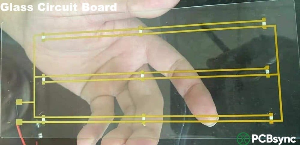
A glass PCB is a printed circuit board that uses glass as its primary substrate material instead of conventional options like FR-4 (fiberglass-reinforced epoxy resin). The glass substrate provides a stable, transparent foundation for mounting electronic components and routing electrical connections.
Unlike standard PCBs where the internal circuitry remains hidden beneath opaque green solder mask, glass PCBs can be designed to be partially or fully transparent. This opens up design possibilities that simply aren’t achievable with traditional materials.
The conductive traces on glass PCBs are typically made using transparent conductive materials like Indium Tin Oxide (ITO) or ultra-thin copper layers. When UV-curable masks are applied to transfer circuit patterns, manufacturers can achieve remarkably fine track widths—making glass substrates particularly attractive for high-density applications.
Calculate estimated manufacturing costs for your Glass PCB project based on specifications.
📊 Cost Estimation Results
Board Area
–
Unit Price (Est.)
–
Total Cost (Est.)
–
Price per cm²
–
💡Cost Tip: Glass PCB manufacturing costs 3-8x more than FR4 due to specialized equipment and handling. Order larger quantities for better unit pricing. Contact PCBSync for accurate quotes.
Glass Substrate Material Selection Guide
Choose the optimal glass substrate based on your application requirements.
🎯 Recommended Material
🔬
Borosilicate Glass
Best balance of thermal stability, transparency, and cost for LED applications.
CTE
3.3 ppm/°C
Max Temp
450°C
Dk Value
4.6
Cost Factor
1.5x
Glass Type
CTE (ppm/°C)
Max Temp
Dk
Best For
Soda-lime
9.0
250°C
7.0
Basic displays, cost-sensitive
Borosilicate
3.3
450°C
4.6
LED, sensors, general use
Quartz/Fused Silica
0.5
1000°C
3.8
High-temp, RF applications
Sapphire
5.8
1800°C
9.4
Extreme conditions, optical
Thermal Performance Calculator
Analyze thermal characteristics and heat dissipation for your Glass PCB design.
🌡️ Thermal Analysis Results
Thermal Resistance
–
Temperature Rise
–
Junction Temp (Est.)
–
Thermal Rating
–
Heat Dissipation Capacity
PoorModerateGoodExcellent
⚠️Design Note: Glass has lower thermal conductivity than metal-core PCBs. For high-power applications, consider thermal vias, heat spreaders, or sapphire substrate for better heat management.
Glass PCB Design Best Practices
Essential guidelines for successful Glass PCB design and manufacturing.
✅ Trace Design Guidelines
✓ Minimum trace width: 75µm (0.075mm) for standard, 50µm for fine pitch
✓ Minimum spacing: 75µm between traces
✓ Use curved traces instead of sharp 90° angles to reduce stress
✓ Add teardrops at pad-to-trace connections
✓ Copper thickness typically 9-35µm for glass substrates
⚠️ Critical Considerations
! Glass is brittle – design panels with proper support structures
! CTE mismatch between glass and components – use flexible adhesives
! Via processing is challenging – minimize via count when possible
! Edge handling requires smooth finish to prevent cracking
! Solder mask adhesion differs from FR4 – verify compatibility
🔧 Manufacturing Recommendations
✓ Specify edge chamfering or polishing to reduce breakage
✓ Use laser drilling for vias (mechanical drilling risks cracking)
✓ Consider TGV (Through Glass Via) technology for reliable interconnects
✓ Panel size typically limited to 300x400mm for handling
✓ ITO alternative: Use ITO (Indium Tin Oxide) for transparent conductors
Glass PCB vs Other Substrates
Compare Glass PCB with FR4, Ceramic, and Aluminum substrates for your application.
Property
Glass PCB
FR4
Ceramic
Aluminum
Transparency
Excellent
None
None
None
Thermal Conductivity
1.0-1.4 W/mK
0.3 W/mK
24-180 W/mK
1-2 W/mK
CTE (ppm/°C)
3.3-9.0
14-17
6-8
23
Dielectric Constant (Dk)
3.8-7.0
4.2-4.8
9-10
N/A
Max Temperature
250-1000°C
130°C
300-1000°C
150°C
RF Performance
Excellent
Good
Excellent
Poor
Cost Factor
3-8x
1x (baseline)
5-20x
1.5-3x
Mechanical Strength
Brittle
Flexible
Brittle
Strong
Best Applications
LED, Display, Sensors
General Electronics
Power, High-Temp
LED, Power
📊Selection Guide: Choose Glass PCB when transparency, optical clarity, or specific dielectric properties are required. For high-power thermal management, consider ceramic or aluminum alternatives.
🎯 When to Choose Glass PCB
💡
LED Displays
📡
RF/Antenna
🔬
Optical Sensors
☀️
Solar Panels
Design for Manufacturing (DFM) Checklist
Verify your Glass PCB design against manufacturing requirements before submission.
📋 DFM Analysis Report
Overall Manufacturability Score
–
📞Need Help? Contact PCBSync engineering team for detailed DFM review and design optimization recommendations for your Glass PCB project.
Glass PCB vs. Traditional FR-4: Key Differences
Before diving into specific glass PCB types, it helps to understand how glass substrates compare to the industry-standard FR-4 material. The differences aren’t subtle—they fundamentally change how boards perform in demanding applications.
The thermal expansion coefficient deserves special attention. Glass PCBs have CTE values much closer to silicon chips, which reduces stress at solder joints during temperature cycling. This matters enormously for reliability in automotive, aerospace, and other demanding environments where thermal mismatch causes premature failures.
Types of Glass PCB Materials
Not all glass substrates are created equal. Each type brings specific properties suited to different applications. Here’s what you need to know about the main categories:
Borosilicate Glass PCB
Borosilicate glass is one of the most common choices for glass PCBs. You might recognize it as the material used in laboratory glassware and cookware (Pyrex). It offers excellent thermal shock resistance and maintains stable electrical properties across a wide temperature range.
Temperature range: -40°C to 500°C continuous operation
Good optical clarity (85%+ light transmission)
Low thermal expansion coefficient
Excellent chemical resistance
Applications: LED drivers, display electronics, optical sensors
Quartz (Fused Silica) Glass PCB
When standard glass won’t cut it, quartz steps in. Fused silica glass PCBs handle extreme temperatures and offer superior performance in high-frequency applications. The trade-off? They’re significantly more expensive and fragile.
Operating temperature: up to 1000°C
Ultra-low thermal expansion (0.5 ppm/°C)
Exceptional UV transparency
Very low dielectric loss for RF applications
Applications: Aerospace, military optics, high-precision instruments
Sapphire Glass PCB
Sapphire substrate PCBs represent the premium tier of glass-based circuit boards. The crystalline structure provides outstanding hardness, scratch resistance, and thermal conductivity. These boards show up in applications where nothing else will do.
Hardness: 9 on Mohs scale (second only to diamond)
Superior thermal conductivity among glass types
Chemically inert and biocompatible
High cost limits use to specialized applications
Applications: Medical implants, high-power LEDs, infrared windows
Tempered Glass PCB
Tempered glass undergoes thermal or chemical treatment to increase its strength. When it does break, it shatters into small, less dangerous pieces rather than sharp shards. This safety feature makes it attractive for consumer-facing applications.
Ultra-thin glass substrates (sometimes less than 0.1mm thick) enable flexible form factors while retaining glass’s inherent advantages. These substrates are finding their way into foldable displays and compact wearable devices.
Thickness: 0.05mm to 0.2mm
Can flex without breaking (within limits)
Ideal for space-constrained designs
Applications: Foldable phones, smartwatches, AR glasses
Glass PCB Material Specifications Comparison
Specification
Borosilicate
Quartz
Sapphire
Tempered
Max Temp (°C)
500
1000
1800
300
CTE (ppm/°C)
3.3
0.5
5.3
8-9
Dk (1 MHz)
4.6
3.8
9.4
7.0
Transparency
85%
90%+
85%
90%
Relative Cost
Medium
High
Very High
Low-Medium
Key Benefits of Glass PCB Technology
Glass substrates aren’t just a novelty—they solve real engineering problems that conventional materials can’t address. Here’s why designers are increasingly turning to glass:
Superior Thermal Management
Glass PCBs conduct heat 3-5 times more efficiently than FR-4. This translates to lower operating temperatures for heat-generating components, extended component life, and the ability to push designs into higher power densities without thermal runaway. For LED applications, glass substrates eliminate the need for separate heat sinks in many cases.
Exceptional Dimensional Stability
Where FR-4 can warp and distort during reflow soldering, glass stays flat. This dimensional stability proves critical for fine-pitch components and flip-chip packaging where pad alignment tolerances are measured in microns. The low thermal expansion also means fewer cracked solder joints during temperature cycling—a significant reliability advantage.
High-Frequency Performance
Glass offers stable dielectric properties that don’t drift with frequency changes the way FR-4 does. This makes glass substrates attractive for RF circuits, 5G infrastructure, and mmWave applications where signal integrity is paramount. The low dielectric loss reduces signal attenuation at high frequencies.
Optical Transparency
The ability to see through a glass PCB opens design possibilities impossible with traditional materials. Display manufacturers can integrate circuitry directly beneath viewing areas. Optical sensors work more efficiently when the substrate doesn’t block or scatter light. AR/VR headset designers can create cleaner optical paths.
Chemical and Environmental Resistance
Glass doesn’t absorb moisture, resists most chemicals, and won’t degrade under UV exposure. These properties make glass PCBs suitable for outdoor applications, harsh industrial environments, and medical devices requiring sterilization.
Glass PCB Applications by Industry
Glass PCB technology has moved beyond experimental labs into production across multiple industries. Here’s where you’ll find them making a real difference:
LED Lighting & Displays
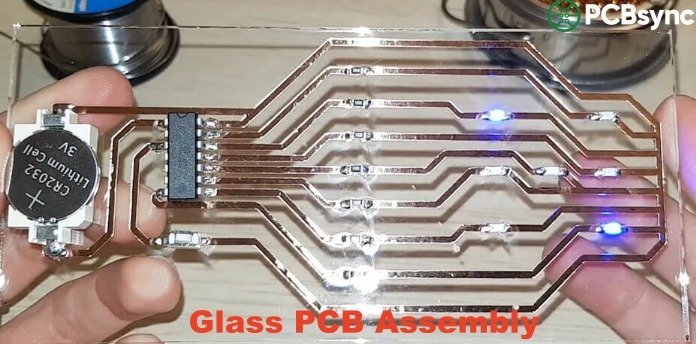
This represents the largest current application for glass PCBs. The combination of high thermal conductivity (for heat dissipation), transparency (for optical efficiency), and dimensional stability (for consistent light output) makes glass ideal for premium LED products. You’ll find glass substrates in digital billboards, automotive interior lighting, medical monitors, and architectural lighting where appearance matters.
5G and RF Communications
The rollout of 5G networks demands PCB materials that can handle higher frequencies with minimal signal loss. Glass substrates provide the stable dielectric properties and low loss tangent needed for base station components, antenna assemblies, and front-end modules. As 5G moves into mmWave frequencies, glass becomes increasingly attractive.
Automotive Electronics
Modern vehicles demand electronics that survive extreme temperature swings, vibration, and long service life. Glass PCBs appear in head-up displays, infotainment touch panels, LIDAR sensor assemblies, and power electronics. The CTE match with silicon helps ensure solder joint reliability over 15+ year vehicle lifespans.
Medical Devices
Biocompatibility, sterilization resistance, and optical clarity make glass substrates valuable for medical applications. You’ll find them in diagnostic imaging equipment, surgical lighting, implantable devices (using sapphire substrates), and precision laboratory instruments.
Consumer Electronics & Wearables
Smartwatches, AR glasses, and foldable smartphones increasingly use ultra-thin glass substrates. The technology enables bezel-less display designs, transparent electronic components, and compact form factors that consumers demand.
Application Summary Table
Industry
Key Applications
Glass Type Typically Used
LED & Display
Backlight units, digital signage, transparent displays
Manufacturing glass PCBs requires specialized processes that differ significantly from standard FR-4 fabrication. The workflows, equipment, and expertise needed represent a step change from conventional PCB production. Facilities that excel at FR-4 often struggle initially with glass—it’s genuinely a different discipline.
Here’s an overview of the key steps involved in glass PCB fabrication:
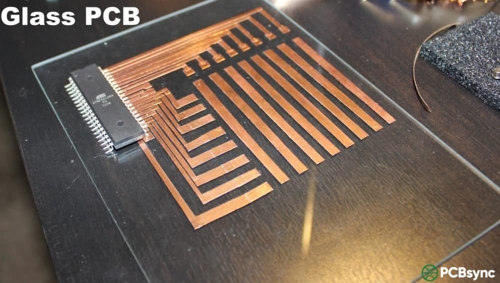
Substrate Preparation: Raw glass panels are precision-cut to size, then undergo ultrasonic or plasma cleaning to remove microscopic contaminants. Surface treatments improve adhesion for subsequent metallization.
Metallization: Thin copper or transparent conductive layers (ITO) are deposited onto the glass surface through sputtering, evaporation, or chemical plating processes.
Circuit Patterning: UV-curable photoresist is applied, exposed through a photomask containing the circuit pattern, then developed to create the etch mask. This process achieves finer line widths than conventional methods.
Etching: Unwanted metal is removed using chemical etchants (ferric chloride for copper), leaving the circuit traces behind.
Via Formation: Holes for interconnects are created using laser drilling rather than mechanical drilling (glass is too hard and brittle for standard drill bits).
Surface Finishing: Final protective coatings and surface finishes are applied. Clear solder masks preserve transparency where needed.
The specialized equipment and handling required for glass substrates contribute to their higher cost compared to FR-4. Breakage during PCB manufacturing remains a challenge—even small fractures render a panel unusable.
Quality control takes on added importance with glass PCBs. Every panel must be inspected for micro-cracks that could propagate during assembly or field use. Automated optical inspection systems detect defects that would be invisible to the naked eye. The scrap rate during early production runs can be significant until processes stabilize.
Assembly of glass PCBs also requires adaptation. Standard pick-and-place machines may need pressure adjustments to avoid cracking substrates. Reflow profiles must account for glass’s different thermal characteristics. Experienced contract manufacturers develop specific work instructions for glass substrate handling.
Considerations When Choosing Glass PCB
Glass PCBs aren’t the right choice for every application. Here’s what to weigh when deciding whether glass makes sense for your project:
Cost: Expect to pay 3-7x more than equivalent FR-4 boards. The premium is justified only when glass’s unique properties deliver clear benefits.
Lead Time: Fewer manufacturers work with glass substrates, and specialized processes take longer. Plan for extended lead times, especially for prototypes.
Fragility: Glass breaks. Assembly processes must be adapted, handling procedures established, and packaging designed to prevent damage.
Design Constraints: Complex board shapes with cutouts and notches increase breakage risk. Minimize stress concentrations in your design.
Layer Count: Most glass PCBs are single or double-layer. Multilayer glass construction is possible but adds significant complexity and cost.
Supplier Qualification: Verify that your manufacturer has genuine experience with glass substrates. Ask for samples and references before committing to production volumes.
Resources for Further Learning
Want to dive deeper into glass PCB technology? Here are valuable resources:
IPC Standards: IPC-4101 covers laminate specifications including glass substrates. Essential reading for design engineers.
IEEE Publications: Search IEEE Xplore for “glass substrate PCB” to find peer-reviewed research on advanced applications.
Material Supplier Datasheets: Companies like Corning, Schott, and AGC publish detailed specifications for their glass substrates.
PCB Manufacturer Application Notes: Leading glass PCB manufacturers often publish design guidelines specific to their processes.
Industry Conferences: Events like IPC APEX EXPO and SMTA International feature sessions on advanced substrate technologies.
Frequently Asked Questions
What is the main advantage of glass PCB over FR-4?
The most significant advantages are superior thermal conductivity (3-5x higher than FR-4), dimensional stability under heat, and the option for transparency. Glass also offers better CTE matching with silicon chips, which improves solder joint reliability. For applications requiring any of these properties, glass delivers performance that FR-4 simply cannot match.
How much does a glass PCB cost compared to standard PCB?
Glass PCBs typically cost 3-7 times more than equivalent FR-4 boards. The exact premium depends on glass type, board complexity, and order volume. Quartz and sapphire substrates command the highest prices, while tempered glass and borosilicate fall in the middle range. Factor in longer lead times and potential minimum order quantities when budgeting.
Can glass PCBs be used for high-frequency applications?
Yes, glass excels in high-frequency applications. Its stable dielectric constant and low dielectric loss make it well-suited for RF circuits, 5G components, and mmWave designs. Quartz glass in particular offers excellent high-frequency performance and is commonly used in radar and satellite communication systems.
Are glass PCBs suitable for flexible or bendable applications?
Ultra-thin glass substrates (under 0.2mm) can accommodate limited bending without breaking. However, glass will never match the flexibility of polyimide-based flex circuits. For applications requiring significant bending or dynamic flexing, traditional flex PCBs remain the better choice. Ultra-thin glass works best in “form-and-hold” applications like curved displays.
What industries benefit most from glass PCB technology?
LED lighting and display manufacturing currently represent the largest market for glass PCBs, followed by telecommunications (5G infrastructure), automotive electronics, and medical devices. Aerospace and defense applications also use glass substrates where extreme performance justifies the cost premium. Consumer electronics adoption is growing as transparent and foldable device designs become more common.
The Future of Glass PCB Technology
The glass PCB market continues evolving rapidly. Several trends are shaping where this technology heads next:
As 5G deployment accelerates globally, demand for high-frequency substrates will grow substantially. Glass’s stable dielectric properties position it well for millimeter-wave applications that standard materials struggle to support. The telecommunications infrastructure buildout represents a significant growth driver.
Electric vehicles present another expanding market. Battery management systems, power electronics, and advanced driver assistance systems all benefit from glass PCB characteristics. Automotive qualification requirements are demanding, but manufacturers achieving them gain access to high-volume, long-term programs.
Manufacturing costs should decrease as production scales and more fabricators develop glass substrate capabilities. While glass will likely never match FR-4 pricing, the premium should narrow over time—making glass viable for a broader range of applications.
Conclusion
Glass PCB technology offers compelling advantages for applications where thermal management, dimensional stability, high-frequency performance, or optical transparency matter. While the higher cost and manufacturing complexity limit glass to specialized applications today, the technology continues advancing as more manufacturers develop expertise and production scales up.
For engineers and designers working on next-generation electronics—whether that’s 5G infrastructure, advanced automotive systems, or innovative consumer devices—understanding glass PCB capabilities is becoming essential. The material won’t replace FR-4 for general-purpose applications, but it fills a critical niche where conventional substrates fall short.
The learning curve for designing with glass substrates is real but manageable. Start with lower-risk prototypes to build experience before committing critical programs. Work closely with your fabricator—their process knowledge often proves as valuable as the raw material properties.
When evaluating whether glass makes sense for your project, focus on the specific performance requirements rather than chasing the newest technology. If your design genuinely needs what glass provides, the premium is worthwhile. If not, proven materials remain the smarter choice.
Inquire: Call 0086-755-23203480, or reach out via the form below/your sales contact to discuss our design, manufacturing, and assembly capabilities.
Quote: Email your PCB files to Sales@pcbsync.com (Preferred for large files) or submit online. We will contact you promptly. Please ensure your email is correct.
Notes: For PCB fabrication, we require PCB design file in Gerber RS-274X format (most preferred), *.PCB/DDB (Protel, inform your program version) format or *.BRD (Eagle) format. For PCB assembly, we require PCB design file in above mentioned format, drilling file and BOM. Click to download BOM template To avoid file missing, please include all files into one folder and compress it into .zip or .rar format.


