Inquire: Call 0086-755-23203480, or reach out via the form below/your sales contact to discuss our design, manufacturing, and assembly capabilities.
Quote: Email your PCB files to Sales@pcbsync.com (Preferred for large files) or submit online. We will contact you promptly. Please ensure your email is correct.
Notes: For PCB fabrication, we require PCB design file in Gerber RS-274X format (most preferred), *.PCB/DDB (Protel, inform your program version) format or *.BRD (Eagle) format. For PCB assembly, we require PCB design file in above mentioned format, drilling file and BOM. Click to download BOM template To avoid file missing, please include all files into one folder and compress it into .zip or .rar format.
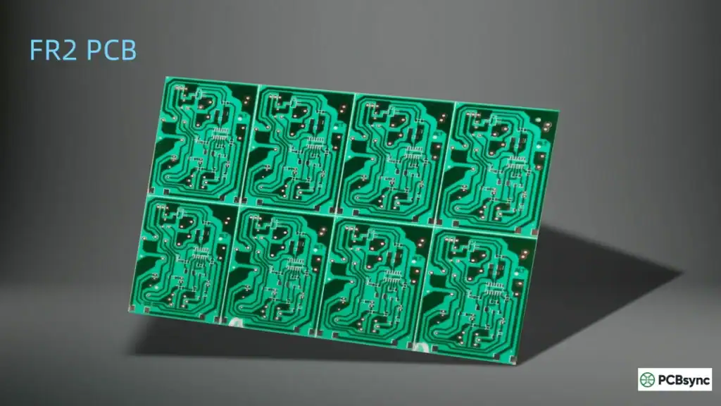
If you’ve been in the PCB industry for any length of time, you’ve probably come across FR2 material at some point. While FR4 dominates most conversations about circuit board substrates, FR2 holds its own in specific applications where cost efficiency is the primary concern. After working with various PCB materials over the years, I’ve found that understanding when to use FR2 versus other substrates can make a significant difference in both project budgets and product performance.
The history of FR2 dates back to the 1950s and 1960s when it emerged as an enhanced PCB substrate, utilizing cotton paper reinforced with phenolic resin. During that era, FR2 expanded PCB capabilities to meet the needs of industrial controls and instrumentation, including early aerospace applications. While technology has evolved significantly since then, FR2 still serves valuable purposes in modern electronics manufacturing.
In this comprehensive guide, I’ll walk you through everything you need to know about FR2 PCBs—from material composition and electrical properties to practical design considerations and real-world applications. Whether you’re designing low-cost consumer electronics or evaluating substrate options for a new project, this article will give you the technical foundation to make informed decisions.
FR2 stands for “Flame Retardant 2,” a NEMA designation for synthetic resin bonded paper used in printed circuit board manufacturing. The material consists of paper substrate (typically cotton paper or cellulose fibers) impregnated with plasticized phenol formaldehyde resin. This combination creates a rigid, flat laminate that provides adequate electrical insulation for many low-frequency applications.
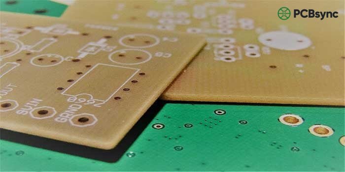
The phenolic resin composition falls into two categories: resoles and novolacs. Both work effectively for PCB applications, offering moisture resistance and good adhesion to copper foil. When you see an FR2 PCB, you’re looking at a brownish board that’s noticeably different from the green glass-epoxy appearance of FR4.
One key point about FR2: it’s compliant with the UL94V-0 standard, which is the benchmark for determining the flammability of plastic materials in electronics. This flame-retardant property is essential for meeting safety regulations in consumer products.
FR2 Material Composition and Structure
Understanding what goes into an FR2 board helps explain its performance characteristics. The base structure is relatively straightforward compared to more advanced substrates.
Core Components
The substrate uses paper reinforcement—specifically cellulose or cotton paper fibers—soaked in phenol-formaldehyde resin. This phenolic compound provides rigidity and some degree of moisture resistance. The paper base makes FR2 significantly lighter than glass-reinforced alternatives like FR4, coming in at approximately 15% lighter at equivalent thicknesses.
Copper foil is laminated onto one or both sides of the substrate, typically at 35 µm (1 oz/ft²) standard weight. For applications requiring higher current capacity, 50 µm copper is available. The thin copper layer can be etched or milled away to create the circuit traces needed for your design.
Flame Retardant Properties
The “FR” designation indicates that brominated flame retardants are incorporated into the resin system. Standard FR2 grades typically meet UL-94 HB (horizontal burn) requirements, though V-0 rated phenolic grades are available for applications requiring enhanced fire resistance. This is particularly important for power supplies and any equipment used in environments with fire risk.
Before specifying FR2 for any project, you need to understand its electrical, thermal, and mechanical characteristics. Here’s a breakdown of the critical specifications:
Property
FR2 Value
Notes
Dielectric Constant (Dk)
4.5 (typical)
Higher than FR4
Dissipation Factor
0.024 – 0.026
Signal loss factor
Dielectric Strength
~29 kV/mm
Good insulation
Glass Transition Temp (Tg)
105°C
Lower than FR4
Thermal Conductivity
~0.25 W/m·K
Limited heat spreading
Standard Thickness
1.2mm or 1.6mm
Thinner may warp
Copper Weight
35 µm (standard)
50 µm for higher current
Flammability Rating
UL94 HB / V-0
V-0 on request
A few things stand out from these specifications. The glass transition temperature of 105°C is notably lower than FR1’s 130°C and significantly below FR4’s typical 130-180°C range. This limits FR2’s suitability for lead-free soldering processes that typically require temperatures above 245°C. If you’re planning to use lead-free assembly, you’ll need to work carefully with your thermal profile.
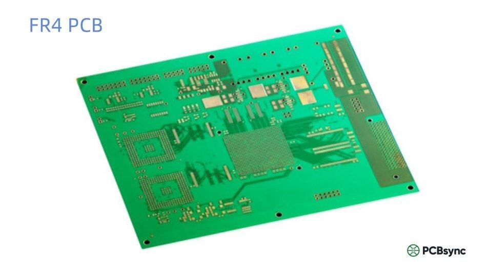
FR2 vs FR4: A Direct Comparison
This is probably the comparison most engineers want to see. Both materials serve as PCB substrates, but they’re designed for very different use cases. Here’s how they stack up:
Characteristic
FR2
FR4
Base Material
Paper/Cotton + Phenolic
Woven Fiberglass + Epoxy
Cost
~60% of FR4 cost
Standard pricing
Layer Support
Single-sided primarily
Up to 32+ layers
Through-Hole
Not recommended (PTH)
Excellent
Mechanical Strength
Lower rigidity
High strength
Thermal Performance
Tg: 105°C
Tg: 130-180°C
Frequency Range
Low frequency (<30 MHz)
Up to GHz range
Moisture Resistance
Fair (higher absorption)
Excellent (~0.10%)
Manufacturing
Punch-friendly, easy to cut
Requires routing/drilling
The cost difference is significant—FR2 runs about 60% of FR4 pricing, making it attractive for high-volume, cost-sensitive products. However, that savings comes with trade-offs in performance and design flexibility. FR4 dominates the industry (over 90% of rigid PCBs) for good reason: it handles everything from single-layer to complex multilayer designs with excellent electrical properties.
Common Applications for FR2 PCB
FR2 PCBs work best in applications where cost is the primary driver and performance requirements are modest. Here’s where you’ll typically find them:
Consumer Electronics
Remote controls and TV controllers
Basic calculators and digital clocks
Low-cost toys and electronic games
Simple household appliances
LED lighting fixtures
Basic audio equipment
Industrial and Power Applications
Simple power supplies and chargers
Electrical connectors and switches
Basic control panels
Solar cell controllers (non-critical)
Simple instrumentation
Prototyping and Education
FR2 is excellent for prototype work and educational purposes. It’s easy to solder, affordable enough for experiments, and works well for learning PCB assembly techniques. Many DIY electronics projects use FR2 boards because the material is forgiving and inexpensive to replace if something goes wrong.
Design Considerations for FR2 PCB
If you’re designing with FR2, there are several important constraints to keep in mind. Ignoring these can lead to manufacturing problems or field failures.
Layout Guidelines
Stick to single-layer designs: FR2 isn’t suitable for plated through-holes, so multilayer designs are essentially out. Plan your routing accordingly.
Use adequate pad sizes: Minimum 0.30mm for pads and annular rings. Square pads can help resist peel-off during thermal stress.
Design for punch manufacturing: FR2’s paper base makes it excellent for die-cutting, so take advantage of this for cost-effective outline and slot creation.
Allow for thermal relief: Use 4-spoke thermal relief patterns with spoke widths ≥0.30mm to prevent cold solder joints.
Maintain proper clearances: For 250V basic insulation, maintain 2.5mm creepage/clearance per IEC 60335-1.
Thermal Management
FR2’s thermal conductivity (0.25 W/m·K) limits heat spreading significantly compared to FR4 or metal-core alternatives. For components like TO-220 packages that generate heat, consider adding thick copper jumpers or external aluminum heat slugs. The board itself won’t dissipate heat effectively, so external thermal management is essential for any power application.
When designing power circuits on FR2, pay special attention to trace widths for current-carrying conductors. The general rule is to add 2mm of width per amp for traces carrying more than 2A. Wider traces help distribute heat more effectively across the limited thermal capacity of the paper substrate. Additionally, consider placing high-power components near the board edges where heat can dissipate more easily into the surrounding air.
Soldering and Component Mounting
This is critical: FR2 cannot withstand lead-free reflow temperatures (≥245°C). If you must use lead-free solder, stick to Sn-Pb wave or selective-solder profiles under 245°C. Heavy BGAs should be avoided entirely. The paper substrate will delaminate or blister under excessive thermal stress.
You have two primary mounting technology options for FR2 PCBs: Surface Mount Technology (SMT) and Through-Hole Mounting (THM). SMT works well for compact designs with surface mount devices, though you need to manage thermal profiles carefully. Through-hole components can be used, but remember that plated through-holes aren’t reliable on FR2. For through-hole work, you’re essentially soldering to pads on one side only, which affects mechanical strength of the solder joint.
Advantages and Limitations of FR2 PCB
Advantages
Advantage
Benefit
Low Cost
~40% savings vs FR4 for high-volume production
Easy Machining
Punch-friendly, burr-free edges, longer tool life
Lightweight
15% lighter than FR4 at same thickness
Good Insulation
Adequate dielectric strength for low-voltage applications
RoHS Compliant
Meets environmental regulations
Limitations
Limitation
Impact
Single-Layer Only
Cannot create complex multilayer designs
No PTH Support
Use wire jumpers, rivets, or solder bridges for crossovers
Lower Thermal Rating
Cannot withstand lead-free reflow (>245°C)
Higher Moisture Absorption
Not suitable for high-humidity environments
Frequency Limitations
Not recommended above ~30 MHz
Mechanical Weakness
Can crack under vibration; avoid automotive use
FR2 PCB Manufacturing Process
Understanding how FR2 boards are manufactured helps explain some of their characteristics and limitations.
Production Steps
Substrate Preparation: Paper substrate is impregnated with phenolic resin and cured to form the base laminate.
Copper Lamination: Copper foil is bonded to one or both sides under heat and pressure.
Circuit Imaging: Photoresist is applied and exposed to transfer the circuit pattern.
Etching: Unwanted copper is removed chemically to leave the circuit traces.
Surface Finish: HASL (Hot Air Solder Leveling) is commonly applied for solderable surfaces.
Punching/Cutting: Steel-rule punch dies cut board outlines, slots, and mounting holes.
Testing: Electrical testing verifies continuity and isolation.
The punching capability is a significant advantage for FR2. Unlike FR4, which requires routing or drilling for complex outlines, FR2 can be punched with steel-rule dies, dramatically reducing per-piece costs in high-volume production. This is one reason why FR2 remains popular for disposable consumer electronics despite its technical limitations.
Industry Standards and Compliance
When specifying FR2 for production, you should reference appropriate industry standards:
NEMA LI 1-1998: Defines FR-2 material properties and designations
IPC-4101 (/21 & /22): Laminate specifications for paper-reinforced phenolic materials
UL 94: Flammability testing (HB or V-0 ratings)
IPC-A-600: Acceptability criteria for printed boards
RoHS/REACH: Environmental compliance for hazardous substances
Useful Resources and References
For further reading and technical specifications, these resources are valuable:
IPC Standards: www.ipc.org – Official IPC standards documentation
NEMA Standards: www.nema.org – NEMA LI 1 material specifications
UL Standards: www.ul.com – UL 94 flammability certification
Wikipedia FR-2 Entry: en.wikipedia.org/wiki/FR-2 – General overview
PCB Material Databases: Manufacturer datasheets for specific FR2 laminate grades
Frequently Asked Questions About FR2 PCB
Can FR2 PCB be used for multilayer boards?
No, FR2 is not suitable for multilayer PCB construction. The material doesn’t support plated through-holes (PTH) reliably, which are essential for connecting layers in multilayer designs. FR2 works best for single-sided boards. For double-sided applications, you’ll need to use wire jumpers, rivets, or solder bridges for crossovers instead of traditional vias. If your design requires multiple layers, FR4 or similar glass-reinforced materials are the appropriate choice.
Is FR2 PCB compatible with lead-free soldering?
FR2 has limited compatibility with lead-free soldering processes. The material’s glass transition temperature of 105°C and its paper-based construction cannot withstand the typical lead-free reflow temperatures of 245°C and above. If you must use lead-free solder, wave soldering or selective soldering with profiles under 245°C can work, but you need to be careful with thermal management. Heavy components like BGAs should be avoided. For full lead-free compatibility, consider FR4 with higher Tg ratings.
What is the maximum operating frequency for FR2 PCB?
FR2 is recommended for low-frequency applications, typically below 30 MHz. The material’s higher dielectric constant (around 4.5) and dissipation factor cause greater signal loss at higher frequencies compared to FR4. For RF applications or high-speed digital circuits, the signal integrity issues become significant. If your application involves frequencies above 30 MHz, you should use FR4 or specialized high-frequency laminates like Rogers materials.
How much cheaper is FR2 compared to FR4?
FR2 typically costs about 60% of FR4 pricing, representing roughly 40% savings on material costs. However, the total cost picture depends on your production volume and manufacturing processes. FR2’s punch-friendly nature can add significant savings in high-volume production where die-cutting is faster than routing. But the limitation to single-layer designs and potential compatibility issues with modern assembly processes may offset some savings. For simple, high-volume products like remote controls or basic toys, FR2 offers meaningful cost advantages.
When should I choose FR2 over FR4 for my project?
Choose FR2 when your project meets these criteria: cost is the primary concern, the circuit is simple enough for single-layer design, operating frequency is below 30 MHz, power requirements are low to moderate, the product won’t be exposed to high humidity or extreme temperatures, and Sn-Pb soldering processes are acceptable. FR2 is ideal for disposable consumer electronics, educational projects, prototypes, and high-volume products where the savings justify the technical constraints. If any of these conditions aren’t met, FR4 is likely the better choice.
Conclusion
FR2 PCB occupies a specific niche in the electronics industry—one where cost efficiency outweighs performance requirements. For the right applications, it’s an excellent choice that can significantly reduce production costs while still delivering reliable functionality. The key is understanding its limitations and designing within them.
As a PCB engineer, I’ve used FR2 successfully in numerous cost-sensitive projects where the technical constraints weren’t limiting factors. Remote controls, simple LED controllers, basic power supplies—these are all applications where FR2 makes sense. But I’ve also seen projects fail when designers tried to push FR2 beyond its capabilities, particularly when attempting multilayer designs or high-frequency applications.
The material’s historical significance shouldn’t be overlooked either. FR2 helped enable the consumer electronics revolution of the latter 20th century, making affordable calculators, radios, and toys possible for mass markets. Even today, billions of FR2 boards are manufactured annually for products where cost-effectiveness is paramount.
The bottom line: know your requirements, understand the material’s properties, and make informed decisions. FR2 won’t replace FR4 as the industry standard, but it has its place. When the application fits, it’s a cost-effective solution that gets the job done reliably. Consider FR2 when designing high-volume, cost-sensitive products with simple circuit requirements, and you may find it’s exactly the right tool for the job.
Inquire: Call 0086-755-23203480, or reach out via the form below/your sales contact to discuss our design, manufacturing, and assembly capabilities.
Quote: Email your PCB files to Sales@pcbsync.com (Preferred for large files) or submit online. We will contact you promptly. Please ensure your email is correct.
Notes: For PCB fabrication, we require PCB design file in Gerber RS-274X format (most preferred), *.PCB/DDB (Protel, inform your program version) format or *.BRD (Eagle) format. For PCB assembly, we require PCB design file in above mentioned format, drilling file and BOM. Click to download BOM template To avoid file missing, please include all files into one folder and compress it into .zip or .rar format.


