Inquire: Call 0086-755-23203480, or reach out via the form below/your sales contact to discuss our design, manufacturing, and assembly capabilities.
Quote: Email your PCB files to Sales@pcbsync.com (Preferred for large files) or submit online. We will contact you promptly. Please ensure your email is correct.
Notes: For PCB fabrication, we require PCB design file in Gerber RS-274X format (most preferred), *.PCB/DDB (Protel, inform your program version) format or *.BRD (Eagle) format. For PCB assembly, we require PCB design file in above mentioned format, drilling file and BOM. Click to download BOM template To avoid file missing, please include all files into one folder and compress it into .zip or .rar format.
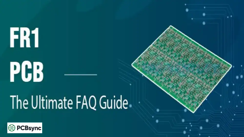
Looking for an affordable PCB substrate for your single-layer board project? FR1 PCB material offers excellent value for cost-sensitive electronics. This comprehensive guide covers everything you need to know about FR1 specifications, applications, and when to choose it over FR4.
What is FR1 PCB?
If you’ve been designing PCBs for any length of time, you’ve probably encountered the term FR1 at some point. FR1 PCB is a flame-retardant laminate material made from cellulose paper impregnated with phenol-formaldehyde (phenolic) resin. The “FR” designation stands for “Flame Retardant,” while the “1” indicates it’s the original formulation in this category of materials.
In practical terms, FR1 is a hard, flat material consisting of a paper-based substrate with a thin layer of copper bonded to one side. This creates what we call a copper-clad laminate—the foundation for etching circuit traces. The material meets IPC-4101 /21 & /22 specifications and conforms to UL94V-0 flammability standards.
I’ve worked with FR1 boards extensively in consumer electronics projects where cost was the primary driver. What makes this material particularly useful is its combination of adequate electrical properties and significantly lower cost compared to FR4. For single-layer PCB designs that don’t require through-hole plating or high-frequency performance, FR1 often makes more sense from a manufacturing economics standpoint.
Understanding the material composition helps explain why FR1 PCB behaves the way it does in various applications. The manufacturing process involves several key steps:
Paper Base Preparation
High-quality cellulose paper serves as the core material, providing the mechanical structure and thickness. This paper-based construction is fundamentally different from the woven fiberglass used in FR4, which explains many of the performance differences between these materials.
Phenolic Resin Impregnation
The paper is impregnated with phenol-formaldehyde resin, which provides flame retardancy and binding properties. This phenolic resin gives FR1 its characteristic brown color and contributes to its self-extinguishing behavior when exposed to flame.
Copper Foil Lamination
A thin copper foil (typically 1 oz or 35μm) is bonded to one side under heat and pressure. The result is a single-sided copper-clad laminate ready for circuit fabrication. The standard thickness ranges from 1.5mm to 1.6mm, roughly equivalent to two or three credit cards stacked together.
Before selecting any PCB material, you need hard numbers. Here’s the technical data for FR1 PCB that matters for design decisions:
Property
FR1 Value
Glass Transition Temperature (Tg)
130°C (266°F)
Dielectric Constant (Dk)
4.0 – 5.5 @ 1MHz
Flammability Rating
UL94 V-0
Standard Thickness
1.5mm – 1.6mm
Copper Weight
1 oz (35μm) typical
Maximum Operating Temperature
130°C
Moisture Absorption
Moderate to High
Thermal Conductivity
0.2 – 0.3 W/m·K
Comparative Tracking Index (CTI)
≥150V
Layer Configuration
Single-sided only
IPC Standard
IPC-4101 /21 & /22
FR1 vs FR2 vs FR3 vs FR4: Complete Comparison
One of the most common questions I get from junior engineers is about the differences between FR materials. Here’s the breakdown that actually matters for material selection:
Property
FR1
FR2
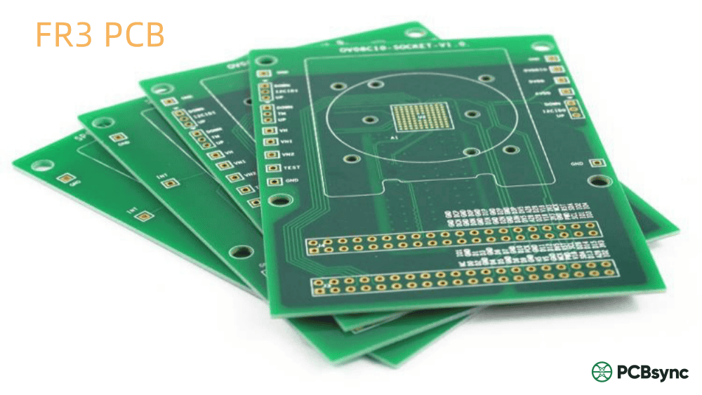
FR3
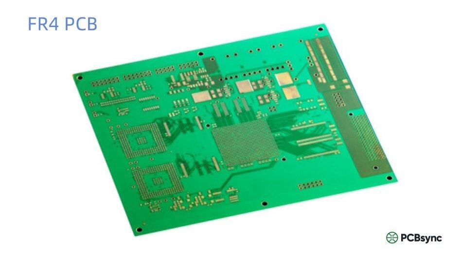
FR4
Base Material
Paper + Phenolic
Cotton Paper + Phenolic
Paper + Epoxy
Fiberglass + Epoxy
Tg (°C)
130
105
105-110
130-180
Cost (Relative)
Low ($)
Low ($)
Medium ($$)
Medium-High ($$$)
Layers Supported
Single
Single/Double
Single/Double
Multi-layer
Through-Hole
Poor
Poor
Fair
Excellent
High-Frequency
No
No
Limited
Yes
Moisture Resistance
Poor
Fair
Good
Excellent
Mechanical Strength
Low
Low-Medium
Medium
High
Pb-Free Soldering
No
No
Limited
Yes
Market Share
~5%
~3%
~2%
~90%
Key Takeaway: FR4 dominates because of its versatility, but FR1 PCB remains the go-to choice when you need the lowest possible material cost and your design is a simple single-layer board. The 60% cost savings compared to FR4 adds up quickly in high-volume production runs.
Advantages of FR1 PCB Material
Despite being the most basic FR-grade material, FR1 PCB offers several compelling advantages for the right applications:
Cost-Effective: Approximately 40-60% cheaper than FR4, making it ideal for budget-conscious projects and high-volume consumer goods.
Excellent Punchability: The paper core allows for die-cutting and punching without the fiberglass dust issues of FR4. Entire outlines, slots, and keyholes can be cut in milliseconds.
Lightweight: Paper core is approximately 15% lighter than FR4 at the same thickness.
Safe Machining: Unlike FR4 which produces hazardous glass-fiber dust when milled, FR1 can be machined with minimal safety concerns. Just keep debris away from eyes and lungs.
Simplified Design: Single-layer construction means straightforward routing without complex via strategies.
RoHS Compliant: Meets environmental regulations for restricted substances.
Flame Retardant: Self-extinguishing properties (UL94 V-0) provide safety in consumer applications.
Limitations and Constraints of FR1 PCB
Being honest about material limitations saves headaches down the road. Here’s where FR1 PCB falls short:
No Multilayer Support: Limited to single-sided configurations. If you need double-sided or multilayer, look elsewhere.
Poor Through-Hole Performance: The paper substrate doesn’t hold up well to drilling and plating processes.
Cannot Withstand Pb-Free Reflow: Peak temperatures of ≥245°C in lead-free soldering will damage the material. Use Sn-Pb wave soldering profiles <245°C.
Higher Dissipation Factor: Signal loss becomes significant above approximately 30MHz, making it unsuitable for RF or high-speed digital applications.
Moisture Sensitivity: Absorbs water in humid environments, causing swelling and Dk fluctuations. Not recommended for marine or outdoor applications.
Lower Mechanical Strength: Avoid mounting heavy components like transformers or using press-fit connectors.
Limited Temperature Range: Operating above 130°C will cause the board to soften and lose dimensional stability.
Best Applications for FR1 PCB
FR1 PCB shines in applications where cost matters more than performance margins. Based on real-world projects, here’s where this material makes the most sense:
If you’ve decided FR1 PCB is right for your project, here are practical design considerations:
Trace and Spacing Recommendations
Parameter
Minimum
Recommended
Trace Width
0.2mm (8 mil)
0.3mm+ (12 mil+)
Trace Spacing
0.2mm (8 mil)
0.3mm+ (12 mil+)
Pad Size (SMD)
0.4mm
0.5mm+
Drill Size
0.6mm
0.8mm+
Board Edge Clearance
0.3mm
0.5mm+
Soldering Process Considerations
Use Sn-Pb solder: Keep wave or selective solder profiles below 245°C.
Avoid BGA packages: Heavy components and lead-free reflow are not compatible with FR1.
Surface finish options: HASL (tin-lead), ENIG, and Immersion Silver all work with FR1.
Solder mask: Standard LPI solder mask can be applied for trace protection.
FR1 PCB Cost Analysis
Let’s talk numbers. The cost advantage of FR1 PCB becomes significant in volume production:
Factor
FR1
FR4
Raw Material Cost
~$0.90/sq ft
~$2.75/sq ft
Relative Cost
100% (baseline)
~300%
Processing
Simpler (punch/die-cut)
CNC routing required
Typical Scrap Rate
~3%
~0.5%
Best For
10,000+ units
All volumes
Pro Tip: For production runs exceeding 10,000 units with simple single-layer designs, the material cost savings with FR1 often justify any increase in handling or quality control overhead.
How to Specify FR1 PCB for Manufacturing
When ordering FR1 PCB from a manufacturer, include these specifications in your documentation:
Material: FR1 per IPC-4101/21 or /22
Thickness: 1.6mm (or specify)
Copper Weight: 1oz (35μm)
Surface Finish: HASL (Sn-Pb), ENIG, or Immersion Silver
Solder Mask: Green LPI (or specify color)
Silkscreen: White (single side)
Quality Standard: IPC-A-600 Class 2 (or Class 3 if required)
Useful Resources and Downloads
For deeper technical information on FR1 PCB and related standards, these resources are worth bookmarking:
Resource
Description / Link
IPC-4101 Standard
Base materials specification for rigid PCB laminates – Available from IPC (shop.ipc.org)
IPC-TM-650 Test Methods
Testing procedures for PCB materials – IPC Association
UL 94 Flammability Standards
Flame retardant classification reference – UL Standards
DigiKey Datasheets
FR1 product datasheets from Bantam Tools and others – digikey.com
IPC-A-600 Acceptability
Visual quality standards for PCB inspection – IPC
RoHS Directive
Environmental compliance requirements – EU regulations
Frequently Asked Questions About FR1 PCB
Can FR1 PCB be used for double-sided boards?
No. FR1 PCB is designed exclusively for single-sided applications. The paper-based substrate doesn’t support the through-hole plating process required for double-sided connectivity. If you need double-sided or multilayer boards, FR4 is the standard choice, though FR2 can work for simple double-sided designs with limited via requirements.
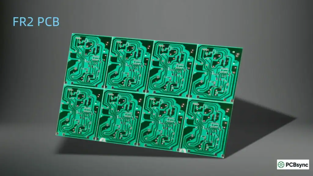
What’s the difference between FR1 and FR2?
The primary difference is glass transition temperature. FR1 has a Tg of 130°C while FR2 is rated at 105°C. Both use paper-phenolic construction, but FR2 uses cotton paper instead of cellulose. In practice, most manufacturers who produce FR1 don’t also produce FR2 since the materials have similar costs and applications. FR1 is generally preferred when available because of its higher temperature tolerance.
Is FR1 PCB RoHS compliant?
Yes, standard FR1 PCB materials meet RoHS 2 and REACH requirements. However, keep in mind that FR1 cannot withstand lead-free reflow soldering temperatures (≥245°C), so you’ll need to use Sn-Pb solder processes which have their own compliance considerations depending on your target market.
Can I mill FR1 PCB on a desktop CNC machine?
Absolutely. FR1 is actually preferred for desktop PCB milling because it doesn’t produce the hazardous glass-fiber dust that FR4 generates. Use 0.003″ or 0.005″ PCB engraving bits for trace isolation and 1/32″ flat end mills for holes and outlines. Make sure the board is completely flat and secured with double-sided tape—Nitto tape works best for holding the material during milling.
What surface finishes work with FR1 PCB?
FR1 PCB supports several surface finishes: HASL (Hot Air Solder Leveling) with tin-lead is most common and cost-effective. ENIG (Electroless Nickel Immersion Gold) works well for better solderability and shelf life. Immersion Silver provides good performance for mixed-signal applications. OSP (Organic Solderability Preservative) is also an option for short-term storage before assembly.
Conclusion
FR1 PCB material has been serving the electronics industry for decades, and it continues to be relevant for cost-sensitive, single-layer applications. While FR4 dominates the market at 90%+ share, FR1 fills an important niche where material cost directly impacts product viability.
The key is understanding where FR1 makes sense: simple consumer electronics, toys, basic chargers, LED lighting, and high-volume products where every fraction of a cent matters. Where it doesn’t make sense: anything requiring through-holes, multilayer stackups, high-frequency signals, lead-free soldering, or operation in harsh environments.
For your next project, evaluate the technical requirements honestly. If a single-layer board with basic electrical performance meets your needs, FR1 PCB could save 40-60% on material costs—money that might be better spent elsewhere in your BOM.
Inquire: Call 0086-755-23203480, or reach out via the form below/your sales contact to discuss our design, manufacturing, and assembly capabilities.
Quote: Email your PCB files to Sales@pcbsync.com (Preferred for large files) or submit online. We will contact you promptly. Please ensure your email is correct.
Notes: For PCB fabrication, we require PCB design file in Gerber RS-274X format (most preferred), *.PCB/DDB (Protel, inform your program version) format or *.BRD (Eagle) format. For PCB assembly, we require PCB design file in above mentioned format, drilling file and BOM. Click to download BOM template To avoid file missing, please include all files into one folder and compress it into .zip or .rar format.


