Inquire: Call 0086-755-23203480, or reach out via the form below/your sales contact to discuss our design, manufacturing, and assembly capabilities.
Quote: Email your PCB files to Sales@pcbsync.com (Preferred for large files) or submit online. We will contact you promptly. Please ensure your email is correct.
Notes: For PCB fabrication, we require PCB design file in Gerber RS-274X format (most preferred), *.PCB/DDB (Protel, inform your program version) format or *.BRD (Eagle) format. For PCB assembly, we require PCB design file in above mentioned format, drilling file and BOM. Click to download BOM template To avoid file missing, please include all files into one folder and compress it into .zip or .rar format.
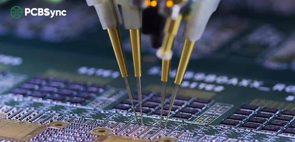
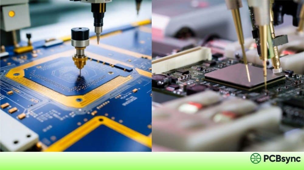
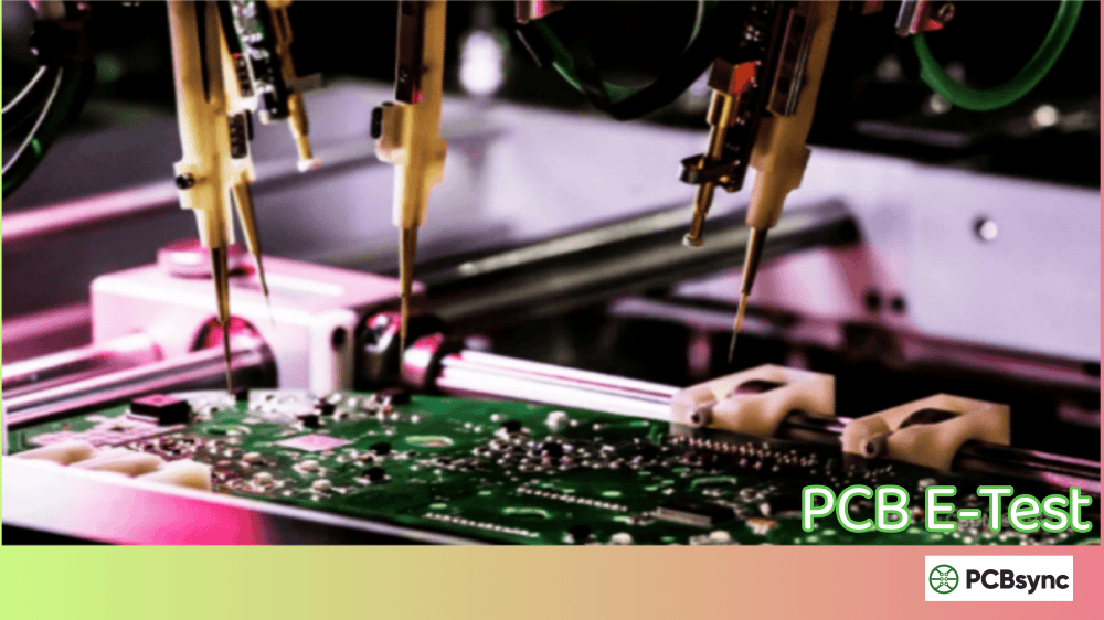
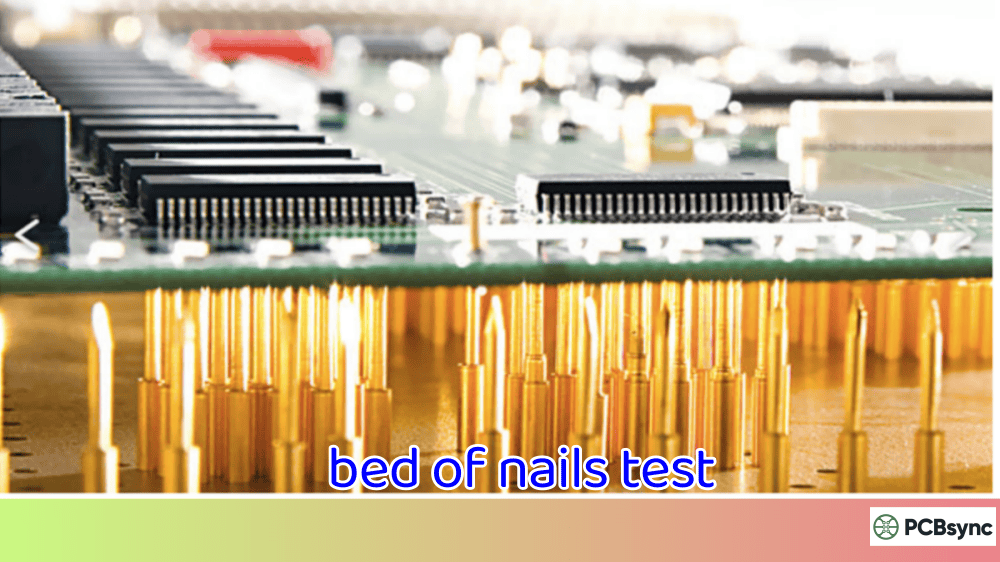
A flying probe test is an automated electrical testing method that uses movable probes—typically 2 to 8 needles—to make contact with test points on a printed circuit board. Unlike traditional bed-of-nails testing (ICT), these probes “fly” across the board surface, controlled by precision motors and software algorithms.
The concept emerged in the late 1980s as a response to a real problem: the high cost and long lead times associated with custom ICT fixtures. Back then, if you needed to test a new board design, you’d wait weeks for a dedicated fixture—and pay thousands of dollars for it. Flying probe testing eliminated that barrier.
The process is straightforward, though the technology behind it is sophisticated:
Program Generation: Test engineers feed CAD data (ODB++, IPC-2581, or Gerber files) along with the bill of materials into specialized software. The software generates probe paths and test sequences automatically.
Board Positioning: The PCB or PCBA is loaded onto a conveyor system and secured using mechanical fixtures, vacuum hold-down, or pneumatic clamps.
Probe Movement: High-precision motors move the probes in X, Y, and Z axes to contact test points—pads, vias, and component leads—according to the programmed sequence.
Measurement: At each contact point, the system injects test signals and measures electrical parameters. Results are compared against expected values in real-time.
Reporting: The system generates pass/fail reports with detailed diagnostics for any failures detected.
Modern flying probe testers can achieve positioning accuracy down to 10-15 micrometers, which matters when you’re testing boards with fine-pitch components or high-density interconnects.
What Can a Flying Probe Test Detect?
One question I get asked frequently is: “What exactly can this test catch?” Here’s a comprehensive breakdown:
Defect Type
Detection Method
Typical Application
Open circuits
Continuity measurement
Broken traces, cold solder joints
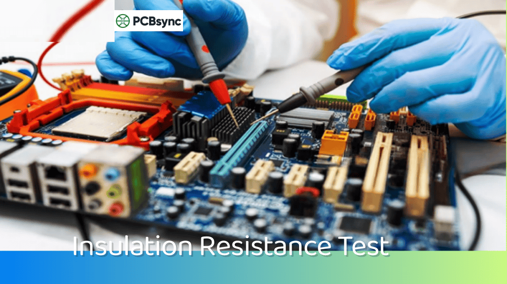
Short circuits
Isolation measurement
Solder bridges, copper debris
Resistance values
Ohmic measurement
Resistor verification
Capacitance values
Capacitive measurement
Capacitor verification
Inductance values
Inductive measurement
Inductor verification
Diode orientation
Forward/reverse bias test
Polarity verification
Component presence
Signature analysis
Missing components
Wrong component
Value comparison
Assembly errors
Micro-shorts
High-voltage stress test
Contamination, whiskers
Beyond these standard tests, advanced flying probe systems can perform:
Boundary scan testing via JTAG interface
LED verification with optical sensors for color and polarity
IC programming during the test sequence
Thermal scanning for detecting abnormal heat signatures
Flying Probe Test for PCB vs. PCBA: Key Differences
This is where things get interesting. Flying probe testing serves two distinct purposes depending on when it’s applied in the manufacturing process.
Bare PCB Testing (Pre-Assembly)
When testing bare boards before component assembly, the focus is entirely on the substrate integrity:
Trace continuity across all layers
Via connectivity (through-hole, blind, and buried vias)
Isolation between adjacent nets
Impedance verification for controlled-impedance designs
Detection of copper defects, opens, and shorts
At this stage, probes have full access to all pads and vias since no components obstruct the surface.
PCBA Testing (Post-Assembly)
Testing assembled boards adds complexity but provides comprehensive quality verification:
All bare board tests plus component verification
Solder joint integrity assessment
Component value and orientation checks
Basic functional verification where accessible
The challenge with PCBA testing is accessibility. Ball grid arrays (BGAs), chip-scale packages, and 0201 components leave minimal probe access. Good design-for-test (DFT) practices become critical here.
Comparison: PCB vs. PCBA Flying Probe Testing
Aspect
Bare PCB Testing
PCBA Testing
Primary Focus
Board integrity, trace connectivity
Component + board verification
Timing
After fabrication, before assembly
After component assembly
Test Coverage
Typically 95-100% net access
70-95% depending on design
Test Speed
Generally faster
Slower due to complexity
Probe Access
Full access to all test points
Limited by component placement
Defects Detected
Fabrication defects
Fabrication + assembly defects
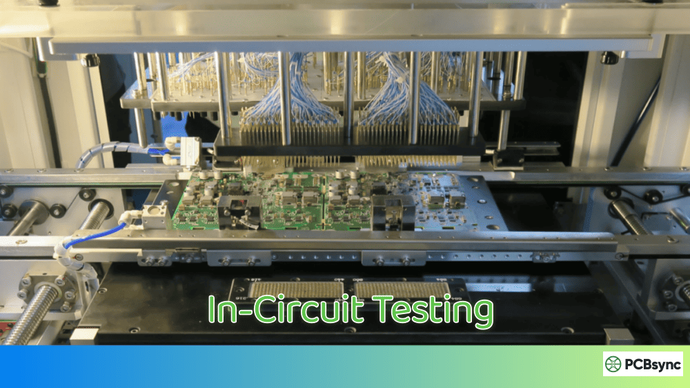
Flying Probe Test vs. In-Circuit Test (ICT): Making the Right Choice
This comparison comes up in virtually every test strategy discussion. Both methods have their place, and understanding when to use each can save significant time and money.
Flying Probe Test Advantages
No fixture cost: Eliminates $3,000-$20,000+ fixture investment
Fast setup: Test programs ready in hours to days, not weeks
BGA challenges: Limited access to hidden solder joints
Cost Comparison: Flying Probe vs. ICT
Cost Factor
Flying Probe Test
In-Circuit Test (ICT)
Fixture Cost
$0
$3,000-$20,000+
Programming Cost
$500-$2,000
$1,000-$3,000
Setup Time
Hours to days
2-6 weeks
Test Time per Board
5-15 minutes
30-60 seconds
Design Change Cost
Program update only
Fixture modification + program
Break-even Volume
Best under 500-1,000 units
Best over 1,000-5,000 units
The rule of thumb I follow: if you’re producing fewer than 500 boards or expect design revisions, flying probe testing almost always makes more economic sense. For stable, high-volume production, ICT wins on throughput and per-unit cost.
Design Guidelines for Optimal Flying Probe Testing
Here’s where practical experience really pays off. Following these guidelines during the design phase will dramatically improve test coverage and reduce testing time.
Test Point Requirements
Parameter
Minimum
Recommended
Test pad diameter
6 mil (0.15mm)
20 mil (0.5mm)
Via diameter
8 mil (0.2mm)
10-12 mil (0.25-0.3mm)
Test point spacing
10 mil (0.25mm)
20 mil (0.5mm)
Pad-to-component clearance
8 mil (0.2mm)
12 mil (0.3mm)
Board Layout Considerations
Border Edge Requirements: Leave at least 6mm (0.24″) clear on opposite edges of the board for machine handling. This can be panel waste or designed into the board itself.
Fiducial Markers: Include at least 3 fiducials (2 diagonal) for probe positioning accuracy. Place these on the PCB itself when possible, not just on panel waste.
Via Design: Keep vias non-tented (solder mask open) if you plan to probe them. Tented vias work, but exposed vias provide more reliable contact.
Component Height: Keep component heights under 40mm on the probing side. Taller components create “no-fly zones” that restrict probe access.
Test Point Clustering: Group test points to minimize probe travel time. On large boards, this optimization can reduce test time by 20-30%.
SMD Component Considerations
For surface-mount devices, especially fine-pitch components:
Extend solder pads by 12 mil (0.3mm) beyond component leads where possible
Never probe directly on component pins—target the pad extension
For BGAs and QFNs, route critical nets to accessible vias or test points
The Flying Probe Testing Process: Step by Step
Let me walk you through a typical flying probe test workflow from an engineer’s perspective.
Step 1: Data Preparation
Gather these files before approaching your test house:
CAD Data: ODB++ format is preferred; IPC-2581 and native ECAD formats also work well. Gerber files can be used but require more manual setup.
Bill of Materials (BOM): Excel format with component values, tolerances, and reference designators
Netlist: Extracted from your EDA tool
Assembly Drawings: For component placement reference
Step 2: Test Program Development
The test engineering team will:
Import design data into the flying probe software
Identify all nets and assign test points
Generate optimal probe paths (the software handles this automatically)
Set measurement parameters for each component type
Define pass/fail thresholds based on BOM tolerances
For a moderately complex board, expect program development to take 4-8 hours.
Step 3: Debug and Validation
Before production testing begins:
Run the program on known-good boards to establish baselines
Adjust probe positions for reliable contact
Fine-tune measurement parameters to eliminate false failures
Verify all critical nets have coverage
Step 4: Production Testing
During actual production:
Boards are loaded automatically or manually
Test sequence executes per the program
Real-time results display pass/fail status
Failed boards are marked and set aside for diagnosis
Statistical data is collected for SPC analysis
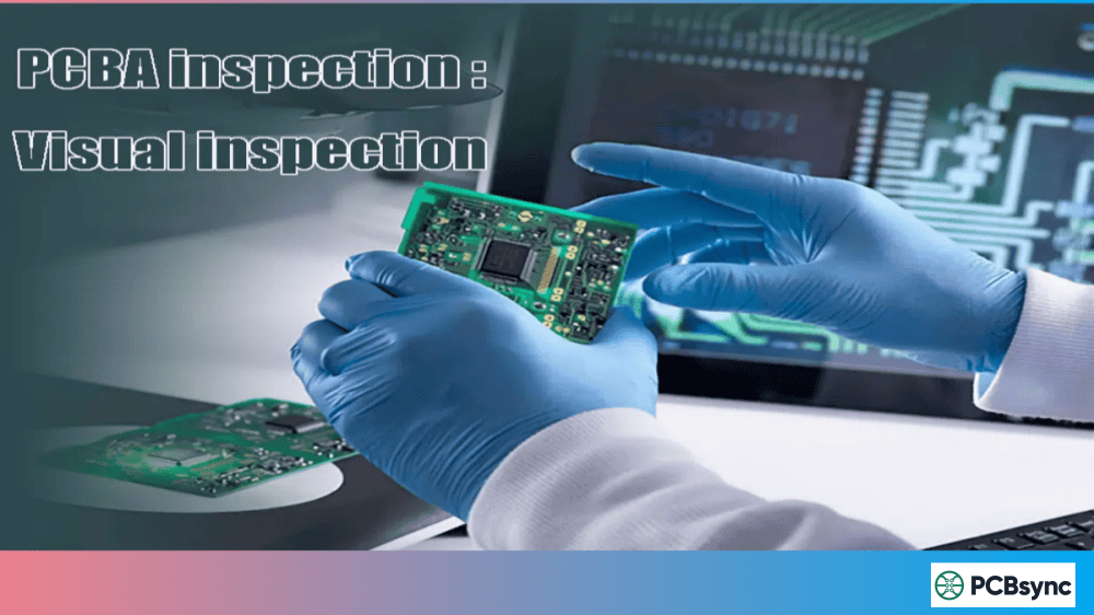
Integrating Flying Probe Test with Other Inspection Methods
Flying probe testing rarely stands alone in a comprehensive quality program. Here’s how it fits with other inspection methods:
Recommended Test Flow
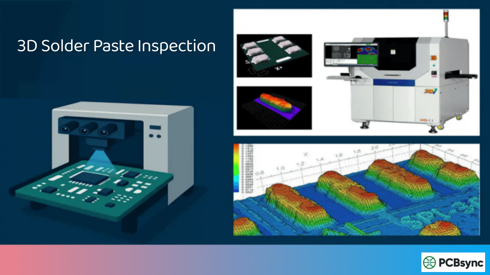
Bare PCB Fabrication ↓ Flying Probe Test (Bare Board) ↓ SMT Assembly ↓ Solder Paste Inspection (SPI) ↓ Automated Optical Inspection (AOI) ↓ Flying Probe Test (PCBA) or ICT ↓ Functional Test ↓ Final QC
Complementary Methods
Method
What It Catches
Pairs Well With FPT
AOI
Placement errors, solder defects
Yes—visual complements electrical
X-ray
Hidden solder joints (BGA, QFN)
Yes—covers FPT blind spots
SPI
Solder paste volume/position
Yes—prevents assembly defects
Functional Test
System-level operation
Yes—FPT catches component-level issues
Burn-in
Infant mortality failures
Sometimes—depends on application
The combination of AOI plus flying probe testing provides coverage exceeding 95% for most board designs.
Acculogic (Canada) — Combined FPT and ICT solutions
ATG Luther & Maelzer (Germany) — Bare board testing specialists
IPC Class Requirements for Testing
IPC Class
Application
Typical Test Requirements
Class 1
Consumer electronics
Basic continuity, isolation
Class 2
Industrial, telecom
Standard 100V isolation, 10Ω continuity
Class 3
High-reliability, aerospace
250V isolation, 100MΩ minimum
Class 3/A
Military avionics
250VDC, 100MΩ isolation, 10Ω continuity
When to Choose Flying Probe Testing
Based on years of practical experience, here’s my decision framework:
Choose Flying Probe Test When:
Production volume is under 500-1,000 units
You’re in the prototype or NPI phase
Design changes are expected or frequent
Time-to-market is critical
Fixture costs aren’t justifiable
Board designs are highly complex or dense
You need quick turnaround (days, not weeks)
Consider Alternatives When:
Production exceeds 5,000+ units with stable design
Test time per board must be under 1-2 minutes
Complex functional testing is required
Budget allows for fixture investment with long-term payoff
Frequently Asked Questions About Flying Probe Testing
What files do I need to provide for flying probe testing?
You’ll need three essential items: CAD data in ODB++ format (preferred), IPC-2581, or native ECAD files; a bill of materials in Excel format with component values and tolerances; and Gerber files with drill data if ODB++ isn’t available. Most test houses can work with various formats, but ODB++ provides the cleanest data import and fastest program generation.
How long does a flying probe test take per board?
Test time depends on board complexity, but typically ranges from 5 to 15 minutes per board. Simple boards with fewer test points can complete in 3-5 minutes, while complex multilayer boards with thousands of nets may take 20-30 minutes. This is significantly slower than ICT (which tests in under 1 minute) but the tradeoff is zero fixture cost and immediate availability.
Can flying probe testing detect BGA solder defects?
Flying probe testing has limited ability to directly test BGA solder joints since the connections are hidden beneath the component. However, the test can verify net connectivity through accessible vias or test points connected to BGA pins. For comprehensive BGA inspection, pair flying probe testing with X-ray inspection, which can visualize hidden solder joints directly.
What is the minimum pad size for flying probe testing?
Most modern flying probe systems can reliably contact pads as small as 6 mil (0.15mm), though 20 mil (0.5mm) is recommended for optimal contact reliability. Some advanced systems, like SPEA testers, can contact micro-pads down to 50 micrometers on PCBs and 20 micrometers on wafers. Always confirm capabilities with your test service provider based on your specific design.
Is flying probe testing suitable for high-volume production?
Flying probe testing is generally not cost-effective for high-volume production (typically over 5,000+ units) due to longer test times per board. For high-volume runs, ICT with custom fixtures provides faster throughput and lower per-unit test costs. However, some manufacturers use flying probe testing even at higher volumes when design stability is uncertain or when the cost of fixture modifications outweighs the slower test time.
Flying Probe Test Equipment: Understanding System Configurations
Not all flying probe testers are created equal. Understanding the different configurations helps you choose the right equipment or evaluate test service providers.
Single-Sided vs. Double-Sided Systems
Single-sided flying probe systems position probes on only one side of the board at a time. These systems are more affordable and work well for simpler designs with most test points on one surface. However, testing both sides requires flipping the board and running a second test cycle, which increases handling time.
Double-sided flying probe systems deploy probes simultaneously on top and bottom surfaces. This configuration dramatically reduces test time for complex boards with components and test points on both sides. Modern double-sided systems like the Seica Pilot V8 can probe both surfaces simultaneously while accommodating components up to 40mm high on each side.
Horizontal vs. Vertical Architectures
Horizontal systems position the board flat during testing. This configuration suits most applications and allows easier integration with automated handling systems.
Vertical systems hold the board upright during testing. This architecture saves floor space and can handle larger, heavier boards more effectively. Some manufacturers prefer vertical systems for testing large backplanes or panel arrays.
Number of Probes and Speed Impact
Flying probe systems range from basic 4-probe configurations to advanced 20-probe systems:
Probe Configuration
Typical Application
Relative Speed
4 probes (single-sided)
Simple boards, prototypes
Slowest
6-8 probes (double-sided)
Standard PCBA testing
Moderate
12-16 probes
Complex boards, medium volume
Fast
20+ probes
High-complexity, higher volume
Fastest
More probes enable parallel testing of multiple points, reducing overall test time significantly.
Common Flying Probe Test Challenges and Solutions
Even with a well-designed test program, certain challenges arise during flying probe testing. Here’s how experienced test engineers address them.
Challenge 1: Probe Marks on Pads
Problem: Flying probes can leave small indentations or marks on test pads, which some customers consider cosmetic defects.
Solution: Modern flying probe systems incorporate “soft touch” technology that limits contact force. Additionally, specifying probe landing on non-critical pads or vias rather than primary solder pads minimizes cosmetic concerns. Some advanced systems achieve zero-force landing for sensitive applications.
Challenge 2: Accessing Dense Component Areas
Problem: High-density boards with minimal spacing between components leave little room for probe access.
Solution: Plan test point access during schematic capture and layout phases. Route critical nets to accessible vias or dedicated test pads. For unavoidable blind spots, combine flying probe testing with complementary methods like boundary scan or X-ray inspection.
Challenge 3: False Failures from Flux Residue
Problem: Flux residue or contamination on test points causes intermittent contact failures, triggering false rejects.
Solution: Specify no-clean flux processes compatible with electrical testing, or implement board cleaning before testing. Alternatively, use flying probe systems with automated probe cleaning features that wipe probes between contacts.
Challenge 4: Long Test Times on Large Boards
Problem: Large boards with thousands of nets can take 30+ minutes to test, creating production bottlenecks.
Solution: Optimize probe path algorithms for efficiency (modern software does this automatically). Group test points to minimize travel distance. For critical throughput requirements, consider panel testing multiple small boards simultaneously.
Challenge 5: Testing High-Frequency Circuits
Problem: Standard flying probe measurements may not accurately characterize high-frequency signal paths.
Solution: For RF and high-speed digital designs, use specialized flying probe systems with impedance measurement capabilities. Alternatively, combine flying probe testing with dedicated impedance testing for controlled-impedance traces.
Advanced Flying Probe Test Capabilities
Beyond basic continuity and component verification, modern flying probe systems offer advanced capabilities that expand testing possibilities.
Boundary Scan (JTAG) Integration
Many flying probe systems integrate JTAG boundary scan capability. This enables testing of components that would otherwise be inaccessible to physical probes—particularly useful for verifying BGA connections and testing complex digital ICs.
The flying probes contact JTAG interface points (TDI, TDO, TMS, TCK, TRST) while the system executes boundary scan test patterns. This combination provides coverage that neither method achieves alone.
LED Testing with Optical Sensors
For boards with indicator LEDs, advanced flying probe systems include optical sensors that verify LED function, color, and intensity. The probes power the LED while optical sensors confirm proper operation—catching polarity errors, wrong-value resistors in LED circuits, and defective LEDs themselves.
High-Voltage Stress Testing
Standard continuity tests may not detect marginal defects like micro-shorts or contamination between traces. High-voltage stress (HVS) testing applies elevated voltages (typically 250V-1000V) to detect these subtle faults before they cause field failures.
HVS testing is particularly valuable for:
Automotive electronics operating in harsh environments
Power supply circuits with high-voltage traces
Medical devices requiring long-term reliability
Aerospace applications with stringent quality requirements
Thermal Scanning
Some advanced flying probe systems incorporate thermal imaging to detect abnormal heat signatures during powered testing. Hot spots can indicate shorted components, incorrect values causing excessive current, or poor solder joints with elevated resistance.
Industry Applications for Flying Probe Testing
Flying probe testing serves diverse industries, each with specific requirements and challenges.
Automotive Electronics
Automotive applications demand high reliability in harsh environments. Flying probe testing verifies board integrity before costly assembly into vehicle systems. Many automotive suppliers combine flying probe testing with 100% AOI and sample-based X-ray inspection to meet IATF 16949 quality requirements.
Medical Devices
Medical electronics require extensive documentation and traceability. Flying probe testing generates detailed test reports that support FDA submissions and quality system compliance. The fixtureless nature of flying probe testing also accommodates the frequent design iterations common in medical device development.
Aerospace and Defense
Military and aerospace applications typically specify IPC Class 3 or Class 3/A requirements with more stringent electrical test parameters. Flying probe testing meets these demands while providing the flexibility needed for low-volume, high-mix production typical in defense manufacturing.
Consumer Electronics
While high-volume consumer products often use ICT for production testing, flying probe testing plays a crucial role during prototype development and new product introduction. The rapid program turnaround helps consumer electronics companies meet aggressive launch schedules.
Industrial and Telecommunications Equipment
Industrial equipment and telecom infrastructure often involve complex, high-layer-count boards with mixed technologies. Flying probe testing’s ability to handle diverse board types without dedicated fixtures makes it ideal for the varied product mix common in these industries.
Cost-Benefit Analysis: Making the Business Case
When presenting flying probe testing to management or customers, a clear cost-benefit analysis helps justify the approach.
Direct Cost Savings Example
For a typical prototype run of 50 boards:
Cost Factor
ICT Approach
Flying Probe Approach
Fixture cost
$8,000
$0
Programming
$2,000
$1,000
Lead time
4 weeks
3 days
Test cost ($10/board)
$500
$500
Total
$10,500
$1,500
The savings become less dramatic at higher volumes, but the break-even point typically falls between 500-2,000 units depending on board complexity and fixture costs.
Indirect Benefits Worth Considering
Beyond direct cost savings, flying probe testing provides:
Faster time-to-market: Days instead of weeks for test setup
Flexibility: Same equipment tests multiple board designs
Final Thoughts
Flying probe testing has earned its place as a go-to solution for PCB and PCBA quality assurance, particularly in the prototype-to-production transition phase where flexibility and speed matter more than raw throughput.
The technology continues to evolve—modern systems offer faster probe movement, better precision, and integrated capabilities like boundary scan and optical inspection. For engineers and manufacturers dealing with complex boards, tight schedules, and uncertain design stability, flying probe testing provides the balance of coverage, cost, and convenience that traditional fixture-based testing simply can’t match.
The key is understanding where it fits in your test strategy. Used appropriately—as part of a comprehensive quality program that includes AOI, X-ray where needed, and functional testing—flying probe testing helps catch defects early, reduces rework costs, and ultimately delivers more reliable products to your customers.
Whether you’re a design engineer planning for testability, a manufacturing engineer selecting test methods, or a quality manager building a comprehensive inspection strategy, flying probe testing offers capabilities that address real-world production challenges. The investment in understanding this technology pays dividends throughout your product lifecycle.
Inquire: Call 0086-755-23203480, or reach out via the form below/your sales contact to discuss our design, manufacturing, and assembly capabilities.
Quote: Email your PCB files to Sales@pcbsync.com (Preferred for large files) or submit online. We will contact you promptly. Please ensure your email is correct.
Notes: For PCB fabrication, we require PCB design file in Gerber RS-274X format (most preferred), *.PCB/DDB (Protel, inform your program version) format or *.BRD (Eagle) format. For PCB assembly, we require PCB design file in above mentioned format, drilling file and BOM. Click to download BOM template To avoid file missing, please include all files into one folder and compress it into .zip or .rar format.


