Contact Sales & After-Sales Service

Contact & Quotation

  • Inquire: Call 0086-755-23203480, or reach out via the form below/your sales contact to discuss our design, manufacturing, and assembly capabilities.
  • Quote: Email your PCB files to Sales@pcbsync.com (Preferred for large files) or submit online. We will contact you promptly. Please ensure your email is correct.
Drag & Drop Files, Choose Files to Upload You can upload up to 3 files.

Notes:
For PCB fabrication, we require PCB design file in Gerber RS-274X format (most preferred), *.PCB/DDB (Protel, inform your program version) format or *.BRD (Eagle) format. For PCB assembly, we require PCB design file in above mentioned format, drilling file and BOM. Click to download BOM template To avoid file missing, please include all files into one folder and compress it into .zip or .rar format.

Flexible PCB Manufacturing

As a trusted flexible PCB manufacturer, we provide end-to-end manufacturing services backed by rigorous quality control and expedited lead times to keep your projects on track.

Try fitting a traditional printed circuit board inside a smartwatch. Or getting one to survive the constant opening and closing of a laptop hinge. It’s not happening. Rigid PCBs have served us well for decades, but they hit a wall when you need circuits that actually bend, twist, or fit into tight spaces.

That’s the whole point of flexible printed circuit boards (flex PCBs). They’re exactly what they sound like—circuit boards you can bend. But there’s a lot more to them than just being bendy versions of regular PCBs. The materials are different, the design rules change completely, and if you don’t know what you’re doing, you’ll end up with circuits that crack, connections that fail, or costs that spiral out of control.

This guide covers what you actually need to know if you’re working with flex PCBs. We’ll start with the basics—what they are, how they work, and when you should use them instead of

 rigid boards. Then we’ll get into the details: materials, design rules, manufacturing, costs, and the mistakes people make (so you don’t have to).

If you’re designing your first flex circuit, trying to decide between flex and rigid for a project, or just want to understand why your phone’s display connector looks the way it does, you’re in the right place.

Flexible PCB Calculator & Design Tool | PCBsync Engineering Tools

Flexible PCB Calculator & Design Tool

PCBsync Engineering Tools

Bend Radius Calculator (IPC-2223)

Total Flex Thickness --
IPC Bend Ratio (r/h) --
Minimum Bend Radius --
Recommended (+20% safety) --
Expected Flex Life --

IPC-2223 Bend Radius Guidelines

Quick Tip

For dynamic applications, always use RA copper and minimize thickness. Thinner = tighter bends + longer flex life.

Bend Ratio Table (IPC-2223)

ApplicationLayersRatio (r/h)
Static1-26:1
Static3+12:1
Dynamic1100:1
Dynamic2150:1
Dynamic3+200:1

Design Warnings

  • Never place vias in bend areas
  • Route traces perpendicular to bend axis
  • Use hatched ground planes in flex zones
  • ED copper NOT recommended for dynamic
  • Add 20% safety margin to calculations

Stack-Up Configuration

Stack-Up Visualization

Total Flex Thickness 0.11 mm
With Stiffener 0.11 mm
Min Bend Radius (static) 0.66 mm

Flexible PCB Material Comparison

Selection Guide

Choose Polyimide (PI) for most applications. PET for low-cost/low-temp only. LCP for high-frequency/harsh environments.

Polyimide (PI)

Temp Range-269°C to +400°C
Dk3.2 - 3.5
Df0.002 - 0.003
Moisture2-3%
Cost1.0x
UseMost Apps

Polyester (PET)

Temp Range-40°C to +105°C
Dk3.0 - 3.2
Df0.005 - 0.020
Moisture<0.4%
Cost0.3-0.5x
UseLow-Cost

LCP

Temp Range-40°C to +280°C
Dk2.9 - 3.0
Df0.002 - 0.004
Moisture<0.04%
Cost2-3x
UseRF/5G

Copper Foil: RA vs ED

PropertyRA CopperED Copper
GrainHorizontalColumnar
Elongation20-45%4-10%
Flex LifeExcellentLimited
Cost+20-30%Baseline
Best ForDynamic FlexStatic Flex

Coverlay vs Flex Solder Mask

PropertyPI CoverlayFlex Mask
MaterialPolyimide filmPhoto-imageable
FlexibilityExcellentGood
Opening Tol.±0.15mm±0.05mm
Dynamic FlexRequiredNo
CostHigherLower

Flexible PCB Cost Estimator

×

Cost Breakdown

Material
$45
Manufacturing
$52
Surface Finish
$18
Testing & QC
$12

Estimated Total

$127

$1.27 per unit

Note

Rough estimate only. Contact PCBsync for accurate quotes.

Flex PCB Design Rules

ParameterStandardAdvanced
Min Trace Width0.1mm (4mil)0.05mm (2mil)
Min Spacing0.1mm (4mil)0.05mm (2mil)
Min Drill0.2mm0.1mm
Annular Ring0.15mm0.1mm
Coverlay Opening±0.15mm±0.1mm
Registration±0.1mm±0.05mm
Impedance Tol.±10%±5%

Routing Guidelines

DO

  • Route traces perpendicular to bend
  • Use curved traces (no sharp corners)
  • Distribute traces evenly
  • Use hatched ground planes
  • Add teardrop pad entries

DON'T

  • Place vias in bend areas
  • Route parallel to bend axis
  • Use 90° corners
  • Use solid copper pours in flex
  • Place components near flex edge

IPC Standards Reference

StandardTitleApplication
IPC-2223Sectional Design Standard for FPBsPrimary design guide
IPC-6013Performance Specification for FPBsAcceptance criteria
IPC-4202Flexible Base DielectricsMaterial specs
IPC-4203Cover Sheets SpecificationCoverlay specs
IPC-A-600Acceptability of Printed BoardsVisual standards

Unit Conversions

LengthConversion
1 mil= 25.4 μm = 0.001 inch
1 μm= 0.0394 mil
1 mm= 39.37 mil = 1000 μm
Copper WeightThickness
1/4 oz9 μm (0.35 mil)
1/3 oz12 μm (0.47 mil)
1/2 oz18 μm (0.7 mil)
1 oz35 μm (1.4 mil)
2 oz70 μm (2.8 mil)

PI Temp Limit

+400°C

Survives lead-free reflow (260°C)

Dielectric (PI)

Dk 3.2-3.5

At 1 MHz frequency

Dynamic Life

1M+ cycles

With RA copper + proper design

Min Thickness

~0.08mm

Single-layer with thin materials

Moisture (PI)

2-3%

Bake 120°C/4hrs before solder

Elongation

RA: 20-45%

vs ED copper 4-10%

What Is a Flexible PCB?

Definition & Basic Structure

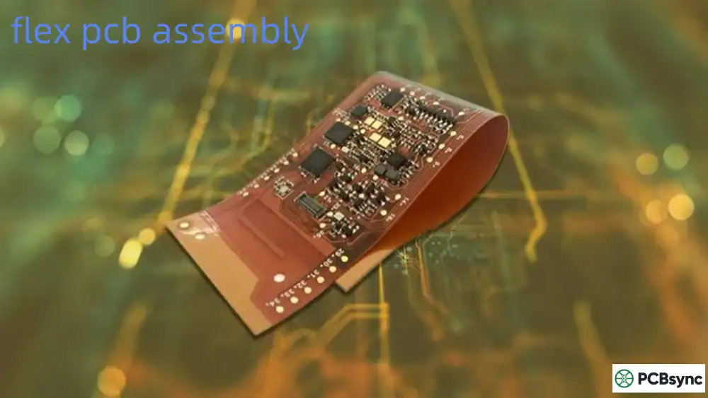
A flexible printed circuit board (flex PCB or FPC) is a type of circuit board designed to bend, fold, twist, and flex—either during installation or continuously throughout its operational life. Unlike traditional rigid PCBs built on fiberglass substrates, flexible PCBs use thin, flexible polymer films as their base material.

At its core, a flex PCB consists of four primary components:

  • Flexible substrate: Typically made from polyimide (PI) or polyester film, this forms the bendable foundation of the circuit
  • Conductive copper layer: Thin copper traces that carry electrical signals, usually rolled annealed copper for maximum flexibility
  • Adhesive layer: Bonds the copper to the substrate (though adhesiveless designs are increasingly common)
  • Coverlay or protective coating: A flexible insulating layer that protects the copper traces from environmental damage and electrical shorts

Think of a flex PCB as the electronic equivalent of a flexible ribbon cable, but with the sophistication and density of a traditional circuit board.

Electrically, flexible PCBs function identically to rigid PCBs—they route signals between components, provide power distribution, and support electronic circuits. The critical difference lies in their mechanical properties.

A well-designed flex PCB can withstand 500 million or more flex cycles when properly engineered for dynamic applications. This durability comes from the unique properties of polyimide substrates, which maintain their flexibility even after heat curing and can operate in temperatures ranging from -200°C to +400°C.

Flexible PCBs are categorized into two main types based on their flexing requirements:

  • Static flex applications: The board is bent once during assembly and remains in that position (bend-to-install)
  • Dynamic flex applications: The board flexes continuously during operation, such as in laptop hinges or printer heads

Understanding this distinction is crucial because it fundamentally affects your design approach, material selection, and cost.

Flexible pcb pRODUCTS

Flex and rigid-flex PCBs have become essential components in numerous sectors, offering an ideal blend of bendability, resilience, and adaptable design capabilities. These circuit boards find applications in diverse fields such as wearable technology, healthcare devices, aerospace and military equipment, automotive electronics, consumer gadgets, industrial control systems, and communication infrastructure.

Types of Flexible PCBs

Choosing the right type of flexible PCB depends on your circuit complexity, space constraints,
and performance requirements. Let’s explore the four main categories.

Single-layer flexible PCBs are the simplest and most cost-effective option. They consist of:

  • One flexible polymer substrate layer (typically polyimide)
  • One copper conductor layer on one side
  • A protective coverlay on both sides
  • Optional exposed pads for component attachment

Best use cases: Simple interconnections, LED strips, sensors, basic control circuits, and applications where cost is a primary concern.

Key advantages: Lowest manufacturing cost, thinnest profile, easiest to design, and fastest production time.

Double-layer (or double-sided) flex PCBs feature conductive copper on both sides of the flexible substrate, connected through plated through-holes (PTHs). This configuration allows for:

  • More complex routing patterns
  • Higher component density
  • Signal and ground plane separation
  • Bidirectional connectivity

Best use cases: Moderate complexity circuits, devices requiring shielding, applications needing controlled impedance.

Key advantages: Balances complexity with cost, offers better signal integrity than single-layer designs, and provides more routing flexibility without jumping to expensive multilayer construction.

Multi-layer flexible PCBs contain three or more conductive layers interconnected through vias and plated through-holes. These represent the pinnacle of flex PCB complexity and capability.

Construction typically involves alternating layers of flexible substrates and copper conductors, creating a sophisticated sandwich structure that can include:

  • Signal layers
  • Ground planes
  • Power planes
  • Shielding layers

Best use cases: High-density electronics, RF applications, complex medical devices, aerospace systems, and any application requiring maximum functionality in minimal space.

Key advantages: Highest circuit density, excellent EMI shielding capability, superior signal integrity, and ability to handle complex, high-speed designs.

Trade-offs: Significantly higher cost, more complex design requirements, thicker overall profile (reducing flexibility), and longer manufacturing lead times.

Rigid-flex PCBs represent a hybrid approach, combining rigid PCB sections with flexible interconnections in a single, integrated board. Layers of flexible and rigid materials are laminated together during manufacturing.

This technology offers the best of both worlds:

  • Rigid sections provide stable platforms for component mounting
  • Flexible sections enable 3D packaging and eliminate connectors
  • Reduced assembly complexity and improved reliability

Best use cases: Medical devices (pacemakers, hearing aids), aerospace electronics, high-end consumer electronics, military applications, and any system where connectors are a liability.

Key advantages: Eliminates connectors and cables, reduces package size and weight, improves reliability by reducing interconnection points, and enables innovative 3D packaging.

Considerations: Most expensive option, requires sophisticated design expertise, and has the longest manufacturing time.

Comparison Table

Material selection is critical to flex PCB performance, reliability, and cost. Let’s examine the key
materials used in flexible circuit construction.

Type Layers Complexity Relative Cost Best For
Single-Layer 1 Low 30 Simple connections, LED applications
Double-Layer 2 Medium 70 Moderate circuits, shielded designs
Multi-Layer 3+ High 120 High-density, complex systems
Rigid-Flex Hybrid Very High 180 Premium applications, connector elimination
Step 1: Design and Engineering

The process begins with CAD (Computer-Aided Design) software to create the circuit layout. Engineers design the copper trace patterns, via locations, and component placement while considering the flex requirements. A Design for Manufacturing (DFM) check ensures the design meets manufacturing capabilities and identifies potential issues.

Manufacturers select appropriate substrate materials, typically polyimide (PI) or polyester (PET) films, based on application requirements. The base material is cleaned and prepared to ensure proper adhesion. Copper foil, usually in thicknesses of 9-35 μm, is selected for the conductive layers.

The copper foil is bonded to the flexible substrate using heat and pressure. This process uses either adhesive bonding (with acrylic or epoxy adhesive) or adhesiveless bonding for high-reliability applications. Multiple layers can be laminated together for multilayer flexible circuits.

A photoresist layer is applied to the copper surface through coating or lamination. The circuit pattern is then transferred onto the photoresist using UV light exposure through a photomask. The circuit design is precisely imaged onto the copper layer.

After development of the photoresist, the board undergoes chemical etching to remove unwanted copper, leaving only the desired circuit traces. The remaining photoresist is then stripped away, revealing the copper circuit pattern on the flexible substrate.

Precision CNC drilling or laser drilling creates holes for vias (vertical interconnections) and component mounting. These holes are then plated with copper to establish electrical connections between layers in multilayer designs.

A protective coverlay (typically polyimide film with adhesive) or liquid solder mask is applied over the circuit, leaving only pads and contact areas exposed. This layer provides insulation, protection from environmental factors, and mechanical reinforcement.

Step 8: Surface Finishing

Exposed copper pads receive surface treatment to prevent oxidation and improve solderability. Common finishes include ENIG (Electroless Nickel Immersion Gold), OSP (Organic Solderability Preservative), or immersion silver/tin.

For areas requiring additional support, stiffeners made of FR-4, polyimide, or stainless steel are bonded to specific sections of the flexible circuit using adhesive.

CNC routing or laser cutting defines the final board outline and creates any required cutouts or special shapes. The flexible PCB is separated from the production panel.

Each circuit undergoes electrical testing using flying probe testers or bed-of-nails fixtures to verify continuity, isolation, and impedance. This ensures all connections function as designed.

Visual inspection, automated optical inspection (AOI), and dimensional verification ensure the flexible PCB meets all specifications. Any defects are identified and documented before the boards are approved for shipment.

The finished flexible PCBs are carefully packaged, often with protective interleaving material, to prevent damage during shipping and storage. ESD-safe packaging is used when necessary.

Frequently Asked Questions (FAQ)

Q: What is the minimum bend radius for a flexible PCB?

A: The minimum bend radius depends on whether the application is static or dynamic. For static applications (bend once during installation), use a minimum bend radius of 6-10 times the total material thickness. For dynamic applications (continuous flexing), increase this to 10-20 times the material thickness. For example, a 0.2mm thick flex circuit requires a 1.2-2.0mm bend radius for static applications or 2.0-4.0mm for dynamic applications.

A: When properly designed, flexible PCBs in dynamic applications can withstand 500 million to over 1 billion flex cycles. However, this depends on: bend radius (larger is better), material quality, trace routing (parallel to bend axis), and operating environment. Static flex applications bend only once during assembly, so cycle life is not a concern. Poor designs with vias in flex zones or inadequate bend radius may fail after just thousands of cycles.

A: Yes, flexible PCB material and manufacturing costs are typically 2-4 times higher than comparable rigid PCBs. However, total system costs often favor flexible solutions because they eliminate expensive connectors ($0.50-$10 each), reduce assembly labor, decrease product size (smaller enclosures), and improve reliability (lower warranty costs). Many manufacturers find that while the PCB itself costs more, the complete product costs less.

A: The primary materials are:

  • Substrate: Polyimide (most common, high performance), polyester (low-cost applications), or PEEK (extreme environments)
  • Conductor: Rolled annealed copper (preferred for flexibility) or electrodeposited copper
  • Adhesive: Acrylic or epoxy (adhesive construction) or none (adhesiveless construction)
  • Coverlay: Polyimide film with adhesive for circuit protection
  • Stiffeners: FR4, polyimide, or metal for rigid areas

A: Yes, but with important restrictions. Surface mount components can be soldered onto flexible PCBs, but they must be placed on stiffened areas—never in flex zones. The stiffener provides mechanical support during assembly and prevents component stress during flexing. Through-hole components are generally avoided in flex designs due to stress concentration at plated holes, though they can be used in stiffened areas with proper design. Polyimide substrates withstand soldering temperatures (up to 400°C), but polyester substrates may require special low-temperature processes.

A: A flex PCB is entirely flexible (though may have stiffened areas for components) and consists only of flexible substrate materials. A rigid-flex PCB is a hybrid that integrates both rigid PCB sections and flexible interconnections in a single board, combining the stability of rigid boards (for component mounting) with the 3D packaging benefits of flex circuits. Rigid-flex eliminates connectors between rigid boards, offers maximum design freedom, and provides exceptional reliability but costs significantly more than either rigid or flexible PCBs alone.

Contact Sales & After-Sales Service

Contact & Quotation

  • Inquire: Call 0086-755-23203480, or reach out via the form below/your sales contact to discuss our design, manufacturing, and assembly capabilities.

  • Quote: Email your PCB files to Sales@pcbsync.com (Preferred for large files) or submit online. We will contact you promptly. Please ensure your email is correct.

Drag & Drop Files, Choose Files to Upload You can upload up to 3 files.

Notes:
For PCB fabrication, we require PCB design file in Gerber RS-274X format (most preferred), *.PCB/DDB (Protel, inform your program version) format or *.BRD (Eagle) format. For PCB assembly, we require PCB design file in above mentioned format, drilling file and BOM. Click to download BOM template To avoid file missing, please include all files into one folder and compress it into .zip or .rar format.