Inquire: Call 0086-755-23203480, or reach out via the form below/your sales contact to discuss our design, manufacturing, and assembly capabilities.
Quote: Email your PCB files to Sales@pcbsync.com (Preferred for large files) or submit online. We will contact you promptly. Please ensure your email is correct.
Notes: For PCB fabrication, we require PCB design file in Gerber RS-274X format (most preferred), *.PCB/DDB (Protel, inform your program version) format or *.BRD (Eagle) format. For PCB assembly, we require PCB design file in above mentioned format, drilling file and BOM. Click to download BOM template To avoid file missing, please include all files into one folder and compress it into .zip or .rar format.
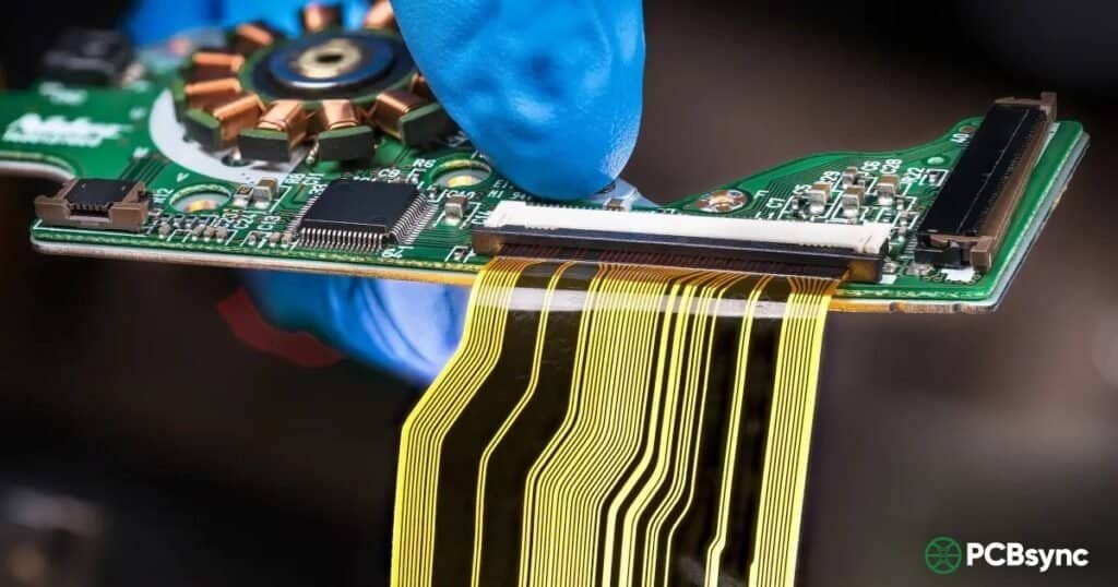
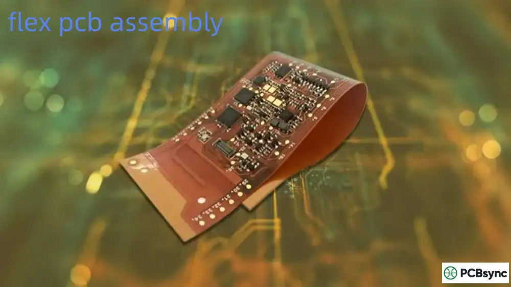
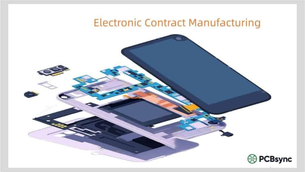
If you’ve ever torn down a smartphone, peeled back the layers of a smartwatch, or inspected the guts of a modern medical device, you’ve seen flex PCB assembly in action. These thin, bendable circuits have become the backbone of compact electronics, and for good reason—they go where rigid boards simply can’t.
I’ve spent over a decade working with flexible circuits, and I still find it fascinating how much engineering goes into making these things work reliably. Unlike traditional rigid PCBs, flex circuits demand a completely different mindset during design and assembly. Get it wrong, and you’re looking at cracked traces, delamination, or solder joints that fail after a few hundred bends.
This guide covers everything you need to know about flex PCB assembly—from material selection and bend radius calculations to the assembly process itself. Whether you’re an engineer designing your first flexible circuit or a procurement manager evaluating turnkey assembly partners, you’ll find practical, real-world insights here. No fluff, just the stuff that actually matters when you’re trying to get a reliable flex circuit into production.
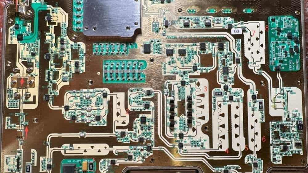
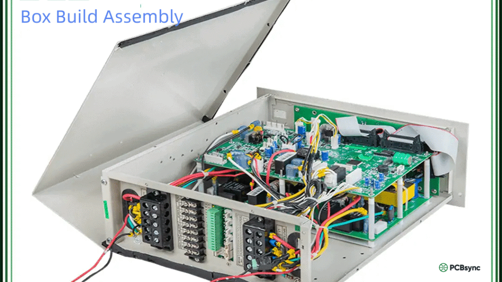
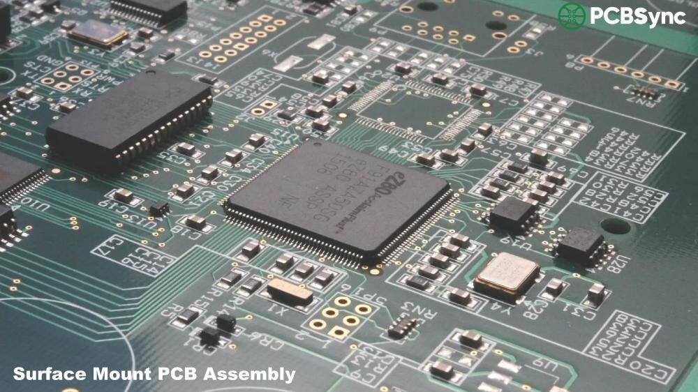
Flex PCB assembly is the process of mounting and soldering electronic components onto a flexible printed circuit board. Unlike rigid FR-4 boards that snap if you try to bend them, flex PCBs use thin, pliable substrates—typically polyimide (you might know it as Kapton)—that can twist, fold, and conform to three-dimensional shapes while maintaining electrical connectivity.
The assembly process shares similarities with rigid board assembly—you still have solder paste printing, pick-and-place, and reflow soldering—but the flexible substrate introduces complications that require specialized handling, fixturing, and process controls. You can’t just throw a flex circuit onto a standard SMT line and expect good results.
Here’s the critical distinction: flex circuits aren’t just “bendy rigid boards.” They’re engineered systems where mechanical and electrical requirements intersect. A successful flex PCB assembly considers not just component placement and routing, but also how the board will be handled during assembly, how it will flex in service, and what stresses it will endure over its lifetime.
Types of Flex PCBs You Should Know
Before diving into assembly specifics, let’s clarify the different flex circuit types, because the assembly approach varies significantly depending on what you’re working with.
Flex Type
Description
Best Applications
Single-Sided Flex
One conductive layer on flexible substrate. Simplest and most cost-effective option.
LED strips, simple connectors, cable replacements, keyboard membranes
Double-Sided Flex
Two conductive layers with plated through-holes (PTH) for interconnection.
Three or more conductive layers. Higher routing density but reduced flexibility.
Complex handheld devices, high-density interconnects, aerospace systems
Rigid-Flex
Combines rigid PCB sections with flexible interconnects in one integrated assembly.
Smartphones, laptops, medical implants, military/aerospace electronics
The type you choose directly impacts assembly complexity and cost. Single-sided flex circuits are straightforward to assemble, while rigid-flex requires careful consideration of how the assembly will be handled between rigid and flexible zones.
Key Applications of Flex PCB Assembly
Flex PCB assembly has penetrated nearly every industry where space, weight, or dynamic movement matters. Here’s where you’ll find these circuits doing the heavy lifting:
Consumer Electronics
Your smartphone contains multiple flex circuits—connecting the display to the main board, linking camera modules, and routing signals to antenna arrays. Laptops use rigid-flex designs to connect the screen to the keyboard assembly through that hinge you open and close thousands of times. Wearables like fitness trackers and smartwatches simply wouldn’t exist in their current form without flex PCB assembly.
Medical Devices
Medical applications demand the highest reliability standards. Flex circuits appear in hearing aids, pacemakers, insulin pumps, and diagnostic imaging equipment. The thin, lightweight nature of flex PCBs makes them ideal for implantable devices where patient comfort and device longevity are paramount. Assembly for medical flex circuits typically requires IPC Class 3 workmanship standards and extensive documentation.
Automotive Electronics
Modern vehicles are rolling computers, and flex circuits connect sensors, displays, and control units throughout the cabin and under the hood. Dashboard displays, steering wheel controls, and advanced driver-assistance systems (ADAS) all rely on flex PCB assembly. These applications must withstand temperature extremes, vibration, and decades of service life.
Aerospace and Defense
Weight savings matter when you’re launching something into orbit or keeping a fighter jet airborne. Flex circuits can reduce wiring harness weight by up to 75% compared to traditional round wire solutions. Military and aerospace applications often require rigid-flex designs that can handle extreme thermal cycling and mechanical stress while meeting strict reliability requirements per MIL-PRF-31032 and IPC-6013 Class 3/A.
Industrial and Robotics
Robotic arms, automated manufacturing equipment, and industrial sensors increasingly use flex circuits to route signals across moving joints. Dynamic flex applications—where the circuit bends repeatedly during operation—present unique design and assembly challenges that we’ll explore in detail.
After working on hundreds of flex circuit projects, I can tell you that most failures trace back to design decisions that didn’t account for the mechanical realities of flexible substrates. Here are the challenges that keep engineers up at night:
Bend Radius Calculations
The bend radius is the minimum radius at which you can safely bend a flex circuit without cracking the copper traces. Get this wrong, and you’re looking at premature failures. IPC-2223 provides the industry-standard guidelines, and here’s the simplified version:
Application Type
Layer Count
Min. Bend Radius
Static (bend-to-install)
1-2 layers
6× to 10× circuit thickness
Static (bend-to-install)
3-4 layers
15× to 25× circuit thickness
Dynamic (repeated flexing)
1-2 layers only
100× circuit thickness
Dynamic flex applications—where the circuit bends repeatedly during operation—are particularly demanding. I always recommend limiting dynamic flex zones to single or double-layer construction and using rolled annealed (RA) copper, which handles repeated bending far better than electrodeposited (ED) copper.
Component Placement Constraints
You can’t place components anywhere you want on a flex circuit. Components in or near bend zones will experience stress that can crack solder joints or cause pad lifting. The general rule: keep components at least 2.5mm (100 mils) away from any bend area. Heavy or tall components are especially problematic—they add mass that increases stress during bending.
When components must be placed near flex zones, consider adding stiffeners—rigid backing materials (typically FR-4 or polyimide) that reinforce the area around the component. Stiffeners add cost and thickness but dramatically improve reliability in challenging applications.
Trace Routing in Flex Zones
Routing traces through flex areas requires a different approach than rigid board design. Sharp corners concentrate stress and lead to cracking—always use curved traces with gradual bends. Traces should run perpendicular to the bend axis, and on multilayer flex, you should stagger traces on opposite layers rather than stacking them directly on top of each other.
Wide traces are more resistant to fatigue than narrow ones, but solid copper planes in flex zones are a disaster waiting to happen. If you need ground planes in flex areas, use a hatched or cross-hatched pattern to distribute stress more evenly.
Solder Joint Integrity
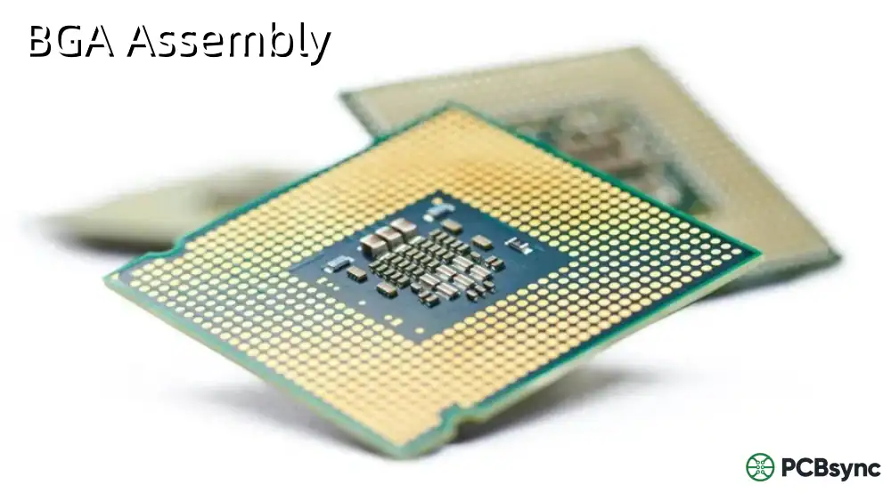
Solder joints on flex circuits face unique challenges. The flexible substrate means the board can move relative to components, stressing the solder connections. This is particularly problematic for fine-pitch components like BGAs or QFNs. Proper pad design with teardrop transitions, adequate annular rings, and consideration of solder paste volume all become critical factors in achieving reliable joints.
Signal Integrity Concerns
High-speed signals on flex circuits present additional challenges. The thin dielectric and changing geometry during flexing can affect impedance control. For applications requiring controlled impedance—typically 50Ω single-ended or 100Ω differential—you’ll need to work closely with your fabricator to achieve consistent results. Keep high-speed traces as short as possible through flex zones, and use proper grounding techniques to minimize EMI issues.
Solutions for Flex PCB Design Challenges
Now that we’ve covered what can go wrong, let’s talk about how to get it right. These are the practices I’ve seen work consistently across hundreds of successful flex PCB assembly projects:
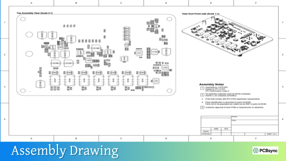
Design for Manufacturability (DFM) Review
Before committing to fabrication, get a thorough DFM review from your manufacturer. A good assembler will check pad sizes, trace routing, component spacing, and bend radius compliance. This step catches problems when they’re cheap to fix—on the computer—rather than expensive to fix—in production. At minimum, your DFM review should verify:
Component placement relative to bend zones
Trace routing through flex areas
Stiffener placement and adhesive zones
Via placement relative to bends (avoid vias in flex zones)
Coverlay openings and their alignment with pads
Material Selection Best Practices
Material choices make or break flex circuit reliability. For dynamic flex applications, always specify rolled annealed (RA) copper—it can withstand 100,000+ flex cycles compared to maybe 10,000 for electrodeposited (ED) copper. Polyimide remains the substrate of choice for most applications due to its excellent thermal stability and flexibility, though PET (polyester) can work for lower-temperature, cost-sensitive applications.
Adhesiveless (sometimes called “adhesiveless polyimide” or “2-layer flex”) constructions are thinner and more flexible than adhesive-based alternatives. If maximum flexibility matters, specify adhesiveless materials even though they cost more.
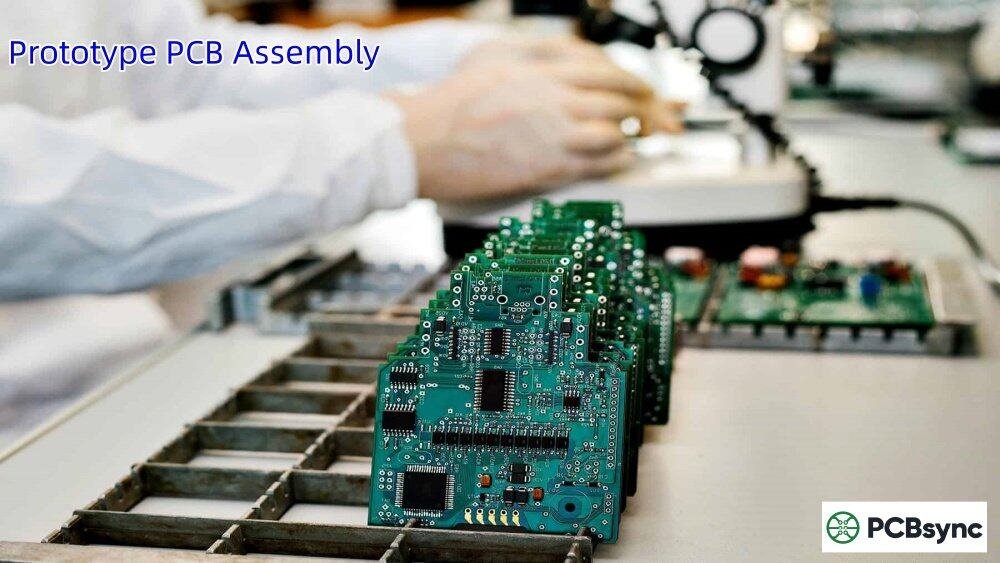
Prototype Testing Protocol
Never skip prototyping on a new flex design. Build prototype assemblies and test them under conditions that simulate—or exceed—the actual use environment. For dynamic flex, that means bend testing at the specified radius for more cycles than the design requirement. For static flex, verify that the assembly survives installation and any expected maintenance handling.
Environmental stress testing—temperature cycling, humidity exposure, vibration—often reveals weaknesses that aren’t apparent in initial testing. Plan for this testing in your development schedule, and budget accordingly.
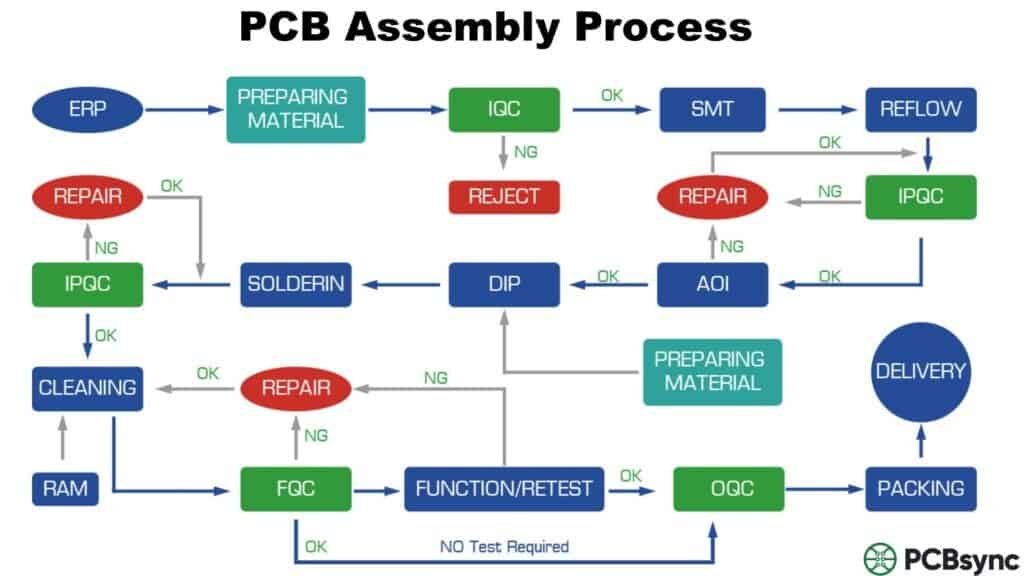
The Flex PCB Assembly Process Step-by-Step
The assembly process for flex circuits follows a similar flow to rigid board assembly, but every step requires additional care and often specialized equipment. Here’s what happens when your flex circuit hits the assembly line:
Step 1: Incoming Inspection and Baking
Flex circuits absorb moisture from the environment. If that moisture isn’t removed before reflow, it turns to steam and causes delamination or the dreaded “popcorning” effect. Standard practice is to bake flex circuits at 120°C for 4-6 hours before assembly. The exact time depends on material thickness and exposure history.
Step 2: Mounting to Carriers
You can’t run a floppy flex circuit through an SMT line without support. The circuit gets mounted to a rigid carrier—typically an FR-4 or aluminum pallet—using temporary adhesive or mechanical fixtures. The carrier must hold the flex flat and stable during paste printing and pick-and-place, then release cleanly after assembly without damaging the circuit.
Step 3: Solder Paste Printing
Stencil printing on flex circuits requires tighter process control than rigid boards. The compliant substrate can deflect under squeegee pressure, affecting paste volume consistency. Many assemblers use polyurethane squeegees instead of metal blades and rely on optical alignment systems to compensate for any registration drift in the flex material.
Step 4: Component Placement
Modern pick-and-place machines can handle flex circuits, but the vision systems may need calibration adjustments for the different optical properties of polyimide versus FR-4. Components should be placed gently—the flexible substrate is more susceptible to damage from aggressive nozzle contact than rigid boards.
Step 5: Reflow Soldering
Reflow profiles for flex circuits typically feature slower ramp rates and careful attention to cool-down rates. Rapid temperature changes can induce stress that warps the flex or damages solder joints. Convection reflow ovens with good temperature uniformity work best—infrared-heavy profiles can cause uneven heating on the thin substrate.
Step 6: Inspection and Testing
Post-assembly inspection includes automated optical inspection (AOI), X-ray for hidden joints (BGAs, QFNs), and electrical testing. Functional testing should include any bend or flex cycles the circuit will experience in its application. Many assemblers also perform in-circuit testing (ICT) or flying probe testing to verify connectivity.
Step 7: Stiffener Application and Final Assembly
If stiffeners weren’t pre-applied to the bare flex, they’re added after component assembly. Connectors that can’t survive reflow temperatures may be hand-soldered at this stage. Conformal coating or other protective treatments are applied if specified, and the assemblies receive final inspection before packaging.
Materials for Flex PCB Assembly
Understanding flex circuit materials helps you make informed decisions during design and vendor selection. Here’s a comparison of the key materials:
Material
Properties
Best For
Limitations
Polyimide (PI)
High temp resistance (-65°C to 150°C), excellent flex life, good chemical resistance
Lower cost, uniform thickness, adequate for static flex (~10K cycles)
Static flex, bend-to-install applications
Limited flex life, prone to cracking under repeated stress
Why Consider Turnkey Services for Flex PCB Assembly
Managing flex PCB assembly in-house requires specialized equipment, trained personnel, and process expertise that many companies don’t have—or don’t want to maintain. Turnkey assembly services handle everything from fabrication and component sourcing through final assembly and testing, giving you a single point of accountability for your flex circuit production.
When Turnkey Makes Sense
Prototype and Low Volume: Building flex circuit assembly capability for occasional projects rarely makes economic sense. Turnkey providers spread equipment and expertise costs across multiple customers.
Complex Rigid-Flex Designs: Rigid-flex assembly requires handling the board differently at various stages. Experienced turnkey providers have developed processes for these challenges.
Time-to-Market Pressure: A turnkey partner with materials in stock can cut weeks from your development schedule compared to sourcing boards and components separately.
Supply Chain Simplification: One vendor, one invoice, one contact point. Particularly valuable when dealing with component shortages or allocation issues.
What to Look for in a Turnkey Partner
Not all assembly houses handle flex circuits well. When evaluating turnkey providers for flex PCB assembly, verify:
Relevant certifications: ISO 9001 as baseline, ISO 13485 for medical, AS9100 for aerospace. IPC-A-610 Class 3 capability is essential for high-reliability work.
Flex-specific experience: Ask for examples of similar projects. A shop that mostly does rigid boards won’t have the same process maturity for flex.
DFM support: Good partners catch design issues before they become production problems. Ask about their review process.
Testing capabilities: Beyond AOI and ICT, can they perform environmental testing, bend testing, or application-specific functional tests?
Supply chain strength: A turnkey provider is only as good as their component sourcing. Ask about their distributor relationships and ability to handle allocation situations.
Useful Resources and Standards
Having the right reference materials makes all the difference in flex PCB design and assembly. Here are the resources I keep bookmarked:
Industry Standards
IPC-2223: Sectional Design Standard for Flexible Printed Boards – the definitive guide for flex circuit design requirements
IPC-6013: Qualification and Performance Specification for Flexible/Rigid-Flex Printed Boards
IPC-A-610: Acceptability of Electronic Assemblies – workmanship standards for assembly
MIL-PRF-31032: Performance specification for flex circuits in military applications
Material Specifications and Databases
DuPont Kapton Data Sheets: Technical specifications for polyimide films (dupont.com)
IPC-4204: Specification for Adhesive Coated Dielectric Films for Use as Cover Sheets
IPC-4203: Cover and Bonding Material Specifications for Flexible Printed Circuitry
Design Software with Flex Capabilities
Altium Designer: Integrated rigid-flex design with 3D bending visualization
Cadence Allegro: Enterprise-level flex and rigid-flex design tools
Mentor PADS/Xpedition: Comprehensive PCB design suite with flex support
KiCad: Open-source option with improving flex capabilities
Frequently Asked Questions About Flex PCB Assembly
What is the typical lead time for flex PCB assembly?
Lead times vary significantly based on complexity and volume. Simple single-sided flex circuits can be turned around in 1-2 weeks for prototypes. Complex multilayer rigid-flex assemblies typically require 3-6 weeks, including fabrication and assembly. If you need faster turns, expect to pay expedite premiums—sometimes 50-100% more than standard pricing. Always factor in component lead times, which can dominate the schedule for parts with long allocation cycles.
Can flex PCBs be reworked if components fail?
Yes, but carefully. Flex circuits are more delicate than rigid boards, and the thin substrate can be damaged by repeated heat cycles. Rework is possible for most SMT components using hot air or specialized tools, but you need operators experienced with flex materials. Large components or BGAs are particularly challenging—the heat required can cause coverlay separation or substrate distortion. For critical applications, it’s often more cost-effective to replace the assembly than risk rework damage.
How does flex PCB assembly cost compare to rigid board assembly?
Flex PCB assembly typically costs 2-4 times more than equivalent rigid board assembly. The premium comes from specialized materials (polyimide vs. FR-4), additional process steps (carrier mounting, pre-baking), lower assembly yields, and the engineering expertise required. Rigid-flex assemblies are even more expensive due to their complexity. However, flex circuits often eliminate connectors, reduce cable harness costs, and enable designs that wouldn’t be possible with rigid boards—so the total system cost may actually be lower.
What’s the maximum number of layers possible in a flex circuit?
While theoretically you can build flex circuits with many layers, practical limits exist. Most flex circuits use 1-4 layers, with 6 layers being common for complex applications. Beyond 6 layers, you’re typically looking at rigid-flex designs where the flex sections remain at lower layer counts (1-2 layers) while rigid sections handle the high-density routing. Every additional layer reduces flexibility and increases minimum bend radius, so the design requirement should drive the layer count—not the other way around.
Do I need special connectors for flex circuits?
Yes, in most cases. Standard through-hole connectors don’t work well on thin flex substrates. ZIF (Zero Insertion Force) connectors are the most common choice—they accept the flex circuit edge directly without soldering. FPC connectors come in various pitch sizes (0.3mm to 2.54mm) and configurations (top contact, bottom contact, dual contact). For higher current or more robust connections, some designs use board-to-board connectors mounted on stiffened sections of the flex, or direct soldering to a rigid PCB.
Quality Control in Flex PCB Assembly
Quality control for flex circuits requires inspection methods tailored to the unique failure modes of flexible substrates. Here’s what a robust quality program looks like:
Visual and Automated Optical Inspection
Every flex assembly should undergo 100% visual inspection for obvious defects—solder bridges, missing components, misaligned parts. Automated Optical Inspection (AOI) catches defects that human inspectors might miss, particularly on fine-pitch components. However, AOI systems need proper programming for flex circuits, as the different optical properties of polyimide can confuse systems calibrated for FR-4.
X-Ray Inspection for Hidden Joints
BGAs, QFNs, and other bottom-terminated components hide their solder joints from optical inspection. X-ray inspection reveals voids, bridging, and insufficient solder volume in these hidden connections. For high-reliability applications, 100% X-ray inspection of hidden joints is standard practice.
Electrical Testing
In-Circuit Testing (ICT) or flying probe testing verifies electrical connectivity and component values. For flex circuits, test fixtures must support the board without stressing flex zones. Flying probe testing offers more flexibility for low-volume production and doesn’t require expensive custom fixtures.
Mechanical and Environmental Testing
Application-specific testing validates that the assembled flex circuit will survive its intended use environment. Bend testing—cycling the circuit through its specified bend radius thousands of times—reveals weaknesses in trace routing and solder joint design. Temperature cycling, humidity exposure, and vibration testing simulate years of field exposure in accelerated timeframes.
Wrapping Up
Flex PCB assembly sits at the intersection of electrical engineering and mechanical design. Getting it right requires understanding both domains and respecting the unique properties of flexible substrates. The challenges are real—bend radius limitations, component placement constraints, material selection decisions—but so are the rewards: lighter, more compact, more reliable electronic products that simply couldn’t exist with rigid boards alone.
Whether you’re designing your first flex circuit or your fiftieth, the fundamentals remain the same: understand your application requirements, design with manufacturing in mind, prototype before committing to production, and partner with assemblers who have real flex circuit expertise. Do those things, and you’ll join the ranks of engineers building the flexible electronics that power everything from pacemakers to spacecraft.
If there’s one takeaway from this guide, it’s this: flex PCB assembly isn’t just “different”—it’s a specialized discipline that rewards careful planning and punishes shortcuts. Invest the time upfront to get your design right, choose your materials and manufacturing partners wisely, and you’ll be rewarded with flex circuits that perform reliably for years of service.
Inquire: Call 0086-755-23203480, or reach out via the form below/your sales contact to discuss our design, manufacturing, and assembly capabilities.
Quote: Email your PCB files to Sales@pcbsync.com (Preferred for large files) or submit online. We will contact you promptly. Please ensure your email is correct.
Notes: For PCB fabrication, we require PCB design file in Gerber RS-274X format (most preferred), *.PCB/DDB (Protel, inform your program version) format or *.BRD (Eagle) format. For PCB assembly, we require PCB design file in above mentioned format, drilling file and BOM. Click to download BOM template To avoid file missing, please include all files into one folder and compress it into .zip or .rar format.


