Inquire: Call 0086-755-23203480, or reach out via the form below/your sales contact to discuss our design, manufacturing, and assembly capabilities.
Quote: Email your PCB files to Sales@pcbsync.com (Preferred for large files) or submit online. We will contact you promptly. Please ensure your email is correct.
Notes: For PCB fabrication, we require PCB design file in Gerber RS-274X format (most preferred), *.PCB/DDB (Protel, inform your program version) format or *.BRD (Eagle) format. For PCB assembly, we require PCB design file in above mentioned format, drilling file and BOM. Click to download BOM template To avoid file missing, please include all files into one folder and compress it into .zip or .rar format.
EPM240 & MAX II CPLD: Complete Guide to Altera’s Popular CPLDs
If you’re looking for an affordable, reliable entry point into the world of programmable logic devices, the Altera EPM240 and MAX II CPLD family should be at the top of your list. After working with dozens of different PLDs over my engineering career, I keep coming back to these devices for glue logic, interface bridging, and countless other applications where instant-on operation and predictable timing are essential. This comprehensive guide will walk you through everything you need to know about the EPM240T100C5N, its variants, and the broader MAX II and MAX V CPLD families.
The CPLD EPM240 has become something of a legend in the embedded systems community. Originally released by Altera (now Intel) as part of the MAX II family, it struck the perfect balance between capability and simplicity that made it accessible to hobbyists while remaining capable enough for professional applications. The EPM240T100C5N variant in particular has become ubiquitous on low-cost development boards available from Chinese manufacturers, making it the go-to choice for engineers and students learning programmable logic design.
Whether you’re designing a power sequencing controller, implementing protocol conversion logic, or simply need some fast glue logic between components, understanding the capabilities and limitations of Altera MAX2 CPLDs will help you make informed design decisions. This guide covers not just the EPM240 but also the newer MAX V family including popular devices like the 5M240ZT100C5N, 5M80ZE64C5N, and 5M160Z variants that offer improved power efficiency and additional features.
Understanding CPLDs: What Makes the MAX II Family Special
A Complex Programmable Logic Device (CPLD) is a type of programmable integrated circuit that allows engineers to implement custom digital logic functions. Unlike microcontrollers that execute software instructions sequentially, CPLDs implement logic directly in hardware, providing deterministic timing and instant-on operation. The MAX2 CPLD family from Altera revolutionized this space by combining traditional CPLD benefits with flash-based configuration storage and FPGA-like architecture.
CPLD vs FPGA: When to Choose Each Technology
The question of whether to use a CPLD or FPGA comes up constantly in design discussions. CPLDs like the Altera EPM240 excel in applications requiring instant power-on operation (no boot time), predictable pin-to-pin timing, lower power consumption, and simpler designs with moderate logic requirements. FPGAs, on the other hand, offer vastly more logic capacity, embedded memory blocks, DSP resources, and high-speed transceivers for complex applications like video processing, networking, and high-performance computing.
The MAX II architecture is technically based on FPGA-style look-up tables (LUTs) rather than traditional CPLD product terms, but the integrated flash configuration memory provides instant-on operation that traditional FPGAs lack. This hybrid approach gives you FPGA-like flexibility with CPLD-like simplicity. When your design needs 240 to 2,210 logic elements, non-volatile configuration, and you don’t need the advanced features of modern FPGAs, the MAX II and MAXV CPLD families offer an excellent cost-performance tradeoff.
Altera EPM240: The Most Popular CPLD for Learning and Prototyping
The EPM240 is the smallest member of the MAX II CPLD family, featuring 240 logic elements (LEs), 80 user I/O pins (in the TQFP-100 package), 8 Kbits of user flash memory (UFM), and operation at up to 304 MHz. Despite being the “entry-level” device, the EPM240 provides enough resources for a surprisingly wide range of applications. I’ve personally used it for everything from simple LED controllers to complete UART protocol converters and SPI-to-parallel interfaces.
EPM240T100C5N Technical Specifications
The EPM240T100C5N is the most commonly used variant, packaged in a 100-pin TQFP (Thin Quad Flat Pack) with commercial temperature rating (0°C to 85°C) and speed grade 5. The ‘T100’ indicates the TQFP-100 package, ‘C’ indicates commercial temperature range, ‘5’ indicates the fastest speed grade, and ‘N’ indicates lead-free packaging. Understanding this nomenclature helps when selecting alternative variants for your specific requirements.
Parameter
EPM240T100C5N Specification
Logic Elements (LEs)
240
Equivalent Macrocells
192 typical (128-240 range)
Maximum User I/O Pins
80 (TQFP-100 package)
User Flash Memory (UFM)
8,192 bits (8 Kbits)
Global Clocks
4 (GCLK[3:0])
Pin-to-Pin Delay (tPD)
4.7 ns typical
Maximum Counter Frequency
304 MHz
Core Voltage (VCCINT)
2.5V or 3.3V (internal 1.8V regulator)
I/O Voltage (VCCIO)
1.5V, 1.8V, 2.5V, or 3.3V
I/O Banks
2 (independent VCCIO per bank)
Process Technology
0.18µm, 6-layer metal flash
Package Options
TQFP-100, MBGA-68, FBGA-256
EPM240 Variant Part Numbers Explained
The Altera EPM240T100C5N is just one of several EPM240 variants. Understanding the part numbering helps you select the right device for your application. The EPM240M100I5N, for example, uses the ‘M’ prefix indicating an MBGA (Micro Ball Grid Array) package and ‘I’ for industrial temperature range (-40°C to 100°C). The CPLD EPM240T100C5 (without the ‘N’ suffix) refers to the leaded version, while all current production uses lead-free ‘N’ suffix parts. Speed grades range from 3 (slowest, lowest power) to 5 (fastest), with speed grade 4 offering a middle-ground option.
Complete MAX II CPLD Family Overview
The MAX II family extends beyond the EPM240 to include devices with up to 2,210 logic elements for more demanding applications. All MAX II devices share the same architecture, toolchain, and programming methodology, making it easy to migrate designs between density options as requirements evolve. The family includes standard MAX II devices, the ultra-low-power MAX IIG variants (1.8V core), and the MAX IIZ series optimized for battery-powered applications.
Device
LEs
Macrocells
Max I/O
tPD (ns)
fCNT (MHz)
EPM240
240
192
80
4.7
304
EPM570
570
440
160
5.4
304
EPM1270
1,270
980
212
6.2
304
EPM2210
2,210
1,700
272
7.0
304
MAX V CPLD Family: The Next Generation
The MAXV CPLD family represents Altera’s evolution of the MAX II architecture, offering improved power efficiency, an internal oscillator, and additional features while maintaining backward compatibility with MAX II designs. The MAX V family includes devices from the tiny 5M40ZE64C5N with 40 LEs to the 5M2210ZF256C5N with 2,210 LEs. Popular mid-range devices like the 5M80ZE64C5N, 5M160Z, and 5M240ZT100C5N provide excellent options for designs that have outgrown the EPM240 but don’t require a full FPGA.
Key MAX V Improvements Over MAX II
Internal Oscillator: Built-in oscillator eliminates need for external crystal in many applications
Lower Core Voltage: 1.8V VCCINT (vs 2.5/3.3V for MAX II) reduces power consumption by up to 50%
Fast Power-On Reset: Integrated POR circuit simplifies system design
Programmable Drive Strength: Adjustable output current for signal integrity optimization
Hot-Socketing: Full hot-socketing support for field-replaceable designs
Lower Static Power: As low as 45µW static power for battery-powered applications
Popular MAX V Device Options
Device
LEs
Macrocells
Max I/O
tPD (ns)
fCNT (MHz)
5M40Z
40
32
54
7.5
152
5M80Z
80
64
79
7.5
152
5M160Z
160
128
79
7.5
152
5M240Z
240
192
114
7.5
152
5M570Z
570
440
159
9.0
152
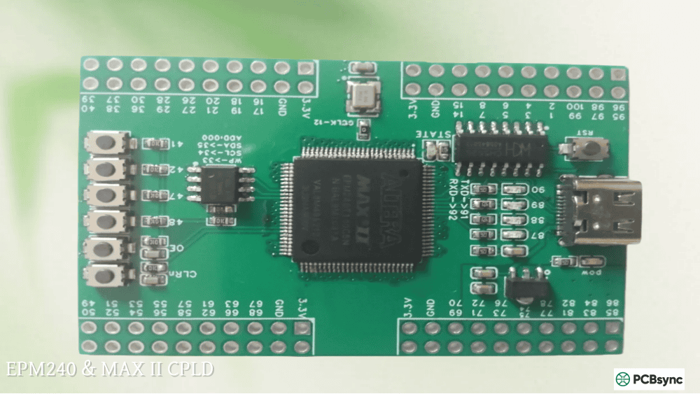
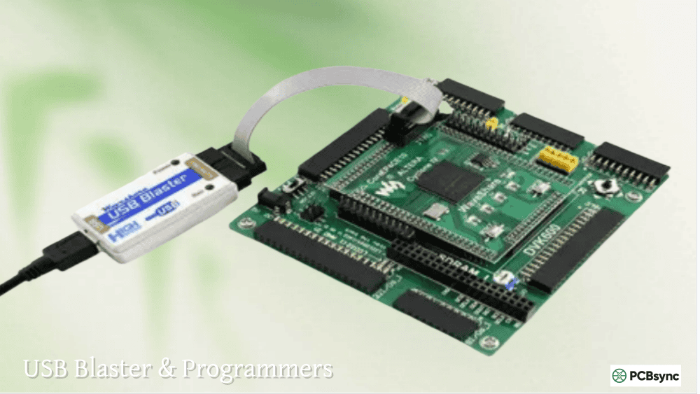
EPM240 Development Boards and Programming Setup
One of the reasons the CPLD EPM240 became so popular is the availability of extremely affordable development boards. You can find EPM240T100C5N development boards on AliExpress, eBay, and Amazon for around $8-15 including a USB Blaster programmer clone. These boards typically include the CPLD, a JTAG header, onboard 3.3V regulator, 50MHz crystal oscillator, one or more programmable LEDs, and pin headers exposing all I/O pins for easy prototyping.
Typical EPM240 Development Board Features
EPM240T100C5N CPLD in TQFP-100 package
10-pin JTAG header for programming and debugging
50MHz onboard active crystal oscillator
Onboard 3.3V LDO voltage regulator
5V DC power jack with power switch
One or more user-programmable LEDs
All I/O pins accessible via 2.54mm pin headers
Board dimensions typically 50mm x 70mm
Setting Up Quartus Prime for CPLD Development
Intel’s Quartus Prime Lite Edition is the free development tool for programming MAX II and MAX V CPLDs. The software includes schematic capture, Verilog/VHDL synthesis, simulation, and the programmer utility. For MAX II devices, you’ll need to download the legacy device support package separately since these older devices aren’t included in the default Quartus Prime installation.
Download Quartus Prime Lite Edition from Intel’s FPGA Software Download Center
Download and install the “MAX II, MAX V device support” package separately
Connect your USB Blaster programmer to your PC
Install USB Blaster drivers from <Quartus>/drivers/usb-blaster directory
Create a new project and select EPM240T100C5 (or your specific device)
Write your design in Verilog, VHDL, or schematic entry
Compile the project and assign pins using Pin Planner
Use the Programmer tool to download the .pof file to the CPLD
Important Tip: Under Device & Pin Options, set “Reserve all unused pins” to “As input tri-stated” rather than the default “As output driving ground.” This prevents mysterious behavior when debugging and makes probing easier during development.
Common Applications for MAX II and MAX V CPLDs
The versatility of the Altera EPM240 and its larger siblings makes them suitable for a wide range of applications. Their instant-on operation, non-volatile configuration, and predictable timing characteristics make CPLDs the preferred choice over FPGAs and microcontrollers for many specific use cases.
Glue Logic and Interface Bridging
Perhaps the most common use for CPLDs is implementing “glue logic” – the miscellaneous logic functions needed to connect various components in a system. This might include bus width conversion (8-bit to 16-bit), voltage level shifting logic, address decoding, chip select generation, and simple state machines. The EPM240’s 80 I/O pins and 240 logic elements can easily handle the glue logic requirements that would otherwise require multiple discrete logic ICs, saving board space and improving reliability.
Power Sequencing and Management
Complex systems often require specific power-up and power-down sequences to prevent damage to components or ensure proper initialization. CPLDs excel at implementing power sequencing controllers because they power on instantly and begin executing logic immediately. You can implement complex multi-rail sequencing with programmable delays, fault detection, and proper shutdown sequences – all in a single device that’s ready to go the moment power is applied.
Protocol Conversion and I/O Expansion
Converting between communication protocols is another excellent application for MAX II CPLDs. Common examples include SPI to parallel conversion, UART protocol handling, I2C expansion, PWM generation, and encoder interfaces. The User Flash Memory (UFM) in MAX II devices can store configuration data, lookup tables, or calibration values that persist across power cycles without external EEPROM.
FPGA Configuration Management
In systems using SRAM-based FPGAs, a CPLD often handles the configuration loading process. The CPLD boots instantly at power-up and manages the FPGA configuration sequence, including reading configuration data from external flash memory and streaming it to the FPGA. This architecture allows for features like multi-boot configurations, golden image fallback, and remote update capability.
Essential Resources for MAX II and MAX V Development
Official Intel Documentation
MAX II Device Handbook: Comprehensive technical documentation covering architecture, pinouts, and specifications
MAX V Device Handbook: Complete reference for MAX V family devices
AN-428 MAX II Design Guidelines: Best practices for PCB layout and device usage
Quartus Prime User Guide: Software tutorials and reference documentation
Software Downloads
Quartus Prime Lite Edition: https://www.intel.com/content/www/us/en/software-kit/download/intel-quartus-prime-lite-edition-design-software.html
MAX II/MAX V Device Support: Download separately from Quartus download page
USB Blaster Drivers: Included with Quartus installation in /drivers/usb-blaster
Where to Buy EPM240 Development Boards
AliExpress: Search “EPM240 CPLD development board” – typically $8-15 with USB Blaster
Amazon: Higher prices but faster shipping and returns
eBay: Good selection of boards and programmers
DigiKey/Mouser: For individual EPM240T100C5N chips and professional development kits
Frequently Asked Questions About EPM240 and MAX II CPLDs
What version of Quartus should I use for EPM240 programming?
Intel recommends Quartus Prime Lite Edition for MAX II and MAX V CPLD development. You’ll need to download the device support package separately since MAX II isn’t included by default. Quartus 13.0 SP1 and 13.1 are popular choices that still support MAX II natively without additional downloads. For the latest Quartus versions, ensure you install the legacy device support after the main installation. Note that newer Quartus versions may require more disk space and have heavier system requirements, so some developers prefer sticking with Quartus 13.x for CPLD-only work.
Can I program the EPM240 without a USB Blaster?
The official method uses JTAG programming via USB Blaster or compatible programmer. While there are alternative methods using tools like OpenOCD with cheap FT232-based adapters, these approaches require more setup and troubleshooting. The USB Blaster clones available for under $5 work reliably and are recommended for beginners. For production programming, Intel offers standalone programming hardware and third-party gang programmers support MAX II devices. Some engineers have also had success using Raspberry Pi GPIO pins with appropriate level shifting to program CPLDs via JTAG, though this requires careful attention to signal integrity and timing.
How does the EPM240 compare to Arduino for simple logic tasks?
The EPM240 and Arduino serve fundamentally different purposes. Arduino excels at sequential programming tasks and analog input but introduces latency due to software execution. The EPM240 implements logic directly in hardware, providing nanosecond response times and true parallel execution. For tasks requiring precise timing (like interfacing with legacy parallel buses or generating specific waveforms), the CPLD is far superior. For tasks requiring complex calculations, floating-point math, or analog sensing, the Arduino is easier to use. Many projects benefit from combining both: using a microcontroller for high-level control and a CPLD for time-critical interface logic. The EPM240 can handle dozens of simultaneous I/O operations in parallel, while an Arduino must process them sequentially.
Should I choose MAX II (EPM240) or MAX V (5M240Z) for a new design?
For new designs, the MAX V family (like the 5M240ZT100C5N) is generally preferred due to its lower power consumption, built-in oscillator, and continued availability. The MAX V uses 1.8V core voltage versus 2.5/3.3V for MAX II, resulting in significantly lower power consumption – critical for battery-powered applications. However, if you’re learning on existing EPM240 development boards or maintaining legacy designs, the MAX II devices remain fully supported and are excellent choices. Both families use the same Quartus toolchain and designs can be easily migrated between them with minor pin assignment changes. The MAX V’s internal oscillator is particularly useful for eliminating external crystal components in cost-sensitive designs.
What’s the difference between .pof and .sof files in Quartus?
POF (Programmer Object File) is for non-volatile programming – the configuration is stored in the CPLD’s internal flash and persists across power cycles. SOF (SRAM Object File) is primarily used with FPGAs for volatile configuration that needs to be reloaded at each power-up. For MAX II and MAX V CPLDs, you’ll typically use .pof files since these devices have built-in flash memory. The Quartus compiler generates both file types, but the Programmer tool uses the .pof for CPLD devices. You can also convert to other formats like .svf (Serial Vector Format) for use with third-party programmers and automated test equipment.
Troubleshooting Common EPM240 and MAX II CPLD Issues
Even experienced engineers occasionally encounter issues when working with CPLDs. Here are solutions to the most common problems you’ll face when developing with the Altera EPM240 and MAX II family, based on years of practical experience debugging these devices.
USB Blaster Not Detected in Quartus Programmer
This is the most frequently encountered issue, especially on Windows systems. First, verify the USB Blaster appears in Device Manager – it may show as an unrecognized device requiring driver installation. Navigate to your Quartus installation directory and locate the drivers/usb-blaster folder. Right-click the device in Device Manager, select Update Driver, and browse to this folder. If using Linux, create appropriate udev rules to grant non-root access to the USB device. Sometimes simply power cycling the development board and reconnecting the USB Blaster resolves intermittent detection issues. Cheap USB Blaster clones occasionally have quality issues – if problems persist, try a different clone or invest in a genuine programmer.
JTAG Chain Broken or Device Not Found Errors
When the Programmer reports JTAG chain errors, start by verifying the development board is properly powered. The USB Blaster typically doesn’t supply power to the target board, so you need external power via the DC jack or appropriate pins. Check that the JTAG ribbon cable is properly seated on both ends and oriented correctly – pin 1 markings should align. If using long JTAG cables or operating in electrically noisy environments, try reducing the JTAG clock frequency in Quartus Programmer settings. The CPLD’s JTAG pins (TDI, TDO, TMS, TCK) should not be connected to anything else on your board that might interfere with programming signals.
Design Works in Simulation but Not on Hardware
When designs simulate correctly but fail on actual hardware, pin assignments are the first thing to check. Use the Pin Planner tool to verify your signal assignments match the actual board connections. Pay particular attention to clock pins – the EPM240 has dedicated global clock inputs (GCLK0-3) that provide the best timing characteristics. Using a regular I/O pin for clock input can cause timing problems. Also check that unused pins are configured as “input tri-stated” rather than driving ground, which can cause unexpected behavior if pins are accidentally connected to something on your board.
Design Too Large for Selected Device
If Quartus reports your design exceeds available resources, you have several options. First, review your HDL code for inefficiencies – deeply nested if/else statements, unnecessary registers, and poorly optimized state machines can waste logic elements. Enable resource-saving compiler options in Quartus. Consider using the device’s User Flash Memory (UFM) for lookup tables instead of implementing them in logic. If the design genuinely requires more resources, migrate to a larger device like the EPM570 or EPM1270 which offer 570 and 1,270 logic elements respectively while maintaining pin compatibility in many packages.
Design Best Practices for MAX II and MAX V CPLDs
Following established best practices when designing for CPLDs will save you debugging time and produce more reliable results. These guidelines apply to both MAX II devices like the EPM240 and the newer MAX V family.
PCB Layout Considerations for EPM240
Proper PCB layout is essential for reliable CPLD operation. Place decoupling capacitors (0.1µF ceramic) as close as possible to each VCCINT and VCCIO power pin – the EPM240T100C5N has multiple power pins that all require bypassing. Use a solid ground plane and avoid routing signals under the CPLD package where possible. Keep JTAG traces short and away from high-speed signals to prevent programming issues. For the 50MHz clock input common on development boards, use controlled impedance traces if the crystal oscillator is more than a few centimeters from the CPLD.
HDL Coding Style for Efficient Resource Usage
Writing efficient Verilog or VHDL code for CPLDs requires different considerations than FPGA development. Avoid inferred latches by ensuring all paths through combinational logic are fully defined – use default assignments at the beginning of always blocks. Register your outputs when possible to improve timing and reduce glitches. Use the global clock networks (GCLK pins) for all clocked logic to ensure proper timing. Avoid asynchronous resets when possible, or use the device’s global clear network. Keep state machines simple and well-encoded – one-hot encoding often produces faster results in CPLDs than binary encoding.
Use synchronous design: All flip-flops should be clocked from global clock networks
Avoid combinational loops: These create unpredictable behavior and timing issues
Register I/O signals: Input and output registers improve timing margins
Use constraints: Define timing constraints to help the compiler optimize your design
Conclusion: Getting Started with EPM240 and MAX II CPLDs
The Altera EPM240 and the broader MAX II CPLD family represent an excellent entry point into programmable logic design. With development boards available for under $15 and free software tools from Intel, there’s never been a more accessible time to learn CPLD development. The skills you develop working with MAX II devices transfer directly to larger CPLDs and FPGAs, making this an investment in your engineering capabilities that will pay dividends throughout your career. The EPM240T100C5N in particular has become the de facto standard for learning programmable logic because of its widespread availability and extensive community support.
For professional applications, the EPM240T100C5N and its family members continue to offer compelling advantages: instant-on operation without boot delay, predictable pin-to-pin timing for time-critical interfaces, non-volatile configuration that survives power cycles, and robust reliability proven across millions of deployed systems in demanding industrial environments. Whether you’re implementing power sequencing, protocol conversion, custom interface logic, or FPGA configuration management, MAX II and MAXV CPLDs provide a mature, well-documented solution that has stood the test of time across countless production deployments worldwide.
Start with a simple LED blink project to verify your toolchain and programming setup, progress to implementing basic logic functions like counters and shift registers, and you’ll quickly discover the unique satisfaction of designing digital hardware directly in silicon. The CPLD EPM240 development board on your bench today could be the beginning of a journey into the fascinating world of programmable logic design that opens doors to FPGA development, digital system architecture, and hardware engineering roles that are increasingly in demand in today’s technology-driven world.
Inquire: Call 0086-755-23203480, or reach out via the form below/your sales contact to discuss our design, manufacturing, and assembly capabilities.
Quote: Email your PCB files to Sales@pcbsync.com (Preferred for large files) or submit online. We will contact you promptly. Please ensure your email is correct.
Notes: For PCB fabrication, we require PCB design file in Gerber RS-274X format (most preferred), *.PCB/DDB (Protel, inform your program version) format or *.BRD (Eagle) format. For PCB assembly, we require PCB design file in above mentioned format, drilling file and BOM. Click to download BOM template To avoid file missing, please include all files into one folder and compress it into .zip or .rar format.


