Inquire: Call 0086-755-23203480, or reach out via the form below/your sales contact to discuss our design, manufacturing, and assembly capabilities.
Quote: Email your PCB files to Sales@pcbsync.com (Preferred for large files) or submit online. We will contact you promptly. Please ensure your email is correct.
Notes: For PCB fabrication, we require PCB design file in Gerber RS-274X format (most preferred), *.PCB/DDB (Protel, inform your program version) format or *.BRD (Eagle) format. For PCB assembly, we require PCB design file in above mentioned format, drilling file and BOM. Click to download BOM template To avoid file missing, please include all files into one folder and compress it into .zip or .rar format.
If you’ve ever had a PCB fail in the field weeks after it passed all your bench tests, you know how frustrating—and expensive—latent defects can be. That’s exactly why Environmental Stress Screening exists. After spending over a decade working with electronic assemblies in aerospace and industrial applications, I’ve seen firsthand how a well-designed ESS program separates reliable products from warranty nightmares.
Environmental Stress Screening is not a test in the traditional sense. There’s no pass/fail criteria. Instead, it’s a manufacturing process designed to force hidden defects to reveal themselves before your product ever reaches the customer. In this guide, I’ll walk you through everything you need to know about ESS—from the fundamentals to implementation strategies that actually work on the production floor.
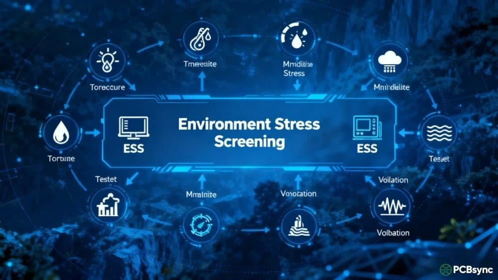
Environmental Stress Screening (ESS) is a process of exposing newly manufactured electronic products to controlled environmental stresses—primarily temperature cycling and vibration—to precipitate latent defects that would otherwise escape traditional inspection and testing. The key word here is “precipitate.” We’re not trying to break good products; we’re trying to accelerate the failure of weak ones.
The concept is straightforward: every manufacturing process introduces some level of defects. Visual inspection catches obvious problems. Functional testing catches electrical failures. But neither can reliably detect latent defects—those subtle flaws like marginal solder joints, contaminated components, or improperly seated connectors that work fine on the bench but fail after a few weeks or months in the field.
ESS subjects 100% of manufactured units to environmental stresses that accelerate these latent defects to failure while the product is still in the factory. The surviving population has measurably higher reliability than an unscreened population.
The Bathtub Curve and Infant Mortality
To understand why ESS works, you need to understand the bathtub curve—the classic reliability model that describes failure rates over a product’s lifetime:
The infant mortality phase is your enemy. According to the Telcordia reliability prediction standard (SR-332), the failure rate of an unscreened population can be four times higher at initial deployment than it will be after one year. ESS essentially compresses that infant mortality period into hours instead of months, catching those failures before shipment.
Types of Environmental Stresses Used in ESS
Not all stresses are created equal when it comes to precipitating defects. Based on extensive studies by the Institute of Environmental Sciences and Technology (IEST) and military research, two types of stress dominate effective ESS programs.
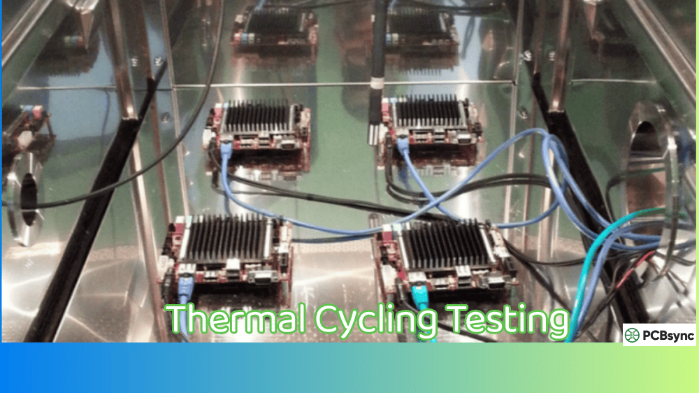
Temperature Cycling
Temperature cycling is consistently rated as the most effective stress for detecting latent defects in electronic assemblies. Research shows that temperature cycling detects approximately two-thirds more defects than vibration alone.
Here’s why it works so well: when you cycle an assembly through temperature extremes, differential thermal expansion creates mechanical stress on solder joints, component leads, and PCB substrates. A marginal solder joint that passes room-temperature testing will crack when subjected to repeated thermal expansion and contraction.
Recommended Temperature Cycling Parameters:
Parameter
Baseline Value
Notes
Temperature Range
-40°C to +75°C
Wider is better, within component limits
Rate of Change
5°C to 15°C per minute
Higher rates are more effective
Number of Cycles
20-30 cycles
Monitor failure rates to optimize
Dwell Time
10-15 minutes at extremes
Product must reach temperature
Air Velocity
Minimum 750 ft/min
Critical for uniform stress application
The temperature extremes should be set as far apart as possible while staying within the operating limits of your components. I’ve seen engineers make the mistake of being too conservative—using a 40°C range when their components can handle 100°C. You’re leaving defects on the table.
Random Vibration
Random vibration is the second most effective stress type for ESS. Unlike sinusoidal vibration, random vibration excites all resonant frequencies simultaneously, which is more representative of real-world conditions and more effective at precipitating defects.
The standard reference is the NAVMAT P-9492 profile, which specifies:
Frequency Range
Vibration Level
20-80 Hz
0.01 G²/Hz increasing at 3 dB/octave
80-350 Hz
0.04 G²/Hz flat
350-2000 Hz
Decreasing at -3 dB/octave
Random vibration is particularly effective at finding:
Loose hardware and fasteners
Poorly seated connectors
Wire harness problems
Cracked ceramic components
Marginal BGA and QFP solder joints
Combined Environment Testing
Studies consistently show that applying temperature cycling and vibration simultaneously is more effective than sequential application. The combined stresses create synergistic effects that precipitate defects neither stress would catch alone.
For production screening, a typical combined environment profile applies random vibration during the temperature transition ramps, then reduces or eliminates vibration during the dwell periods at temperature extremes. This approach maximizes defect precipitation while minimizing screening time.
Defects Detected by Environmental Stress Screening
One question I get frequently is: “What exactly will ESS catch that my other testing misses?” Here’s a breakdown of the most common defect types that ESS precipitates:
Solder Joint Defects
Defect Type
Description
ESS Detection Method
Cold Solder Joint
Rough, grainy joint from insufficient heat
Temperature cycling causes crack propagation
Solder Bridge
Unintended connection between adjacent pads
Thermal expansion reveals intermittent shorts
Insufficient Solder
Underfilled joint with weak mechanical bond
Vibration and thermal stress cause opens
Cracked Solder
Stress fractures in solder material
Temperature cycling accelerates crack growth
Head-in-Pillow (BGA)
BGA ball contacts but doesn’t properly wet
Combined stress reveals intermittent connection
Component Defects
Defect Type
Description
ESS Detection Method
Marginal Capacitors
Out-of-spec or weak dielectric
Temperature and voltage cycling cause breakdown
Contaminated ICs
Moisture or particle contamination
Humidity and temperature reveal leakage
Cracked Ceramics
Micro-cracks in ceramic packages
Thermal shock propagates cracks
Weak Wire Bonds
Poor internal chip connections
Temperature cycling and vibration cause opens
Workmanship Defects
Defect Type
Description
ESS Detection Method
Loose Connectors
Improperly seated or partially engaged
Vibration reveals intermittent connections
Missing Hardware
Screws, washers, or fasteners not installed
Vibration causes mechanical failures
Damaged PCB Traces
Scratches or cracks in copper traces
Thermal stress opens damaged traces
Lifted Pads
Pad separation from PCB substrate
Temperature cycling completes separation
ESS vs. HALT vs. HASS: Understanding the Differences
These three acronyms get confused constantly, so let me clarify:
Characteristic
ESS
HALT
HASS
Full Name
Environmental Stress Screening
Highly Accelerated Life Testing
Highly Accelerated Stress Screening
When Used
Production (100% of units)
Design/development phase
Production (100% of units)
Stress Levels
Within specification limits
Beyond spec to destruction
Beyond spec, below destruct limits
Purpose
Detect manufacturing defects
Find design weaknesses
Detect manufacturing defects quickly
Duration
Hours to days
Days (until failure)
Minutes to hours
Destructive?
No (for good units)
Yes (intentionally)
No (for good units)
HALT is a design validation tool. You push prototypes until they break to find the fundamental limits of your design. The goal is discovering failure modes, not screening production units.
ESS is the traditional production screening approach. Stress levels stay within the product’s specified operating limits. It’s effective but can require many hours or even days to complete.
HASS uses the information from HALT to create an aggressive but safe production screen. Because you know the actual operating limits (from HALT), you can apply higher stresses—typically 80-85% of the operating limit—which precipitates defects much faster than traditional ESS. A HASS screen that takes 1-2 hours might be equivalent to an ESS screen taking 8-24 hours.
If you’ve done HALT during product development, HASS is usually the better choice for production. If you haven’t characterized your operating limits, start with ESS using conservative parameters.
Implementing an ESS Program: Practical Considerations
Getting ESS right requires more than buying a thermal chamber and running product through it. Here’s what I’ve learned implementing ESS programs across multiple manufacturing facilities.
Choosing Your Screening Level
ESS can be performed at various assembly levels, each with trade-offs:
Assembly Level
Advantages
Disadvantages
Component
Catches defects at source
Expensive, component-level chambers needed
PCB Assembly
Most common, cost-effective balance
May not stress system-level interfaces
Subassembly
Tests interfaces between boards
More complex fixturing
System
Tests complete product
Expensive, long screen times
For most commercial electronics, PCB assembly level screening provides the best return on investment. You catch the majority of defects at a relatively early stage where rework is still feasible.
Equipment Requirements
An ESS system typically consists of:
Environmental Chamber: Must support rapid temperature transitions (5-15°C/min minimum) with high air velocity (750+ ft/min)
Vibration System: Electrodynamic or repetitive shock shakers for random vibration
Fixturing: Custom fixtures to mount units and route test connections
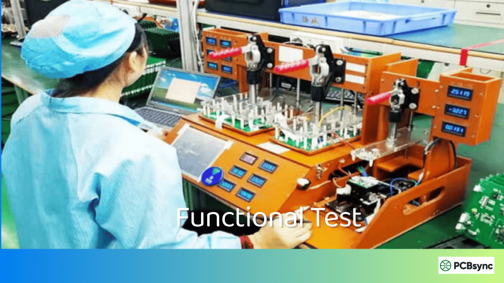
Functional Tester: To perform powered testing during and after stress
Monitoring System: Data acquisition for temperature, vibration levels, and test results
The chamber selection is critical. Don’t confuse ESS chambers with standard environmental test chambers—they’re optimized for very different purposes. ESS chambers prioritize fast temperature transition rates and uniform air distribution over precise temperature control at static conditions.
Monitoring and Optimization
ESS is not a “set it and forget it” process. Effective programs include:
Failure Tracking: Log every failure with detailed failure analysis. You should see a decreasing failure rate as screening removes weak units. If failures plateau at a high level, you have a systemic manufacturing problem.
Process Feedback: ESS data feeds back into manufacturing. A spike in solder joint failures might indicate a reflow oven problem. Connector failures might point to assembly training issues.
Screen Optimization: Start with conservative parameters (e.g., 30 temperature cycles) and monitor failure data. If your last failures occur at cycle 15, you can potentially reduce to 20 cycles without sacrificing effectiveness. This optimization reduces screening costs and improves throughput.
Military Standards and Industry Guidelines
ESS requirements and methodologies are well-documented in several key standards:
Military Standards
Standard
Title
Application
MIL-HDBK-344A
Environmental Stress Screening of Electronic Equipment
Primary ESS guidance document
MIL-STD-810G
Environmental Engineering Considerations and Laboratory Tests
Environmental test methods
MIL-STD-2164
Environment Stress Screening Process for Electronic Equipment
ESS procedures
MIL-STD-883H
Test Methods for Microelectronics
Component-level screening
MIL-HDBK-781A
Reliability Test Methods, Plans, and Environments
Reliability demonstration
Industry Standards
Standard
Organization
Focus
IEST-RP-PR001
IEST
ESS process management guidelines
IPC-9592A
IPC
Requirements for Power Conversion Devices
SR-332
Telcordia
Reliability prediction procedures
RTCA DO-160
RTCA
Environmental conditions for airborne equipment
For commercial products, the IEST-RP-PR001 guideline provides an excellent framework. It doesn’t mandate specific parameters but establishes the methodology for developing and optimizing your screening process.
Cost-Benefit Analysis: Is ESS Worth It?
Let’s address the elephant in the room: ESS costs money. Equipment, floor space, cycle time, and potential yield loss all impact your bottom line. But the alternative—field failures—costs more.
Consider a typical cost breakdown:
Cost Category
Without ESS
With ESS
ESS Equipment (amortized)
$0
$15-50 per unit
Field Service Call
$500-2000
Avoided
Warranty Replacement
Full unit cost
Avoided
Customer Dissatisfaction
Lost future sales
Maintained reputation
Recall Risk
Potential liability
Greatly reduced
The break-even calculation is straightforward. If your ESS cost is $25 per unit and your field service cost is $500, you break even if ESS prevents more than 5% of units from becoming field failures. Most ESS programs catch significantly more than that.
The math gets even more compelling for high-reliability applications (aerospace, medical, industrial) where field failures can cost thousands of dollars or create safety risks.
Useful Resources for ESS Implementation
Here are resources I recommend for anyone implementing or improving an ESS program:
Frequently Asked Questions About Environmental Stress Screening
What is the difference between ESS and burn-in testing?
Burn-in is actually a subset of ESS. Traditional burn-in typically involves operating a product at elevated temperature for an extended period (often 24-168 hours) to precipitate early failures. ESS is a broader term that includes temperature cycling, vibration, and other stresses in addition to or instead of simple burn-in. Modern ESS programs using temperature cycling are generally more effective than static burn-in—a 1990 Motorola study found that simple burn-in removed very few failures that wouldn’t have been caught by standard testing, while temperature cycling was far more effective at precipitating latent defects.
How long should an ESS process take?
It depends on your stress levels and product characteristics. Traditional ESS using conservative parameters might require 20-30 temperature cycles taking 12-24 hours. HASS programs using higher stress levels can achieve equivalent screening in 1-4 hours. The key is monitoring your failure data—start with baseline parameters from industry guidelines, then optimize based on when failures actually occur. If your last failure consistently happens before cycle 15, running 30 cycles is wasting time and money.
Does ESS damage good products?
When properly designed, ESS should not consume significant life from good products. The stress levels are chosen to be below the product’s design limits, so properly manufactured units experience the screening as normal operation within their capabilities. However, there is some life consumption—typically estimated at less than 1% of useful life for well-designed screens. This is why HALT is valuable: by knowing your actual operating limits, you can design HASS screens that maximize defect precipitation while minimizing life consumption on good units.
Can ESS be eliminated if our manufacturing process is mature?
Theoretically, yes. If your manufacturing process is so well-controlled that defect rates approach zero, ESS provides diminishing returns. Some high-volume consumer electronics manufacturers have reduced or eliminated ESS by achieving extremely tight process control. However, for most applications—especially aerospace, medical, and industrial—the consequences of field failures are severe enough that ESS remains standard practice regardless of process maturity. The insurance value alone often justifies the cost.
What happens if a unit fails during ESS?
That’s exactly what you want to happen—better in your factory than in your customer’s application. Failed units are removed from production and undergo failure analysis to determine root cause. This information feeds back into your manufacturing process for corrective action. The failed unit might be repaired (if economically justified) and re-screened, or scrapped. Either way, you’ve prevented a field failure and gained valuable information about your manufacturing process health.
Common Mistakes to Avoid in ESS Implementation
Over the years, I’ve seen plenty of ESS programs fail to deliver expected results. Here are the most common pitfalls:
Using inadequate temperature transition rates. Many facilities try to use standard environmental chambers for ESS. These chambers are designed for slow, precise temperature control—not the rapid transitions ESS requires. If your chamber can’t achieve at least 5°C/minute, you’re not doing effective ESS.
Ignoring air velocity. Temperature transition rate means nothing if the product itself isn’t changing temperature. Poor air circulation means the chamber air hits setpoint while the product is still 20°C behind. Aim for at least 750 ft/minute across all products.
Setting temperature ranges too conservatively. I’ve reviewed ESS programs using 25°C to 50°C ranges when components were rated for -40°C to +85°C. Wider ranges mean more thermal stress and more effective screening. Use your component ratings.
Skipping failure analysis. Every ESS failure is a learning opportunity. If you’re just scrapping failed units without understanding why they failed, you’re missing half the value of your ESS program.
Not integrating with manufacturing feedback. ESS data should drive process improvements. If solder joint failures spike after a reflow oven maintenance event, that’s actionable intelligence.
Taking Your ESS Program to the Next Level
Environmental Stress Screening isn’t glamorous. It doesn’t generate patents or press releases. But after years of working with electronic assemblies, I can tell you that ESS is one of the highest-ROI quality investments you can make.
The key is treating ESS as a process, not a test. It should be continuously monitored, optimized, and integrated with your broader quality system. The failure data you generate is gold—use it to drive manufacturing improvements, not just screen out bad units.
If you’re just starting out, begin with conservative parameters based on industry guidelines and your component temperature limits. Track every failure meticulously. After you have enough data, start optimizing—reduce cycle counts where justified, adjust temperature ranges, and consider transitioning to HASS if you’ve done HALT on your design.
The products that survive a well-designed ESS program represent your true manufacturing capability. They’re the units your customers will actually receive. And they’ll perform reliably in the field because you’ve already removed the weak links in your factory—exactly where you want to find them.
Inquire: Call 0086-755-23203480, or reach out via the form below/your sales contact to discuss our design, manufacturing, and assembly capabilities.
Quote: Email your PCB files to Sales@pcbsync.com (Preferred for large files) or submit online. We will contact you promptly. Please ensure your email is correct.
Notes: For PCB fabrication, we require PCB design file in Gerber RS-274X format (most preferred), *.PCB/DDB (Protel, inform your program version) format or *.BRD (Eagle) format. For PCB assembly, we require PCB design file in above mentioned format, drilling file and BOM. Click to download BOM template To avoid file missing, please include all files into one folder and compress it into .zip or .rar format.


