Inquire: Call 0086-755-23203480, or reach out via the form below/your sales contact to discuss our design, manufacturing, and assembly capabilities.
Quote: Email your PCB files to Sales@pcbsync.com (Preferred for large files) or submit online. We will contact you promptly. Please ensure your email is correct.
Notes: For PCB fabrication, we require PCB design file in Gerber RS-274X format (most preferred), *.PCB/DDB (Protel, inform your program version) format or *.BRD (Eagle) format. For PCB assembly, we require PCB design file in above mentioned format, drilling file and BOM. Click to download BOM template To avoid file missing, please include all files into one folder and compress it into .zip or .rar format.
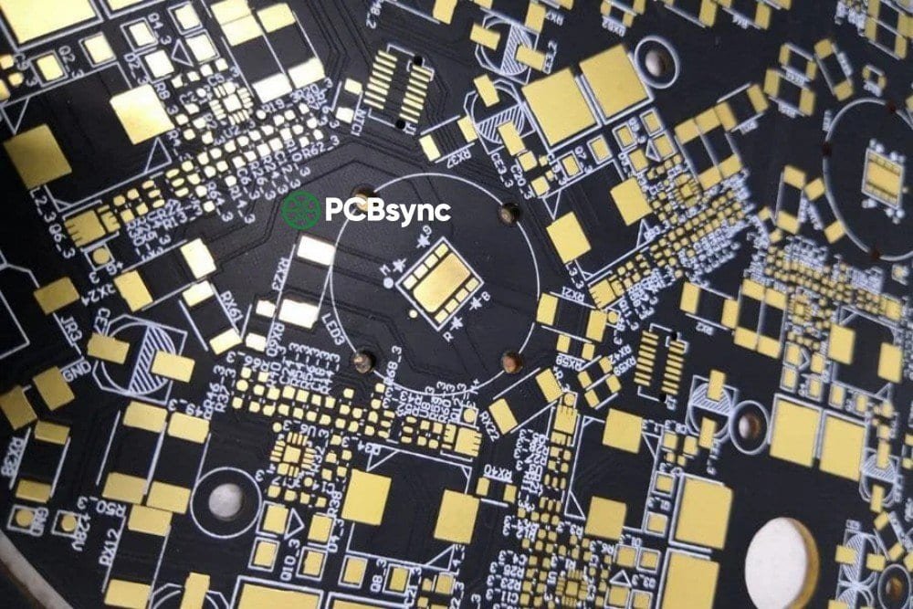
If you’ve ever worked on a PCB design that requires fine-pitch components, BGA packages, or simply needs to survive more than a few months on the shelf before assembly, chances are you’ve encountered ENIG. As a PCB engineer who has specified surface finishes for everything from consumer gadgets to medical devices, I can tell you that understanding ENIG isn’t just academic—it directly impacts whether your boards will solder properly and function reliably in the field.
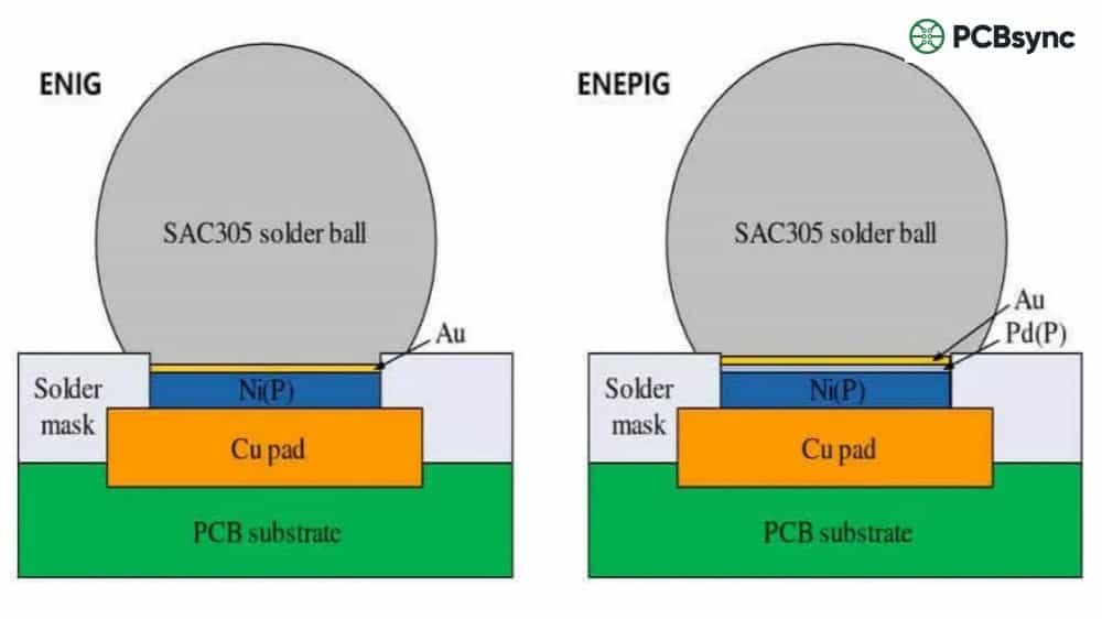
ENIG stands for Electroless Nickel Immersion Gold. It’s a two-layer metallic surface finish consisting of a nickel layer (typically 3-6 μm thick) deposited through an autocatalytic chemical process, followed by a thin gold layer (0.05-0.23 μm) applied through an immersion displacement reaction. The nickel acts as a barrier protecting the copper from oxidation and provides the actual soldering surface, while the gold prevents the nickel from oxidizing during storage and handling.
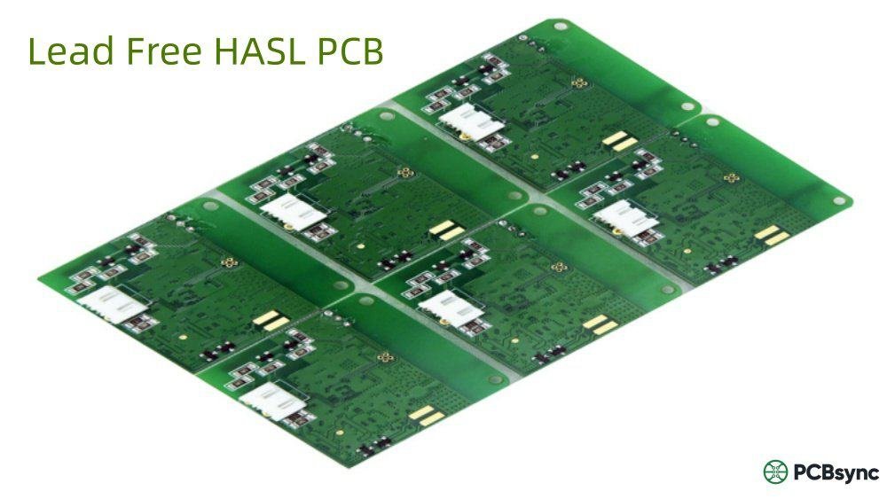
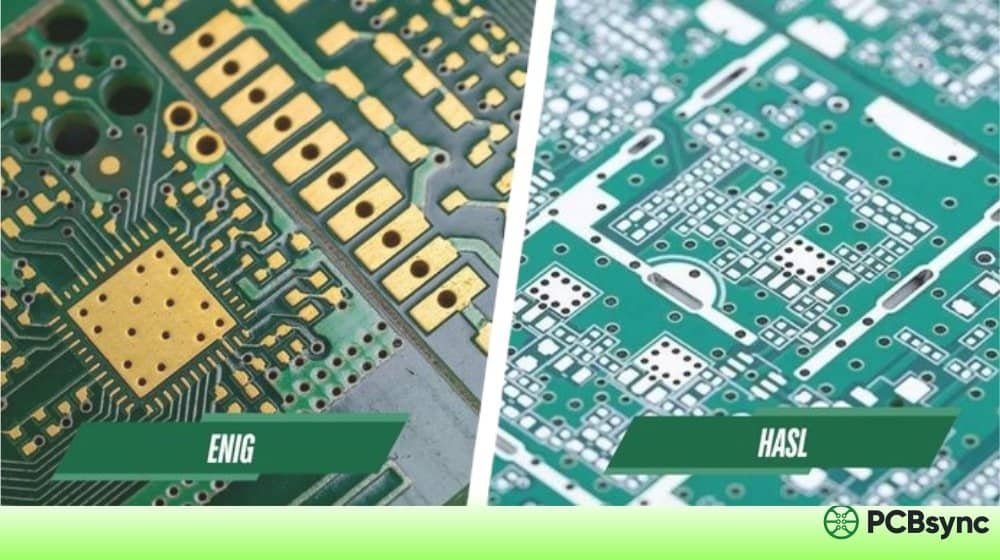
Unlike older finishes like HASL (Hot Air Solder Leveling), ENIG produces an exceptionally flat surface—critical when you’re placing 0.4mm pitch BGAs or working with chip-scale packages. This guide covers everything you need to know about ENIG PCB surface finish: how it works, when to use it, its advantages and limitations, and practical considerations from real-world manufacturing.
Before diving deep into ENIG, let’s step back and consider why surface finishes exist in the first place. Copper oxidizes. It’s that simple. Leave bare copper exposed to air for even a few days, and you’ll start seeing tarnish that makes soldering difficult or impossible.
A surface finish serves two essential functions:
Protecting copper from oxidation during storage, shipping, and handling
Providing a solderable surface when it’s time to attach components
The choice of finish affects solderability, shelf life, cost, flatness, and compatibility with specific assembly processes. Get it wrong, and you’re looking at rework, scrap, or field failures.
How the ENIG Process Works
The ENIG plating process involves multiple carefully controlled chemical steps. Here’s what actually happens on the production floor:
Step 1: Surface Preparation
The process begins with thorough cleaning of the copper surfaces. This includes alkaline cleaning to remove organic contaminants, micro-etching to create a fresh copper surface with proper topography for adhesion, and acid dipping to remove any residual oxides. Skipping or rushing this step is a recipe for adhesion problems later.
Step 2: Activation
A palladium-based catalyst is applied to the clean copper surface. This activator initiates the electroless nickel deposition in the next step. The palladium essentially provides nucleation sites where the nickel reduction reaction can begin.
Step 3: Electroless Nickel Deposition
This is where the “electroless” part comes in. Unlike electroplating, no external electrical current is applied. Instead, a chemical reducing agent in the nickel bath reduces nickel ions directly onto the activated copper surface through an autocatalytic reaction. The nickel-phosphorus alloy (typically 7-9% phosphorus content for mid-phos) builds up to the target thickness of 3-6 micrometers.
Step 4: Immersion Gold Deposition
The nickel-plated board is then immersed in a gold solution. Through a displacement reaction, gold ions replace nickel atoms at the surface, creating a thin protective gold layer. This reaction is self-limiting—once the gold completely covers the nickel surface, the reaction essentially stops. That’s why immersion gold layers are inherently thin (0.05-0.23 μm).
Step 5: Rinsing and Drying
Final rinse steps remove any residual chemicals, and the board is dried. At this point, the ENIG finish is complete and the board is ready for inspection, testing, and shipment.
The IPC-4552 standard governs ENIG specifications. Here are the key parameters:
Layer
Minimum Thickness
Typical Range
Maximum Thickness
Electroless Nickel
3 μm (120 μin)
3-6 μm (120-240 μin)
6 μm (240 μin)
Immersion Gold
0.05 μm (2 μin)
0.075-0.125 μm (3-5 μin)
0.23 μm (9 μin)
Phosphorus Content
7%
7-9% (mid-phos)
9%
The latest revision, IPC-4552B (released April 2021), added significant detail around corrosion evaluation and introduced product rating systems to help identify and prevent black pad issues—more on that later.
Advantages of ENIG PCB Surface Finish
Excellent Surface Planarity
ENIG produces one of the flattest surface finishes available. This is crucial for fine-pitch components where even slight surface irregularities can cause solder bridging or insufficient solder joints. If you’re working with 0.4mm or 0.5mm pitch BGAs, ENIG is often your only practical choice.
Superior Shelf Life
Properly processed ENIG maintains solderability for 12 months or more under appropriate storage conditions. The gold layer provides outstanding oxidation protection for the underlying nickel. This matters when you’re building boards for products that might sit in inventory before final assembly.
Excellent Solderability
Both nickel and gold wet well with standard solder alloys. During reflow, the thin gold layer dissolves into the solder, and a proper intermetallic compound (IMC) forms between the tin and nickel. This creates strong, reliable solder joints.
Wire Bonding Compatibility
ENIG is suitable for gold wire bonding applications, making it a good choice for chip-on-board (COB) assemblies and semiconductor packaging. The gold surface provides the clean, bondable interface required for successful wire bonds.
RoHS Compliance
ENIG contains no lead or other restricted substances under RoHS (Restriction of Hazardous Substances) directives. As the industry continues moving away from lead-based finishes, ENIG remains fully compliant with environmental regulations.
Compatibility with Multiple Solder Alloys
Whether you’re using traditional Sn63/Pb37, SAC305 (lead-free), or other alloys, ENIG works well across the board. This flexibility is valuable when manufacturing for different markets or transitioning between solder types.
ENIG PCB Disadvantages and Challenges
Higher Cost
ENIG costs more than HASL, OSP, or immersion tin. The multi-step chemical process and use of precious metals (gold, palladium in the activator) drive up processing costs. For high-volume, cost-sensitive products, this can be a significant factor.
Black Pad Syndrome
This is the elephant in the room when discussing ENIG. Black pad occurs when the nickel layer corrodes during the gold deposition process, leaving a phosphorus-rich, non-solderable surface beneath the gold. You typically don’t discover black pad until assembly—or worse, until field failures start appearing.
IPC-4552B introduced detailed corrosion evaluation criteria and product rating systems specifically to address black pad:
Product Rating
Criteria
Acceptability
Rating 0
No corrosion defects observed
Acceptable
Rating 1
>60% of locations show Level 1 or less
Acceptable
Rating 2
Defects > Rating 1, < Rating 3
Acceptable if solderability passes
Rating 3
>40% of locations show Level 3 defects
Non-conforming
Not Ideal for Multiple Reflow Cycles
While ENIG can handle typical SMT reflow processes, it’s not the best choice for boards requiring many thermal excursions. After 3-4 reflow cycles, solderability can degrade. If your assembly process involves multiple reflows or extensive rework, consider this limitation.
Signal Loss at Very High Frequencies
For RF applications above several GHz, the nickel layer can introduce signal loss due to its magnetic properties and skin effect behavior. In these cases, finishes like immersion silver or specialized RF surface treatments may perform better.
ENIG vs Other PCB Surface Finishes
Feature
ENIG
HASL
OSP
Immersion Silver
ENEPIG
Surface Flatness
Excellent
Poor
Good
Good
Excellent
Shelf Life
12+ months
12+ months
3-6 months
6-12 months
12+ months
Cost
High
Low
Low
Medium
Very High
Fine Pitch Capability
Excellent
Poor
Good
Good
Excellent
Wire Bonding
Yes
No
No
No
Excellent
RoHS Compliant
Yes
Lead-free only
Yes
Yes
Yes
Black Pad Risk
Moderate
None
None
None
Very Low
Multiple Reflows
Limited
Good
Limited
Good
Good
When to Choose ENIG Over Alternatives
Choose ENIG when your design requires:
Fine-pitch components (0.5mm pitch or less)
BGA or CSP packages
Long shelf life before assembly
Gold wire bonding capability
Lead-free, RoHS-compliant manufacturing
Flat landing pads for SMT placement accuracy
Consider alternatives when:
Budget is extremely constrained (use HASL or OSP)
RF performance above 3-5 GHz is critical (consider immersion silver)
Maximum reflow reliability is needed (consider ENEPIG)
Black pad risk must be absolutely minimized (consider ENEPIG)
ENIG PCB Applications by Industry
Consumer Electronics
Smartphones, tablets, laptops, wearables, and gaming devices commonly use ENIG. The finish supports the high-density designs and fine-pitch components typical in consumer products, while meeting RoHS requirements for products sold globally.
Telecommunications
Network equipment, routers, base stations, and communication infrastructure benefit from ENIG’s reliability and signal integrity. The flat surface supports high-speed digital circuits common in telecom applications.
Medical Devices
Medical electronics—diagnostic equipment, monitoring devices, implantables, and imaging systems—require the highest reliability. ENIG’s consistent solderability and corrosion resistance make it a standard choice for medical PCBs where failure is not an option.
Automotive Electronics
Engine control units, infotainment systems, ADAS sensors, and EV power electronics increasingly rely on ENIG. The automotive environment demands finishes that can withstand temperature extremes, vibration, and long service life.
Aerospace and Defense
Mission-critical aerospace electronics require proven reliability under extreme conditions. ENIG’s track record and compliance with military specifications make it suitable for avionics, satellite systems, and defense electronics.
Industrial Controls
PLCs, motor drives, HMIs, and automation equipment use ENIG for its reliability in factory environments where downtime is costly and replacement is difficult.
Best Practices for Specifying ENIG PCB
Work with Qualified Suppliers
Not all ENIG processes are equal. Work with fabricators who:
Follow IPC-4552B specifications
Have documented process controls for their nickel and gold baths
Can provide corrosion evaluation data when requested
Have a track record with your type of product
Specify Appropriate Thickness
Don’t blindly accept default specifications. Consider your application:
For standard SMT assembly: 3-5 μm nickel, 0.05-0.1 μm gold
For wire bonding: May require thicker gold (consult your bonder requirements)
For harsh environments: Consider thicker nickel for additional protection
Control Storage Conditions
Even though ENIG has excellent shelf life, proper storage extends it further:
Store in sealed moisture barrier bags with desiccant
Control temperature and humidity (ideally below 30°C, 60% RH)
Minimize handling to avoid contamination
Track shelf life and use FIFO inventory management
Validate Incoming Quality
For critical applications, consider incoming inspection:
Visual inspection for discoloration or contamination
XRF thickness measurement on sample boards
Solderability testing per J-STD-003
Useful Resources and Standards
When working with ENIG PCBs, these resources provide essential reference information:
Resource
Description
Access
IPC-4552B
ENIG specification for thickness, corrosion evaluation
Sierra Circuits Knowledge Base – Practical surface finish guides
Uyemura Technical Resources – Chemistry and process details from a major ENIG supplier
IPC Validation Services – Third-party testing and certification
Frequently Asked Questions
What does ENIG stand for and how is it different from immersion gold?
ENIG stands for Electroless Nickel Immersion Gold. The terms are often used interchangeably in the industry, though technically “immersion gold” refers specifically to the gold deposition step. ENIG describes the complete two-layer finish: the electroless nickel barrier layer plus the protective immersion gold layer. When someone asks for “immersion gold” on their PCB, they typically mean ENIG.
How long can ENIG PCBs be stored before assembly?
Under proper storage conditions (sealed moisture barrier bags with desiccant, controlled temperature and humidity), ENIG PCBs maintain solderability for 12 months or longer. Some manufacturers report acceptable solderability beyond 24 months. However, I recommend using boards within 12 months and always performing solderability verification if boards have been stored longer or under uncertain conditions.
What causes black pad in ENIG and how can it be prevented?
Black pad results from hyper-corrosion of the nickel layer during immersion gold deposition. The gold displacement reaction attacks the nickel surface, leaving behind a phosphorus-rich, non-solderable layer. Contributing factors include excessive phosphorus content in the nickel (too high or too low), overly aggressive gold bath chemistry, inadequate process control, and contamination. Prevention requires strict process control: maintaining proper nickel bath chemistry (7-9% phosphorus), controlling gold bath pH (4.5-5.5), using appropriate immersion times, and working with suppliers who follow IPC-4552B guidelines.
Is ENIG suitable for high-frequency RF applications?
ENIG works well for most RF applications up to several GHz. However, at very high frequencies (above 5-6 GHz), the nickel layer can introduce additional insertion loss due to its magnetic properties and the skin effect. For mmWave applications or extremely loss-sensitive RF designs, immersion silver or specialized RF finishes may offer better performance. Always consult your RF engineer and consider simulation or prototype testing for critical high-frequency designs.
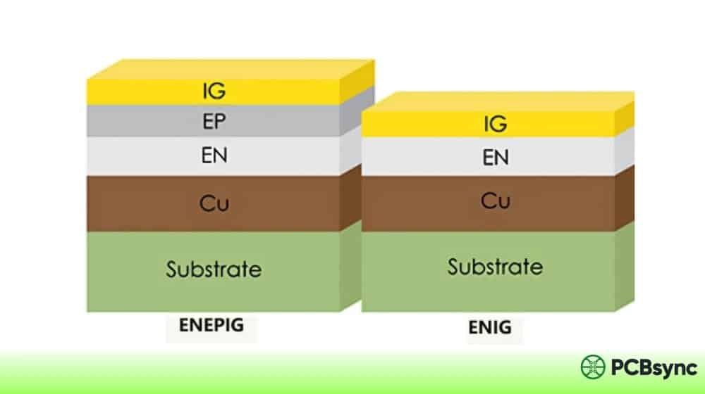
What’s the difference between ENIG and ENEPIG, and when should I use each?
ENEPIG (Electroless Nickel Electroless Palladium Immersion Gold) adds a thin palladium layer between the nickel and gold. This palladium barrier virtually eliminates black pad risk because it prevents the gold displacement reaction from attacking the nickel directly. ENEPIG also offers superior wire bonding performance (both gold and aluminum wire) and better solder joint reliability through multiple reflow cycles. Use ENIG for standard applications where cost matters and black pad risk is acceptable with proper process control. Choose ENEPIG for high-reliability applications (aerospace, medical, automotive safety systems), designs requiring wire bonding, or when you’ve experienced black pad issues with ENIG.
Conclusion
ENIG remains one of the most versatile and widely used PCB surface finishes in the electronics industry. Its combination of excellent surface planarity, reliable solderability, long shelf life, and RoHS compliance makes it suitable for everything from consumer electronics to aerospace applications. While it costs more than basic finishes like HASL or OSP and carries some risk of black pad defects, proper specification and supplier qualification mitigate these concerns for most applications.
When designing your next PCB, consider whether your requirements—fine-pitch components, BGA packages, shelf life needs, wire bonding, assembly compatibility—point toward ENIG. If they do, work with qualified fabricators who follow IPC-4552B standards and maintain rigorous process control. The extra investment in a quality ENIG finish pays dividends in assembly yields, reliability, and customer satisfaction.
For designs demanding the absolute highest reliability or where black pad risk must be minimized, consider upgrading to ENEPIG. But for the vast majority of PCB applications, ENIG delivers the performance engineers need at a reasonable cost.
Inquire: Call 0086-755-23203480, or reach out via the form below/your sales contact to discuss our design, manufacturing, and assembly capabilities.
Quote: Email your PCB files to Sales@pcbsync.com (Preferred for large files) or submit online. We will contact you promptly. Please ensure your email is correct.
Notes: For PCB fabrication, we require PCB design file in Gerber RS-274X format (most preferred), *.PCB/DDB (Protel, inform your program version) format or *.BRD (Eagle) format. For PCB assembly, we require PCB design file in above mentioned format, drilling file and BOM. Click to download BOM template To avoid file missing, please include all files into one folder and compress it into .zip or .rar format.


