Inquire: Call 0086-755-23203480, or reach out via the form below/your sales contact to discuss our design, manufacturing, and assembly capabilities.
Quote: Email your PCB files to Sales@pcbsync.com (Preferred for large files) or submit online. We will contact you promptly. Please ensure your email is correct.
Notes: For PCB fabrication, we require PCB design file in Gerber RS-274X format (most preferred), *.PCB/DDB (Protel, inform your program version) format or *.BRD (Eagle) format. For PCB assembly, we require PCB design file in above mentioned format, drilling file and BOM. Click to download BOM template To avoid file missing, please include all files into one folder and compress it into .zip or .rar format.
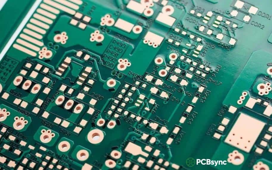
If you’ve spent any time selecting surface finishes for high-reliability PCBs, you’ve probably wrestled with the same question I have: which finish actually delivers on its promises without breaking the budget or creating assembly headaches down the line?
After years of working with various surface treatments, I’ve come to appreciate why ENEPIG (Electroless Nickel Electroless Palladium Immersion Gold) has earned the nickname “universal finish.” It’s not just marketing speak—this surface treatment genuinely solves problems that other finishes simply can’t address.
In this guide, I’ll walk you through everything you need to know about ENEPIG: what it is, how it works, when you should (and shouldn’t) use it, and how it stacks up against alternatives like ENIG. Whether you’re designing boards for aerospace applications or trying to prevent black pad failures on your BGA substrates, this article will give you the practical knowledge to make informed decisions.
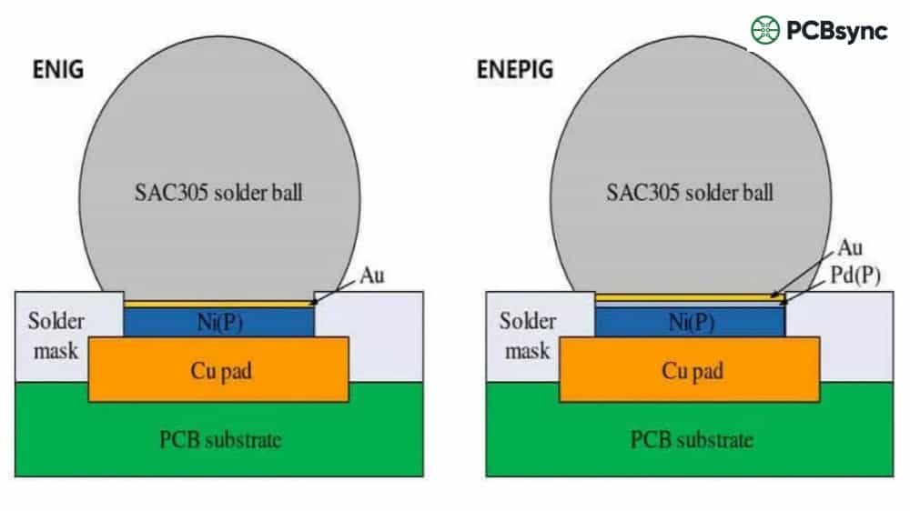
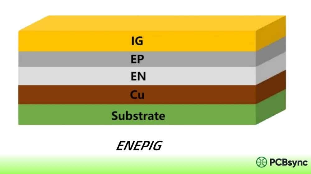
ENEPIG stands for Electroless Nickel Electroless Palladium Immersion Gold. It’s a multi-layer surface finish applied to PCB copper pads to protect them from oxidation while providing excellent solderability and wire bonding capability.
What makes ENEPIG unique is its four-layer structure built on top of the copper base:
Copper (Cu) – The PCB trace foundation
Electroless Nickel (Ni-P) – 3-6 μm thick; acts as a diffusion barrier and solderable surface
Immersion Gold (Au) – 0.03-0.05 μm thick; protects palladium from oxidation and provides contact surface
Intel originally developed this process back in the late 1990s, though it took years for the industry to widely adopt it. The main barrier was palladium pricing—back in the early 2000s, palladium was actually more expensive than gold, which made ENEPIG economically impractical for most applications.
Today, palladium prices have stabilized at roughly one-third the cost of gold, making ENEPIG a genuinely cost-effective alternative to thick gold plating while delivering superior performance for demanding applications.
IPC-4556 Thickness Specifications
The IPC-4556 specification (released in January 2013) establishes the industry standard for ENEPIG thickness requirements. Here’s what you need to know:
Layer
Thickness Range
Function
Electroless Nickel
3-6 μm
Diffusion barrier, solderable surface
Electroless Palladium
0.05-0.15 μm
Corrosion barrier, wire bonding surface
Immersion Gold
0.03-0.05 μm (max 0.07 μm)
Oxidation protection, contact surface
These thickness specifications matter because both too-thin and too-thick layers create problems. Palladium that’s too thin won’t adequately protect the nickel from corrosion, while palladium that’s too thick can make solder joints brittle.
The ENEPIG Process: How It Works
Understanding how ENEPIG is applied helps you appreciate why it performs the way it does—and why process control is so critical. Here’s the step-by-step breakdown:
Step 1: Copper Activation
The process begins with thorough cleaning and micro-etching of the copper surface. This removes oxides and contaminants while creating a slightly roughened surface that promotes adhesion. A displacement reaction then activates the copper, making it act as a catalytic surface for the subsequent plating steps.
Step 2: Electroless Nickel Deposition
Nickel is deposited through an electroless (autocatalytic) process using an oxidation-reduction reaction. The nickel layer serves as the primary diffusion barrier, preventing copper from migrating into the upper layers. This layer is actually a nickel-phosphorus alloy, with phosphorus content typically between 7-11%—a detail that becomes important when we discuss black pad prevention.
Step 3: Electroless Palladium Deposition
This is what distinguishes ENEPIG from ENIG. The palladium layer is deposited through another electroless reaction, creating a thin but critical barrier between the nickel and gold. Palladium prevents nickel from corroding during the gold immersion step and stops nickel atoms from diffusing into the gold layer over time.
Step 4: Immersion Gold Plating
The final gold layer is applied through immersion plating—a displacement reaction where palladium atoms on the surface are replaced by gold atoms from the plating solution. This self-limiting process produces a very thin but uniform gold layer that protects the palladium from oxidation and provides an excellent contact surface.
Step 5: Rinsing and Inspection
Complete drying is essential—any residual moisture can cause spotting or oxidation. Final inspection includes visual examination and X-ray fluorescence (XRF) measurements to verify layer thicknesses meet IPC-4556 requirements.
So why would you choose ENEPIG over simpler, cheaper alternatives? Here are the technical reasons that matter:
1. Eliminates Black Pad Syndrome
This is probably the single biggest advantage for anyone who’s dealt with ENIG failures. Black pad occurs when the immersion gold process aggressively attacks the nickel layer, causing hyper-corrosion at grain boundaries. The result? Brittle solder joints that look fine during inspection but fail catastrophically under stress.
With ENEPIG, the palladium layer acts as a diffusion barrier, physically preventing the gold from directly attacking the nickel. There’s simply no possibility of grain boundary corrosion because the two metals never come into direct contact during plating.
2. Superior Wire Bonding Performance
ENEPIG supports both gold and aluminum wire bonding with excellent reliability—something ENIG struggles with. The palladium layer enables thicker gold deposits (up to 6-7 micro-inches versus ENIG’s self-limiting 2-3 micro-inches) and provides a clean, consistent bonding surface.
Research shows that ENEPIG maintains high pull strengths even after 1000+ hours of thermal aging, making it the finish of choice for chip-on-board (COB) and other wire-bonded assemblies.
3. Excellent Solderability
ENEPIG provides outstanding solder wetting characteristics with both leaded and lead-free solders. During reflow, the thin palladium layer completely dissolves into the solder, leaving a clean oxide-free nickel surface that forms reliable tin-nickel intermetallics.
Critically, ENEPIG withstands multiple reflow cycles without degradation—essential for double-sided assembly or rework operations.
4. Long Shelf Life
ENEPIG-finished boards maintain solderability for 12-18 months under proper storage conditions (30°C, 60% RH). This exceeds ENIG’s typical 6-12 month shelf life and far surpasses OSP’s limited storage window.
5. RoHS Compliance
ENEPIG is fully lead-free and complies with RoHS and WEEE directives. Unlike some alternatives, it performs exceptionally well with lead-free solders that require higher reflow temperatures.
6. Low Contact Resistance
The uniform deposition process creates consistent electrical resistance across the surface—easier to predict and manage for impedance-controlled designs. ENEPIG also works well for touch interfaces and membrane switch contacts.
ENEPIG vs ENIG: Head-to-Head Comparison
Since ENEPIG evolved from ENIG, it’s natural to compare them directly. Here’s how they stack up:
Feature
ENIG
ENEPIG
Layer Structure
Ni (3-6 μm) + Au (0.05-0.1 μm)
Ni (3-6 μm) + Pd (0.05-0.15 μm) + Au (0.03-0.05 μm)
Black Pad Risk
Yes – requires careful process control
No – palladium prevents nickel corrosion
Gold Wire Bonding
Poor – not recommended
Excellent – industry standard
Aluminum Wire Bonding
Good for Al wedge bonding
Excellent for both Al and Au
Solderability
Good
Excellent
Multiple Reflow Cycles
Limited
Excellent – withstands many cycles
Shelf Life
6-12 months
12-18 months
Relative Cost
Lower (no palladium)
Higher (15-30% premium)
Best Applications
Consumer electronics, standard SMT
Wire bonding, high-reliability, mixed assembly
Recent reliability studies show that ENEPIG-coated PCBs can exhibit up to 30% higher reliability in extreme temperature cycling tests (-40°C to 125°C) compared to ENIG, primarily due to the elimination of black pad failures.
When to Choose ENIG Instead
ENIG remains a solid choice for cost-sensitive applications that don’t require wire bonding. Consumer electronics, standard SMT assemblies, and prototype work often don’t justify ENEPIG’s cost premium. If your application operates in controlled environments with limited thermal cycling, ENIG provides good value.
ENEPIG vs Other Surface Finishes
Beyond ENIG, how does ENEPIG compare to the full range of surface finish options?
Finish
Cost
Solderability
Wire Bonding
Shelf Life
ENEPIG
$$$
Excellent
Excellent
12-18 months
ENIG
$$
Good
Poor
6-12 months
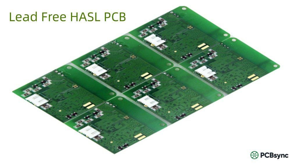
HASL (Lead-Free)
$
Good
None
12+ months
Immersion Silver
$$
Excellent
None
6-12 months
OSP
$
Good
None
3-6 months
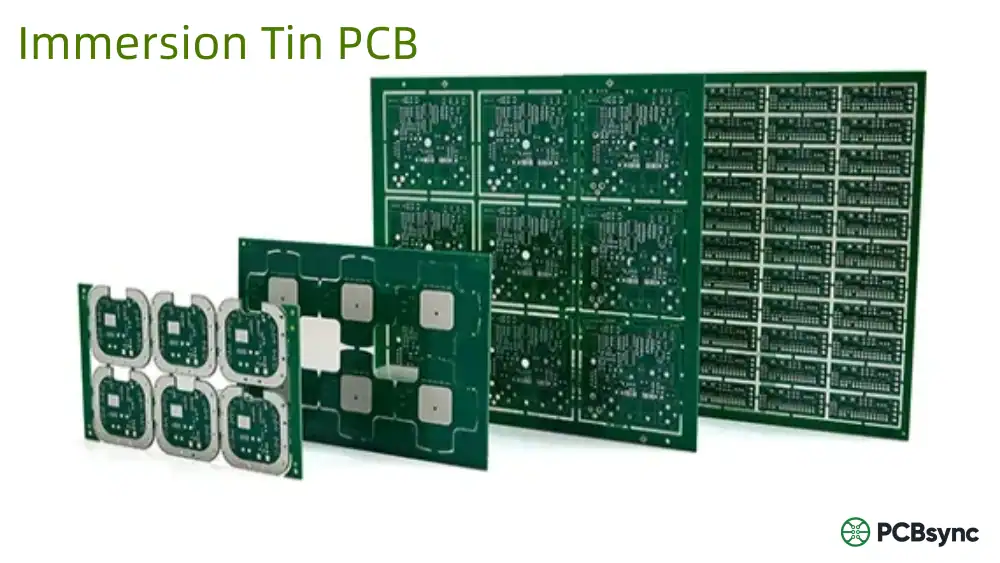
Immersion Tin
$
Good
None
6 months
Hard Gold
$$$$
Poor
Good
Indefinite
ENEPIG occupies a unique position as the only surface finish that provides both excellent solderability AND wire bonding capability. This is why it’s called the “universal finish”—it supports virtually every assembly method.
When to Use ENEPIG: Ideal Applications
ENEPIG shines in applications where reliability is non-negotiable or where multiple assembly technologies coexist on the same board:
High-Reliability Industries
Aerospace and Defense: Avionics, radar systems, and military electronics where environmental stresses (humidity, salt spray, thermal cycling) demand maximum corrosion resistance
Medical Devices: Implantables, diagnostic equipment, and patient monitoring systems where failure is not an option
Automotive Electronics: Engine control units (ECUs), ADAS modules, and EV power systems that face extreme temperature swings
Technical Requirements
Wire Bonding Applications: Gold ball bonding for chip-on-board (COB), aluminum wedge bonding for power devices
BGA and Fine-Pitch Components: The flat, uniform surface is ideal for 0.4mm pitch BGAs and smaller
HDI (High-Density Interconnect) Boards: Compatible with microvias and fine traces
Mixed Technology Boards: Combines RF and digital circuits, soldering and wire bonding on the same board
Multiple Reflow Operations: Double-sided assembly or boards requiring rework
Component Packages
ENEPIG is particularly well-suited for advanced packaging technologies including BGA, QFN, CSP, flip-chip, and system-in-package (SiP) designs where both soldering and wire bonding may be required.
Limitations and Considerations
ENEPIG isn’t the right choice for every application. Here are the trade-offs you need to consider:
Cost Premium
ENEPIG typically costs 15-30% more than ENIG due to the additional palladium layer and more complex processing. For high-volume consumer products where reliability requirements are modest, this premium may not be justified. Industry pricing typically ranges from $45-80 per square meter, depending on volume and specifications.
Trace Spacing Considerations
The electroless nickel layer adds bulk to trace edges (3-6 μm on each side). For advanced PCBs with very tight trace spacing (<75 μm), this buildup can reduce clearance between conductors and increase short-circuit risk. In such cases, EPIG (Electroless Palladium Immersion Gold, without nickel) may be a better option.
Process Control Requirements
ENEPIG requires tighter process control than simpler finishes. Not all fabricators have the equipment and expertise to produce consistent results. Always verify your supplier’s ENEPIG capabilities and request test coupons before committing to production.
Palladium Price Volatility
While palladium prices have stabilized, they remain subject to market fluctuations. For long-term production programs, consider pricing agreements that account for potential commodity price changes.
Cost Analysis: Is ENEPIG Worth the Premium?
The cost question isn’t straightforward. While ENEPIG has higher upfront costs, you need to consider total cost of ownership:
Direct Cost Comparison
Surface Finish
Typical Cost per sq. meter
OSP
$15-25
Lead-Free HASL
$20-35
Immersion Silver
$25-40
ENIG
$35-55
ENEPIG
$45-80
Electrolytic Ni/Au
$80-150+
Note: Actual pricing varies significantly based on board complexity, volume, and supplier. These figures represent typical industry ranges.
Hidden Cost Savings
ENEPIG often delivers cost savings that don’t appear on the surface finish line item:
Reduced field failures (ENEPIG can cut failure rates by 40% or more in critical applications)
Lower rework costs (better first-pass yield)
Extended PCB lifespan (24+ months vs. 12 months for some alternatives)
Compared to electrolytic nickel/gold for wire bonding applications, ENEPIG offers 50-70% cost savings
The thinner gold layer in ENEPIG (enabled by palladium’s barrier properties) reduces precious metal consumption
How to Specify ENEPIG for Your Project
When ordering ENEPIG-finished PCBs, include these specifications in your fabrication notes:
Reference IPC-4556 for thickness requirements
Specify nickel thickness: 3-6 μm (typically 4-5 μm for best results)
Specify palladium thickness: 0.05-0.15 μm
Specify gold thickness: 0.03-0.05 μm
Request XRF thickness verification per IPC-4556 requirements
If wire bonding is required, specify pure palladium (without phosphorus co-deposition) for optimal results
Useful Resources for ENEPIG
Here are the key resources for further research and specification:
Industry Standards
IPC-4556: Specification for Electroless Nickel/Electroless Palladium/Immersion Gold (ENEPIG) Plating for Printed Circuit Boards – Available at shop.ipc.org
IPC-4552B: Performance Specification for Electroless Nickel/Immersion Gold (ENIG) Plating – For ENIG comparison reference
J-STD-003: Solderability Tests for Printed Boards – For solderability testing requirements
Technical Papers and Guides
“Wire Bonding and Soldering on ENEPIG and ENEP Surface Finishes with Pure Pd” – Available through SMTnet technical library
Fraunhofer IZM research papers on ENEPIG wire bonding reliability
Equipment and Testing
Hitachi High-Tech: XRF equipment guides for IPC-4556 compliance testing
Fischer Technology: XRF measurement recommendations for thin ENEPIG layers
Frequently Asked Questions
What does ENEPIG stand for?
ENEPIG stands for Electroless Nickel Electroless Palladium Immersion Gold. It describes the three metal layers deposited in sequence on copper PCB pads. The “electroless” designation indicates these layers are applied through autocatalytic chemical processes rather than electrolytic plating.
Is ENEPIG better than ENIG?
ENEPIG is technically superior in most performance metrics—it eliminates black pad risk, enables gold wire bonding, provides better solderability, and has a longer shelf life. However, “better” depends on your application. For standard SMT assembly in consumer electronics, ENIG may provide adequate performance at lower cost. For wire bonding, high-reliability, or harsh environment applications, ENEPIG is the clear choice.
Can ENEPIG be used for gold wire bonding?
Yes—this is one of ENEPIG’s primary advantages over ENIG. The palladium layer enables reliable gold ball bonding with 25μm wire, supporting both thermosonic and thermocompression bonding processes. ENEPIG also supports aluminum wedge bonding, making it suitable for power semiconductor packaging and chip-on-board assemblies.
How long is ENEPIG shelf life?
Under proper storage conditions (30°C, 60% RH), ENEPIG maintains excellent solderability for 12-18 months. Some manufacturers extend this to 24 months with vacuum packaging and desiccant. This exceeds ENIG’s typical 6-12 month shelf life and far surpasses OSP’s 3-6 month window.
Is ENEPIG RoHS compliant?
Yes, ENEPIG is fully RoHS and WEEE compliant. It contains no lead, mercury, cadmium, hexavalent chromium, PBB, or PBDE. The finish performs exceptionally well with lead-free solder alloys like SAC305, maintaining reliable solder joint formation even at higher reflow temperatures.
Supplier Selection Tips
Not all PCB fabricators are equally capable of producing high-quality ENEPIG finishes. When evaluating suppliers, ask these questions: How long have they been offering ENEPIG? What is their process control methodology? Can they provide test data showing consistent thickness measurements? Do they have experience with your specific application (wire bonding, high-frequency, etc.)? Request sample boards for evaluation before committing to production volumes.
Quality Control and Testing for ENEPIG
Ensuring consistent ENEPIG quality requires proper testing protocols. Here’s what you should know about verification methods:
XRF Thickness Measurement
X-ray fluorescence (XRF) is the IPC-approved method for measuring ENEPIG layer thicknesses. Per IPC-4556, the measurement spot size should not exceed 30% of the feature being measured. Proper calibration is critical—the very thin palladium and gold layers require precise equipment setup and validated reference standards.
Visual Inspection
Look for uniform golden color across all pads with no discoloration, staining, or spotting. Skip plating (areas where the gold didn’t properly cover) indicates process problems. IPC-4556 provides visual reference standards for acceptable finishes.
Solderability Testing
Test solderability per J-STD-003 requirements. ENEPIG should demonstrate excellent wetting with both leaded and lead-free solders. Any signs of de-wetting or poor solder spread indicate process issues that need investigation.
Cross-Section Analysis
For critical applications, cross-sectional analysis using SEM (Scanning Electron Microscopy) can verify layer structure and thickness. This destructive test is typically performed on coupon samples rather than production boards, but provides definitive verification of plating quality.
Troubleshooting Common ENEPIG Issues
Even with good process control, issues can arise. Here are common problems and their solutions:
Discoloration or Staining
Pink or brownish discoloration usually indicates incomplete gold coverage or contamination in the gold bath. This can result from inadequate rinsing between process steps or gold bath chemistry issues. Solution: Review rinse procedures and gold bath maintenance schedules.
Poor Wire Bonding
If wire bonding yields are lower than expected, check palladium thickness and purity. Palladium-phosphorus alloys (PdP) have different wire bonding characteristics than pure palladium. For optimal gold wire bonding, specify pure palladium deposition. Also verify surface cleanliness—any contamination will degrade bond strength.
Solderability Degradation
If solderability declines before the expected shelf life, investigate storage conditions. High humidity or temperature excursions can accelerate surface oxidation. Ensure boards are stored in controlled environments (< 30°C, < 60% RH) with desiccant when possible.
Thickness Out of Specification
Inconsistent layer thickness typically points to bath chemistry or process timing issues. Each plating step requires precise control of temperature, time, and chemical concentrations. Work with your fabricator to review and optimize process parameters.
Industry Adoption and Market Trends
ENEPIG adoption has accelerated significantly over the past decade. What was once a niche finish for specialized applications is now increasingly common in mainstream production. Several factors drive this trend: the rising cost of gold makes ENEPIG’s thin gold layer more attractive, lead-free assembly requirements favor finishes with excellent high-temperature performance, and the proliferation of fine-pitch BGAs demands flat, uniform surfaces that ENEPIG provides. Major semiconductor packaging facilities have standardized on ENEPIG for their BGA substrates, and this influence is rippling through the broader PCB industry.
Future Trends in ENEPIG Technology
The electronics industry continues to evolve, and ENEPIG technology is advancing alongside it:
Thinner Layers
Research is ongoing to reduce layer thicknesses while maintaining performance. Thinner deposits reduce material costs and are better suited for advanced HDI boards with extremely fine features. Expect continued refinement of IPC specifications to accommodate these thinner deposits.
Copper Wire Bonding
Copper wire bonding is gaining adoption as a cost-effective alternative to gold wire. Recent studies show that ENEP (ENEPIG without the final gold layer) with pure palladium can support copper wire bonding for IC substrate and PWB applications. This could open new application areas for the ENEPIG process family.
5G and High-Frequency Applications
As 5G deployment expands, demand for high-frequency PCBs is increasing. ENEPIG’s uniform surface finish and predictable impedance characteristics make it well-suited for RF applications. The palladium layer can also help mitigate nickel’s potential interference with high-frequency signals.
Sustainability Considerations
Environmental regulations continue to tighten globally. ENEPIG’s RoHS compliance and lead-free compatibility position it well for future regulatory requirements. Some research is exploring ways to reduce water usage and chemical waste in the plating process.
Conclusion
ENEPIG has earned its reputation as the “universal finish” by delivering what other surface treatments cannot: simultaneous excellence in solderability AND wire bonding, combined with superior corrosion resistance and long shelf life.
Is it the right choice for every project? No. For cost-sensitive consumer products with modest reliability requirements, simpler finishes like ENIG or OSP may suffice. But for aerospace, medical, automotive, or any application where failure isn’t an option, ENEPIG provides peace of mind that cheaper alternatives simply can’t match.
The key is matching the surface finish to your specific requirements. Consider your assembly methods, operating environment, reliability targets, and budget. When wire bonding is required, when black pad failures would be catastrophic, or when you need maximum process flexibility, ENEPIG delivers value that justifies its cost premium.
For PCB engineers working on high-reliability products, understanding ENEPIG isn’t optional—it’s essential knowledge for making informed design decisions. The surface finish may be a thin layer, but its impact on product performance and reliability is substantial.
As electronic devices continue to shrink while reliability demands increase, expect ENEPIG’s role to expand. It’s not just a surface finish—it’s an investment in product reliability.
Inquire: Call 0086-755-23203480, or reach out via the form below/your sales contact to discuss our design, manufacturing, and assembly capabilities.
Quote: Email your PCB files to Sales@pcbsync.com (Preferred for large files) or submit online. We will contact you promptly. Please ensure your email is correct.
Notes: For PCB fabrication, we require PCB design file in Gerber RS-274X format (most preferred), *.PCB/DDB (Protel, inform your program version) format or *.BRD (Eagle) format. For PCB assembly, we require PCB design file in above mentioned format, drilling file and BOM. Click to download BOM template To avoid file missing, please include all files into one folder and compress it into .zip or .rar format.


