Inquire: Call 0086-755-23203480, or reach out via the form below/your sales contact to discuss our design, manufacturing, and assembly capabilities.
Quote: Email your PCB files to Sales@pcbsync.com (Preferred for large files) or submit online. We will contact you promptly. Please ensure your email is correct.
Notes: For PCB fabrication, we require PCB design file in Gerber RS-274X format (most preferred), *.PCB/DDB (Protel, inform your program version) format or *.BRD (Eagle) format. For PCB assembly, we require PCB design file in above mentioned format, drilling file and BOM. Click to download BOM template To avoid file missing, please include all files into one folder and compress it into .zip or .rar format.
EasyEDA: The Complete Beginner’s Guide to Free Online PCB Design (2026)
I remember staring at a breadboard prototype that worked perfectly, wondering how I’d ever turn this mess of jumper wires into a proper printed circuit board. The professional tools cost thousands of dollars. The free alternatives had learning curves steeper than Mount Everest. Then someone in a forum mentioned EasyEDA, and everything changed.
If you’ve been searching for a free online PCB design solution that doesn’t require a computer science degree to operate, you’ve found the right guide. This comprehensive walkthrough covers everything from your first schematic to ordering manufactured boards—all using the EasyEDA tool that has quietly become one of the most popular design platforms among hobbyists and professionals alike.
EasyEDA is a browser-based Electronic Design Automation (EDA) suite that combines schematic capture, circuit simulation, and PCB layout into a single, cohesive platform. Unlike traditional desktop applications that require hefty installations and expensive licenses, the EasyEDA online editor runs directly in your web browser. No downloads. No compatibility nightmares. Just open Chrome or Firefox, navigate to www.easyeda.com, and start designing.
The platform emerged from a simple observation: PCB design shouldn’t require a second mortgage. Backed by JLCPCB (one of the world’s largest PCB manufacturers), EasyEDA free tier offers genuinely useful features without the artificial limitations that plague other “free” tools. You can design complex multi-layer boards, run SPICE simulations, generate manufacturing files, and even order fabricated PCBs—all from the same interface.
What makes EasyEDA particularly appealing to beginners is its philosophy of progressive complexity. The basic workflow is intuitive enough for someone who’s never designed a PCB, yet the advanced features are powerful enough for production-ready commercial products. Over 3 million engineers and hobbyists have created more than 14 million designs using this platform, which speaks volumes about its practical utility.
The EasyEDA Ecosystem
Understanding the EasyEDA ecosystem helps you leverage its full potential. The platform consists of several interconnected components:
This tight integration means you can design a schematic, simulate the circuit, lay out the PCB, order components with accurate pricing, and have assembled boards shipped to your door—without leaving the EasyEDA web environment.
EasyEDA Standard Edition vs Professional Edition
Before diving into the tutorial, you should understand the two main versions of the EasyEDA tool. Both are free, but they serve different audiences.
EasyEDA Standard Edition
The Standard Edition is the original version, ideal for students, hobbyists, and anyone learning PCB design. It offers:
Feature
Standard Edition Capability
Schematic Sheets
Up to 500 sheets per project
Component Pins
Up to 100,000 pins supported
PCB Layers
Up to 6 layers by default
Simulation
Full SPICE simulation support
Library Access
Millions of components from LCSC
Cloud Storage
Unlimited projects
Export Formats
Gerber, BOM, Pick & Place, Altium, KiCad
EasyEDA Professional Edition
The Pro Edition targets enterprise users and teams requiring advanced collaboration features:
Feature
Professional Edition Capability
PCB Engine
WebGL-based for 10,000+ pad designs
Team Collaboration
Real-time multi-user editing
Design Reuse
Modular reuse blocks for repeated circuits
Rule Management
Advanced constraint-driven design
BOM Management
Enhanced device manager with ERP/PLM integration
Data Security
AES encryption and enterprise server options
Both editions are completely free. The Pro edition simply offers more sophisticated features for complex projects. For most beginners and intermediate users, the Standard Edition provides everything you need.
Getting Started with EasyEDA Online
Let’s walk through setting up your first project on https://easyeda.com. The process takes about two minutes.
Creating Your Account
Navigate to www.easyeda.com and click the “Register” button. You can sign up using your email address or link an existing Google account. The same credentials work across the entire ecosystem—JLCPCB, LCSC, and OSHWLab—so you only need one account.
Understanding the Interface
When you first open the EasyEDA online editor, you’ll see a clean workspace divided into several key areas:
Navigation Panel (Left Side): Contains your projects, libraries, modules, and component search. This is where you’ll spend considerable time browsing for parts and managing files.
Design Canvas (Center): The main working area where you draw schematics and lay out PCBs. The canvas supports infinite scrolling and smooth zooming.
Properties Panel (Right Side): Displays attributes of selected elements. You can modify component values, net names, footprint assignments, and other properties here.
Top Toolbar: Houses common actions like save, undo, zoom controls, and design conversion tools.
Bottom Panel: Shows the Design Manager, which helps you navigate complex designs by listing all components, nets, and potential errors.
Creating Your First Project
Click “File > New > Project” to create a new project folder. Give it a meaningful name—something like “LED_Flasher_555” rather than “Untitled_1”. Good naming habits save headaches when you’re managing dozens of designs.
Within your project, create a new schematic by clicking “File > New > Schematic”. The canvas opens in schematic editing mode, ready for you to begin placing components.
Designing Schematics in EasyEDA
The schematic is your circuit’s blueprint. Every PCB design in EasyEDA begins here, and getting this step right makes everything downstream much smoother.
Finding and Placing Components
The Easy EDA tool provides multiple ways to find components:
EElib (Commonly Used Library): The left panel displays frequently used parts like resistors, capacitors, LEDs, and common ICs. Click any component to select it, then click on the canvas to place it.
Library Search (Shift+F): For specific parts, press Shift+F to open the comprehensive search dialog. Here you can search across multiple databases:
Database
Description
Best For
LCSC
Parts available for purchase with real-time stock
Production designs
JLCPCB Assembled
Components JLCPCB can solder for you
Assembly orders
System
EasyEDA’s built-in libraries
General use
User Contributed
Community-created parts
Specialty components
When searching, use specific keywords like “STM32F103C8T6” rather than generic terms like “microcontroller”. The more precise your search, the faster you’ll find exactly what you need.
Wiring Your Circuit
Once components are placed, connect them using wires. Press ‘W’ to activate the wire tool, then click on component pins to start and end connections. EasyEDA automatically creates junctions where wires cross and connect.
A few wiring tips from experience:
Keep wires orthogonal (horizontal and vertical) for readability. The tool snaps to 90-degree angles by default, but you can hold Shift to draw diagonal lines if absolutely necessary.
Use net labels instead of long wires for power connections. Place a “VCC” net label on every power pin rather than drawing wires across the entire schematic. This keeps the design clean and reduces visual clutter.
Add net flags for ground connections. The ground symbol in EasyEDA automatically creates a “GND” net that connects all ground pins together.
Adding Component Values and Annotations
Double-click any component to edit its properties. For passive components, you’ll typically modify:
Property
Description
Example
Value
Component value
10k, 100nF, 1uF
Package
Physical footprint
0603, 0805, SOIC-8
LCSC Part Number
Specific part for ordering
C25804
Designator
Reference designator
R1, C1, U1
Setting the correct footprint is critical. A schematic symbol for a 10K resistor doesn’t carry physical size information—you must specify whether it’s a tiny 0402 package or a chunky through-hole part.
Running Design Rule Checks
Before converting to PCB, run the Electrical Rules Check (ERC) via “Design > Design Rule Check”. The ERC catches common mistakes like:
Unconnected pins that should be wired
Power pins without power sources
Output pins shorted together
Missing ground connections
Fix any errors before proceeding. Catching problems at the schematic stage saves enormous time compared to finding them during layout.
PCB Layout in EasyEDA
With a verified schematic, you’re ready to create the physical board layout. Click “Design > Convert to PCB” to transfer your circuit to the PCB editor.
Setting Up the Board
When the PCB editor opens, you’ll see your components scattered outside a default board outline. Your first tasks are:
Define the Board Shape: Select the board outline layer, then draw or modify the boundary. For rectangular boards, simply drag the default outline to your desired size. For complex shapes, use the drawing tools to create cutouts and rounded corners.
Set Design Rules: Access “Design > Design Rule” to configure track widths, clearances, and via sizes. Here’s a conservative starting point for hobby boards:
Parameter
Recommended Value
Notes
Minimum Track Width
0.25mm (10mil)
JLCPCB minimum is 0.127mm
Minimum Clearance
0.25mm (10mil)
Space between copper features
Via Hole Size
0.3mm
Drill diameter
Via Diameter
0.6mm
Copper annular ring
Minimum Drill
0.3mm
Smallest hole JLCPCB drills
These values provide comfortable margins for manufacturing. Tighter rules are possible but increase fabrication risk for beginners.
Component Placement
Good placement is 80% of a good layout. Follow these principles:
Group Related Components: Keep the parts that work together physically close. An op-amp should be near its feedback resistors. A voltage regulator should be near its input and output capacitors.
Minimize Trace Lengths: Look at the ratsnest (the thin lines showing required connections) and arrange components to keep these lines short and uncrossed.
Consider Thermal Requirements: Power components that dissipate heat need space and possibly thermal vias. Don’t bury a voltage regulator under other components.
Respect Mechanical Constraints: Connectors go at board edges. Mounting holes need keepout areas. Programming headers should be accessible.
Routing Traces
Routing connects the copper traces that carry signals between components. EasyEDA offers both manual and automatic routing options.
Manual Routing: Select the track tool (shortcut ‘T’), click on a pad, and draw the trace to its destination. Press ‘L’ to switch layers on multi-layer boards. Manual routing gives you complete control but requires practice to do efficiently.
Auto Router: Click “Route > Auto Router” to let the software route all connections automatically. The auto router in EasyEDA handles simple boards reasonably well, though complex designs usually need manual cleanup.
For best results, manually route critical signals (clock lines, analog signals, power traces) first, then let the auto router handle remaining connections.
Adding Copper Pours
Ground planes improve signal integrity and help dissipate heat. To add one:
Select the copper area tool from the PCB Tools panel
Draw a polygon covering your board
Set the net to “GND” in the properties panel
The EasyEDA tool automatically fills the area and maintains clearance around other traces
Most two-layer boards benefit from a ground plane on the bottom layer with signal traces primarily on top.
Design Rule Check for PCB
Run the PCB DRC via “Design > Design Rule Check” before generating manufacturing files. Common issues include:
Error Type
Description
Solution
Clearance Violation
Traces too close together
Increase spacing or reroute
Unrouted Net
Connection not completed
Route the missing trace
Via on SMD
Via placed on surface-mount pad
Move via slightly
Silk on Pad
Text overlapping solder pads
Move silkscreen
Fix all DRC errors. Manufacturers may reject boards with violations, or worse, produce boards that don’t function.
Using the EasyEDA Component Library
The component library is one of EasyEDA’s strongest features. With over one million parts linked to LCSC inventory, you can design with confidence that your chosen components are actually available and purchasable.
Library Structure
Components in EasyEDA consist of three linked elements:
Element
Description
Editor
Schematic Symbol
The symbol drawn on schematics
Symbol Editor
PCB Footprint
The physical pad layout
Footprint Editor
3D Model
Visual representation for 3D view
3D Model Manager
When you place a component from the LCSC library, all three elements are pre-linked. This eliminates the classic beginner mistake of using a schematic symbol without a corresponding footprint.
Creating Custom Components
Sometimes you’ll need parts not in the library. EasyEDA makes custom component creation straightforward:
For Schematic Symbols:
File > New > Symbol
Draw the symbol outline using rectangles and lines
Place pins and assign names and numbers
Set the symbol origin point
Save to your personal library
For PCB Footprints:
File > New > Footprint
Place pads matching the component datasheet
Add silkscreen outline
Define the 3D model if available
Link the footprint to your schematic symbol
The Footprint Manager in the schematic editor lets you assign or change the footprint associated with any symbol.
Library Best Practices
After years of designing boards, I’ve learned these library habits the hard way:
Always verify footprints against datasheets before ordering boards. Even library parts can have errors.
Use LCSC library parts when planning to order from JLCPCB. The integration ensures component availability and automatic assembly compatibility checking.
Create a personal library of verified parts you use frequently. Copying and modifying existing parts is faster than creating from scratch.
Check the “JLCPCB Assembled” filter when searching for parts you want assembled. Parts with the SMT icon are stocked by JLCPCB and incur lower assembly fees.
The EasyEDA free edition includes a built-in SPICE simulator powered by the open-source ngspice engine. While simulation isn’t required for every project, it’s invaluable for verifying analog circuits before fabrication.
Setting Up Simulations
To simulate a circuit in EasyEDA:
Switch the schematic editor to Simulation mode (the Sim/Std toggle)
Use Spice Symbols from the library (they have a small ‘s’ icon)
Add voltage or current sources from the simulation library
Place a ground symbol (mandatory for simulation)
Press Ctrl+J to open the simulation settings
Configure and run the analysis
Available Analysis Types
Analysis
Purpose
Use Case
DC Operating Point
Find steady-state voltages and currents
Bias point verification
DC Sweep
Vary a parameter and observe response
Transfer characteristics
AC Analysis
Frequency response
Filter and amplifier design
Transient
Time-domain behavior
Oscillators, switching circuits
Simulation Limitations
The EasyEDA simulator excels at analog circuits but has constraints:
Complex digital circuits with microcontrollers cannot be simulated. The simulator handles basic logic gates but not programmable devices.
Not all schematic symbols have SPICE models. You must use components specifically from the Spice Symbol library for simulation.
Simulation models may not perfectly match real component behavior, especially at extreme conditions. Use simulation for general verification, not precision characterization.
Generating Manufacturing Files
When your design is complete and DRC-clean, generating fabrication files takes just a few clicks.
Gerber Files
Gerber files describe each layer of your PCB in a format all manufacturers understand. In EasyEDA:
The BOM lists all components needed to build your board. Export it via “Fabrication > BOM”. The EasyEDA BOM includes LCSC part numbers if you used library components, making component ordering trivial.
Pick and Place File
For SMT assembly, manufacturers need component placement coordinates. Export this via “Fabrication > Pick and Place File”. The CPL file tells assembly machines exactly where to place each component.
Ordering PCBs from EasyEDA
The tightest integration in the EasyEDA ecosystem is with JLCPCB for PCB fabrication. From the Gerber generation dialog, you can click “Order at JLCPCB” to send your design directly to their ordering system.
PCB Fabrication Options
Option
Standard Value
Notes
Quantity
5
Minimum order quantity
Layers
2
Most hobby projects
Thickness
1.6mm
Standard thickness
Color
Green
Cheapest option
Surface Finish
HASL
Lead-free available
Copper Weight
1oz
2oz for high current
Five boards typically cost under $5 (plus shipping), making iteration affordable. Don’t be afraid to order multiple revisions as you refine your design.
Assembly Services
JLCPCB’s SMT assembly service is particularly valuable for designs using small surface-mount components. They’ll solder basic parts (resistors, capacitors, common ICs) for a nominal fee. The EasyEDA tool automatically checks which parts in your design are assembly-compatible.
EasyEDA vs Other PCB Design Tools
How does EasyEDA compare to alternatives? Here’s an honest assessment:
EasyEDA vs KiCad
Aspect
EasyEDA
KiCad
Price
Free
Free (Open Source)
Installation
Browser-based
Desktop installation
Learning Curve
Hours
Days to weeks
Library Size
1M+ (LCSC integrated)
20K+ (community libraries)
Advanced Routing
Basic
Push-and-shove routing
Manufacturing Integration
Seamless JLCPCB
Any manufacturer
Offline Use
Desktop client available
Full offline capability
Verdict:EasyEDA wins for quick projects and beginners. KiCad wins for complex designs, offline work, and users who value open-source philosophy.
EasyEDA vs Altium Designer
Aspect
EasyEDA
Altium Designer
Price
Free
~$7,145/year
Target User
Hobbyist to professional
Professional/enterprise
Collaboration
Cloud-based teams
Altium 365 cloud
Signal Integrity
Basic
Advanced analysis
Learning Curve
Short
Months
Verdict: Altium is industry-standard for professional work but massive overkill (and expense) for most users. EasyEDA handles 95% of typical projects perfectly well.
Useful EasyEDA Resources and Downloads
Official Resources
Resource
URL
Description
EasyEDA Online Editor (Standard)
easyeda.com/editor
Browser-based design tool
EasyEDA Online Editor (Pro)
pro.easyeda.com
Professional edition
Desktop Client Download
easyeda.com/page/download
Windows, Mac, Linux versions
Standard Edition Documentation
docs.easyeda.com
Official tutorials and guides
Pro Edition Documentation
prodocs.easyeda.com
Pro-specific features
EasyEDA Forum
easyeda.com/forum
Community support
Video Tutorials
docs.easyeda.com/en/Videos
Official video guides
Component and Project Resources
Resource
URL
Description
LCSC Electronics
lcsc.com
Component purchasing
OSHWLab
oshwlab.com
Open-source project sharing
JLCPCB
jlcpcb.com
PCB fabrication
EasyEDA Schematic Libraries
easyeda.com/components
Browse available symbols
Gerber Viewer
Online viewer in EasyEDA
Verify manufacturing files
External Learning Resources
Resource
Platform
Description
EasyEDA PCB Design Course
Udemy
Beginner to advanced tutorials
Phil’s Lab
YouTube
Practical PCB design videos
GreatScott!
YouTube
Electronics project tutorials
EEVblog
YouTube
Electronics engineering community
Tips and Best Practices for EasyEDA
After designing dozens of boards in EasyEDA, these practices consistently produce better results:
Design Organization
Create separate projects for different designs rather than cramming everything into one massive project. Use meaningful names and folder structures. Future-you will thank present-you when searching for that sensor board you designed six months ago.
Version Control
EasyEDA maintains version history for your designs. Access it by right-clicking a file and selecting “History”. Before major changes, save a checkpoint you can revert to if things go wrong.
Keyboard Shortcuts
Learning shortcuts dramatically speeds up design work:
Shortcut
Action
W
Wire tool
T
Track (PCB routing)
R
Rotate component
Space
Rotate while placing
F
Flip to other layer
Shift+F
Open library search
Ctrl+S
Save
Ctrl+Z
Undo
Ctrl+J
Simulation settings
F8
Run simulation
Common Mistakes to Avoid
Skipping the schematic: It’s tempting to design directly in the PCB editor. Resist this urge. Schematics catch connectivity errors before they become layout nightmares.
Ignoring DRC errors: Those red warnings exist for a reason. Every error is a potential manufacturing failure or debugging headache.
Using unverified library parts: Always double-check footprints against manufacturer datasheets. Library components can contain errors.
Forgetting thermal considerations: Power components need thermal relief. Don’t pack heat-generating parts into tight spaces without ventilation.
Frequently Asked Questions
Is EasyEDA really free, or are there hidden limitations?
EasyEDA is genuinely free for core design features. You can create unlimited projects, design complex multi-layer boards, run simulations, and export manufacturing files without paying anything. The platform makes money when you order PCBs from JLCPCB, but you’re not required to use their fabrication services. You can export standard Gerber files and order from any manufacturer worldwide.
Can I use EasyEDA offline without internet?
Yes, the EasyEDA Desktop Client supports offline mode. Download it from easyeda.com/page/download for Windows, Mac, or Linux. In offline mode, you can create and edit designs stored locally on your computer. When you reconnect to the internet, you can sync projects to the cloud. The online editor at https://easyeda.com does require an internet connection.
How many layers can I design in EasyEDA?
The Standard Edition supports up to 6 layers by default, which handles the vast majority of hobby and professional projects. If you need more layers, contact EasyEDA support—the software can technically handle more with special configuration. The Pro Edition uses an advanced WebGL-based engine that smoothly handles designs with over 10,000 pads.
Can I import designs from Eagle, KiCad, or Altium Designer?
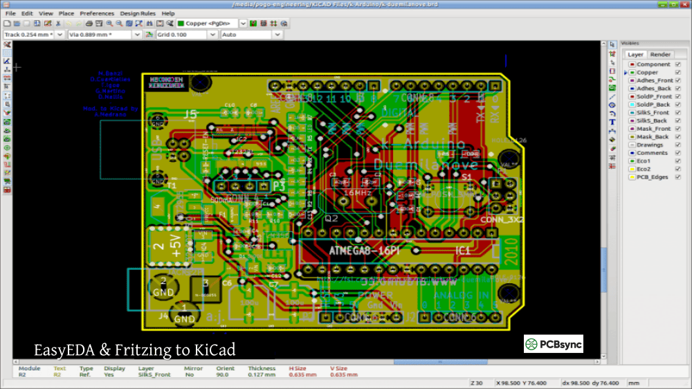
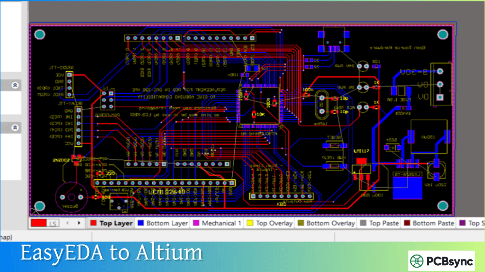
Yes, EasyEDA supports importing designs from other EDA tools. You can import Eagle schematic, PCB, and library files directly. KiCad files need to be compressed as a ZIP before importing. Altium Designer files must be saved in ASCII format first. The import isn’t always perfect—you may need to fix some details after conversion—but it provides a solid starting point for migrating existing projects.
What’s the difference between EasyEDA Standard and Pro editions?
Both editions are free. Standard Edition is ideal for learning, hobby projects, and straightforward professional work. It includes all essential features: schematic capture, simulation, PCB layout, and manufacturing file export. Pro Edition adds enterprise-focused capabilities like real-time team collaboration, modular design reuse blocks, enhanced BOM management, and support for very large designs (tens of thousands of components). Most individual users and small teams find Standard Edition perfectly sufficient.
Moving Forward with Your PCB Design Journey
You’ve now got a solid foundation in EasyEDA and PCB design fundamentals. The path forward involves practice, iteration, and gradual expansion of complexity.
Start with a simple project—a blinking LED circuit or a basic power supply. Complete the entire workflow from schematic through fabrication. Hold that first board you designed in your hands. That tangible result transforms abstract knowledge into real capability.
As you gain confidence, tackle progressively challenging designs. Add more components. Try surface-mount parts. Experiment with multi-layer boards. Each project teaches something new about design techniques, manufacturing constraints, and debugging strategies.
The EasyEDA free platform removes cost as a barrier to learning. Unlike expensive professional tools, you can experiment without financial pressure. Make mistakes, iterate quickly, and develop intuition through hands-on experience.
PCB design combines creativity with engineering discipline. There’s genuine satisfaction in transforming a circuit idea into a functional, professional-looking board. The Easy EDA tool makes that transformation accessible to anyone willing to learn—regardless of formal education or previous experience.
Your next great electronics project starts with a single schematic. Open www.easyeda.com, create that first component, draw that first wire, and begin the journey from idea to manufactured reality. The tools are free, the community is supportive, and the only limit is your imagination.
Inquire: Call 0086-755-23203480, or reach out via the form below/your sales contact to discuss our design, manufacturing, and assembly capabilities.
Quote: Email your PCB files to Sales@pcbsync.com (Preferred for large files) or submit online. We will contact you promptly. Please ensure your email is correct.
Notes: For PCB fabrication, we require PCB design file in Gerber RS-274X format (most preferred), *.PCB/DDB (Protel, inform your program version) format or *.BRD (Eagle) format. For PCB assembly, we require PCB design file in above mentioned format, drilling file and BOM. Click to download BOM template To avoid file missing, please include all files into one folder and compress it into .zip or .rar format.


