Inquire: Call 0086-755-23203480, or reach out via the form below/your sales contact to discuss our design, manufacturing, and assembly capabilities.
Quote: Email your PCB files to Sales@pcbsync.com (Preferred for large files) or submit online. We will contact you promptly. Please ensure your email is correct.
Notes: For PCB fabrication, we require PCB design file in Gerber RS-274X format (most preferred), *.PCB/DDB (Protel, inform your program version) format or *.BRD (Eagle) format. For PCB assembly, we require PCB design file in above mentioned format, drilling file and BOM. Click to download BOM template To avoid file missing, please include all files into one folder and compress it into .zip or .rar format.
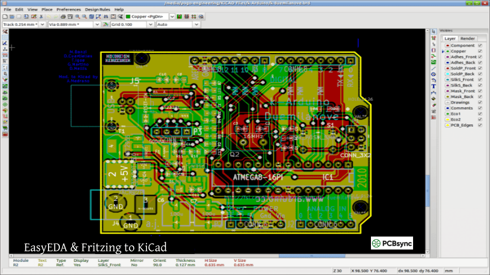
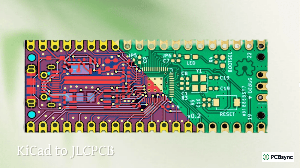
EasyEDA & Fritzing to KiCad: Migration Guide for Beginners
Starting your PCB design journey with beginner-friendly tools like EasyEDA or Fritzing makes perfect sense. These platforms offer gentle learning curves and quick results. But at some point, many hobbyists and makers hit a wall—maybe you need offline access, want more advanced features, or simply prefer owning your designs without cloud dependencies.
That’s when KiCad enters the picture. And if you’re sitting on a pile of EasyEDA or Fritzing projects wondering how to bring them into KiCad, you’re in the right place. I’ve helped dozens of makers navigate this transition, and I’ll walk you through every practical method for converting your designs.
Why Beginners Migrate from EasyEDA and Fritzing to KiCad
Before diving into the conversion process, understanding why so many hobbyists make this switch helps frame the effort involved.
EasyEDA works great for quick projects, especially when ordering from JLCPCB. The browser-based interface requires no installation, and the integration with LCSC component library simplifies parts selection. However, the cloud dependency means you need internet access, and some advanced features sit behind a paywall.
Fritzing excels at teaching electronics concepts. That breadboard view helps beginners visualize their circuits in a familiar way. But Fritzing wasn’t designed for complex professional work—it lacks advanced DRC, proper multi-sheet schematics, and sophisticated routing tools.
KiCad offers unlimited board complexity with no artificial restrictions. It runs entirely offline, your files stay on your computer, and the open-source community continuously improves the tool. Once you learn KiCad’s workflow, you’ll find it handles everything from simple Arduino shields to complex multi-layer boards.
Tool Comparison: Understanding What You’re Working With
Feature
EasyEDA
Fritzing
KiCad
Cost
Free (freemium)
Paid ($8)
Free, Open Source
Platform
Web-based
Windows, Mac, Linux
Windows, Mac, Linux
Offline Use
Limited
Full
Full
Learning Curve
Easy
Very Easy
Moderate
Max Layers
32
2
Unlimited
3D Viewer
Yes
No
Yes
Schematic Hierarchy
Basic
No
Full Support
JLCPCB Integration
Native
Via export
Via plugins
Community Size
Medium
Small
Large
Converting EasyEDA Projects to KiCad
The EasyEDA to KiCad conversion has become significantly easier thanks to community-developed tools. You have several options depending on whether you need just the PCB, just the libraries, or the complete project.
Method 1: Wokwi Online Converter for Quick PCB Conversion
This browser-based tool handles straightforward PCB conversions without any software installation. It processes your files locally in your browser, so nothing gets uploaded to external servers.
Step 1: Export from EasyEDA
In EasyEDA, open your project and navigate to Document → Export → EasyEDA Source. Save the JSON file to your computer.
Step 2: Convert Online
Visit wokwi.com/tools/easyeda2kicad and click to upload your EasyEDA board JSON file. The conversion happens automatically in your browser.
Step 3: Download and Open
The converter generates a .kicad_pcb file. Open this directly in KiCad’s PCB Editor to see your converted layout.
This method works best for simple boards when you only need the PCB layout. Schematics require different approaches.
Method 2: easyeda2kicad Python Tool for Component Libraries
When you want to leverage LCSC components in KiCad while maintaining proper symbols, footprints, and 3D models, the easyeda2kicad.py tool delivers excellent results.
Installation:
pip install easyeda2kicad
Converting a Single Component by LCSC ID:
easyeda2kicad –full –lcsc_id=C2040
This command downloads the component data from LCSC/EasyEDA and generates KiCad-compatible symbol, footprint, and 3D model files.
Batch Converting Multiple Components:
easyeda2kicad –full –lcsc_id=C2040,C14663,C25804
Setting Up the Library in KiCad:
After conversion, add the generated libraries to KiCad:
Go to Preferences → Manage Symbol Libraries
Click Add and browse to the generated .kicad_sym file
Go to Preferences → Manage Footprint Libraries
Click Add and browse to the generated .pretty folder
The converted libraries include 3D models in both WRL and STEP formats, which display properly in KiCad’s 3D viewer.
Method 3: easyeda2kicad6 for Complete Project Migration
For full project conversion including schematics and PCB with synchronized components, the easyeda2kicad6 TypeScript tool provides the most comprehensive solution.
Prerequisites:
Node.js installed on your system
Your EasyEDA project exported as JSON
Conversion Steps:
Export both schematic and PCB as JSON from EasyEDA
Run the converter on the PCB file first
Open the converted PCB in KiCad and export footprints to a library
Replace the PCB JSON with the schematic JSON (same filename)
Run the converter again for the schematic
Open both files in KiCad and sync them
Post-Conversion Checklist:
After importing, several manual steps ensure a clean project:
Task
Action in KiCad
Rebuild copper pours
Press B in PCB Editor
Run DRC
Inspect → Design Rules Checker
Run ERC
Inspect → Electrical Rules Checker
Verify footprint links
Tools → Edit Symbol Library Links
Check 3D models
View → 3D Viewer
Converting Fritzing Projects to KiCad
Fritzing to KiCad conversion presents more challenges because these tools have fundamentally different design philosophies. Fritzing focuses on visual breadboard representation, while KiCad follows traditional schematic-to-PCB workflow.
Understanding the Limitations
No automated tool provides perfect Fritzing to KiCad conversion for complete projects. The breadboard view in Fritzing has no equivalent in KiCad, and the schematic representation differs significantly.
Your realistic options include netlist export for routing reference, individual part conversion, and manual recreation using the Fritzing design as reference.
Method 1: XML Netlist Export and Conversion
Fritzing can export an XML netlist that captures your circuit connections. The xml2net Python tool converts this to a format KiCad can import.
Steps:
In Fritzing, go to File → Export → Netlist (XML)
Download xml2net from GitHub (github.com/KeithSloan/xml2net)
Run the conversion: python xml2net.py fritzing_netlist.xml
Import the resulting netlist into KiCad
This approach gives you the connection information but not the actual schematic or PCB layout. You’ll need to place components and route the board manually in KiCad.
Method 2: Fritzing2Kicad for Part Conversion
The Fritzing2Kicad tool converts individual Fritzing parts to KiCad symbols and footprints.
What It Converts:
Fritzing .fzpz part files
Schematic symbols
PCB footprints
What It Doesn’t Convert:
Complete projects
Breadboard views
Routing information
This tool helps when you have custom Fritzing parts you want to use in KiCad rather than redrawing them.
Method 3: Practical Manual Migration Workflow
For most Fritzing users, a systematic manual recreation produces better results than fighting with partial conversions.
Recommended Workflow:
Open your Fritzing project and switch to Schematic view
In KiCad, create a new project
Recreate the schematic component by component, using Fritzing as reference
Assign footprints in KiCad (often better quality than Fritzing equivalents)
Generate the PCB from schematic
Use Fritzing’s PCB view as placement reference while routing in KiCad
This approach takes more time initially but results in a clean, maintainable KiCad project without conversion artifacts.
Converting DipTrace Projects to KiCad
DipTrace users looking to migrate face a situation where direct import isn’t available, but workable paths exist.
Current DipTrace to KiCad Options
DipTrace can import KiCad files (version 7.x supported), but the reverse path requires intermediate steps or manual recreation.
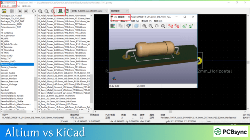
Option 1: Through Altium (if available)
If you have access to Altium Designer, you can import DipTrace files via PADS/PCAD format and then export to KiCad.
Option 2: Gerber Export
Export your DipTrace PCB as Gerber files. While KiCad can view Gerbers, this doesn’t provide an editable design. Use it as a reference for manual recreation.
Option 3: Manual Recreation
Many engineers who’ve made this switch report that recreating designs manually, while time-consuming, results in cleaner projects. DipTrace and KiCad share similar schematic-to-PCB workflows, making the learning curve manageable.
Converting OrCAD Designs to KiCad
OrCAD to KiCad migration requires more effort due to the proprietary .olb library format. However, several paths exist.
OrCAD Library Conversion Tools
Tool
Function
Link
orlib2ki
Converts OrCAD .olb libraries to KiCad
github.com/fjullien/orlib2ki
pyorlib2ki
Python-based OrCAD library converter
Available on PyPI
Conversion Process:
In OrCAD, export your libraries to XML format
Run the converter: orlib2ki -i myLibrary.xml
Import the resulting .lib file into KiCad
OrCAD Schematic Migration
OrCAD schematics don’t convert directly to KiCad. Your options include EDIF export (though KiCad’s EDIF support is limited), manual schematic recreation, and using Altium as an intermediary if available.
For PCB layouts, exporting as Gerber provides manufacturing files but not editable designs.
When components appear without footprints, the library paths aren’t configured correctly. Add the generated .pretty folder to your footprint libraries through Preferences → Manage Footprint Libraries.
Copper Pours Not Displaying
KiCad doesn’t store calculated zone fills. Press B in the PCB Editor to rebuild all copper pours. This is expected behavior, not an error.
DRC Errors on Fresh Import
Some DRC errors after conversion are normal. Review each error type—many result from format differences rather than actual design problems. Focus on clearance violations and unconnected nets first.
3D Models Missing or Flat
Converted designs often lack 3D model associations. Download models from component manufacturers or SnapMagic, then assign them in the footprint properties.
Frequently Asked Questions
Can I convert EasyEDA projects to KiCad without losing my routing?
Yes, the Wokwi online converter and easyeda2kicad6 tool preserve PCB routing. Copper pours need regeneration in KiCad (press B), but traces transfer correctly. Always verify with DRC after conversion.
Is there a direct Fritzing to KiCad converter?
No comprehensive converter exists for complete Fritzing projects. The fundamental design philosophies differ too much. Use xml2net for netlist transfer or Fritzing2Kicad for individual parts, but expect to recreate schematics and layouts manually for best results.
Will my JLCPCB part numbers work after converting from EasyEDA?
The easyeda2kicad.py tool specifically handles LCSC components (which JLCPCB uses). You can convert parts by LCSC ID, and the generated footprints maintain compatibility with JLCPCB assembly services.
How long does migration typically take for a beginner project?
A simple single-sheet schematic with 20-30 components typically converts in under an hour using automated tools. Manual cleanup and verification add another hour or two. Complex multi-sheet designs with custom parts may take a full day. Practice with a simple project first to establish your workflow.
Should I convert old projects or start fresh in KiCad?
For projects you’ll actively maintain or manufacture again, converting or recreating in KiCad makes sense. For archived designs you won’t modify, keep them in the original format and simply generate new Gerbers if needed. Most engineers leave legacy projects alone and start new work in KiCad.
Post-Migration Workflow Tips
After successfully converting your projects, establishing good KiCad habits prevents future headaches.
Organize Your Custom Libraries
Create a consistent folder structure for converted and custom libraries. Many engineers use something like:
This organization makes library management straightforward as your collection grows.
Verify Converted Footprints Before Manufacturing
Never send a board to fabrication without verifying critical footprints. Conversion tools sometimes produce incorrect pad sizes or positions. Print a 1:1 scale footprint check sheet and physically verify component fit before ordering PCBs.
Build a Verification Checklist
Check
How to Verify
Pad sizes match datasheet
Measure in footprint editor
Pin 1 marking correct
Compare to component datasheet
Courtyard appropriate
Visual check in 3D viewer
Hole sizes correct
Check drill file output
Silkscreen readable
Generate fabrication output
Understanding File Format Differences
Knowing what happens during conversion helps troubleshoot issues.
EasyEDA File Structure
EasyEDA uses JSON format for both schematics and PCBs. This text-based format makes parsing relatively straightforward, which is why multiple conversion tools exist. The JSON includes component placements, connections, and routing data in a structured but proprietary schema.
Fritzing File Structure
Fritzing uses .fzz files (renamed ZIP archives) containing SVG graphics and XML data. The breadboard view complexity and SVG-based part definitions make automated conversion challenging. Each view (breadboard, schematic, PCB) stores data separately, and connections rely on visual SVG overlays.
KiCad File Structure
KiCad uses S-expression format (.kicad_sch, .kicad_pcb) that’s human-readable and well-documented. This openness benefits the conversion ecosystem—developers can create tools without reverse-engineering proprietary formats.
Making the Transition Smoother
Moving from Easy EDA to KiCad or Fritzing to KiCad represents a real learning investment. Here’s how to make it manageable:
Start with a simple project you understand well. Converting something complex while simultaneously learning KiCad’s interface leads to frustration. Pick a design with maybe 10-15 components and a single-layer or two-layer board.
Learn KiCad basics before attempting conversion. Spend a few hours following a beginner tutorial to understand the schematic-to-PCB workflow. This context helps when troubleshooting conversion issues.
Keep your original files. Never overwrite or delete your EasyEDA or Fritzing projects. Conversion isn’t always perfect, and you may need to reference the original or extract specific elements later.
Join the KiCad community. The forum at forum.kicad.info has incredibly helpful members who’ve seen every migration scenario imaginable. Search existing threads before posting—chances are someone has solved your specific problem.
Whether you’re moving from KiCad EasyEDA workflows to pure KiCad, transitioning from KiCad Fritzing hybrid approaches, or migrating from DipTrace to KiCad or OrCAD to KiCad, the destination is worth the journey. KiCad’s capabilities grow with you from hobbyist projects through professional-grade designs, and your converted projects become truly yours—files you control on hardware you own.
Inquire: Call 0086-755-23203480, or reach out via the form below/your sales contact to discuss our design, manufacturing, and assembly capabilities.
Quote: Email your PCB files to Sales@pcbsync.com (Preferred for large files) or submit online. We will contact you promptly. Please ensure your email is correct.
Notes: For PCB fabrication, we require PCB design file in Gerber RS-274X format (most preferred), *.PCB/DDB (Protel, inform your program version) format or *.BRD (Eagle) format. For PCB assembly, we require PCB design file in above mentioned format, drilling file and BOM. Click to download BOM template To avoid file missing, please include all files into one folder and compress it into .zip or .rar format.


