Inquire: Call 0086-755-23203480, or reach out via the form below/your sales contact to discuss our design, manufacturing, and assembly capabilities.
Quote: Email your PCB files to Sales@pcbsync.com (Preferred for large files) or submit online. We will contact you promptly. Please ensure your email is correct.
Notes: For PCB fabrication, we require PCB design file in Gerber RS-274X format (most preferred), *.PCB/DDB (Protel, inform your program version) format or *.BRD (Eagle) format. For PCB assembly, we require PCB design file in above mentioned format, drilling file and BOM. Click to download BOM template To avoid file missing, please include all files into one folder and compress it into .zip or .rar format.
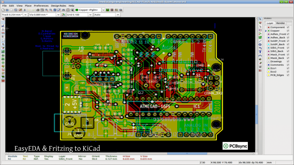
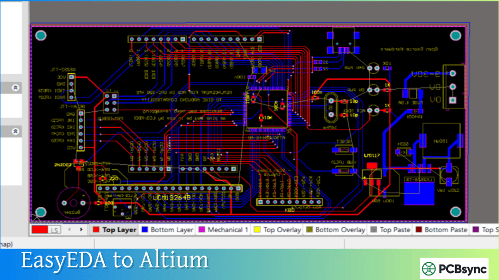
EasyEDA Autoroute, DRC & Net Management: The Complete Guide to Fixing Unfinished Nets and Ratlines
If you’ve spent any time routing PCBs in EasyEDA, you’ve probably encountered that frustrating “Incomplete Connection, please check” message. Those stubborn ratlines that refuse to disappear, even when everything looks connected, can turn a simple project into hours of troubleshooting.
I’ve been designing PCBs professionally for over eight years, and I still remember the first time I watched the EasyEDA autorouter hit 85% completion and just… stop. No error message explaining what went wrong. Just a half-finished board and a lot of confusion.
This guide pulls together everything I’ve learned about EasyEDA autoroute, DRC settings, and net management. Whether you’re trying to understand why your autorouter keeps failing or hunting down that one unfinished net hiding in your design, you’ll find practical solutions here.
Understanding EasyEDA Autoroute: How the Built-in Router Actually Works
The EasyEDA autoroute function lives under Route > Auto Router in the top menu. Before clicking that button, though, it helps to understand what the autorouter can and cannot do.
How EasyEDA Autoroute Processes Your Design
The built-in autorouter works by analyzing your ratlines and attempting to create copper traces that connect all the pads belonging to each net. It operates according to a set of priorities and rules you can configure.
It sorts nets according to your selected priority (more on this below)
For each net, it attempts to find a valid routing path
If blocked, it tries alternative paths or layer changes
The process continues until complete or the time limit expires
EasyEDA Autoroute Configuration Options
When you open the autorouter dialog, you’ll see several important settings:
Setting
Options
Recommendation
Routing Corner
45° or 90°
Use 45° for production boards
Existing Tracks/Vias
Keep or Remove
Keep if you’ve pre-routed critical traces
Effect Priority
Speed or Completion
Choose Completion for thorough routing
Net Priority
Multiple options
Use “Pads Farthest to Nearest” for complex boards
Router Server
Cloud or Local
Local is more reliable under heavy load
Net Priority Settings Explained
The net priority setting significantly impacts your routing success rate. Here’s what each option actually does:
Default routes nets in the order the editor reads them. This is essentially random and rarely optimal.
Pads from Most to Least prioritizes complex nets with many connections. This can help route difficult nets before the board gets congested.
Pads Farthest to Nearest sorts by the total distance between pads in each net. Starting with nets that span the board helps establish main routing channels early.
User-defined Network Name Priority puts nets without $ prefixes first, sorted alphabetically. This gives you direct control over routing order.
EasyEDA DRC Settings: Configuring Design Rules Before You Route
Running the EasyEDA autoroute without proper DRC settings is like driving without looking at the road. Your autorouter uses these rules to determine what’s allowed during routing.
Accessing EasyEDA DRC Settings
Open the Design Rule dialog through Tools > Design Rule or right-click the canvas and select Design Rule. The unit displayed matches your canvas unit setting.
Essential EasyEDA DRC Parameters
Parameter
What It Controls
Typical Value
Track Width
Minimum trace width
6-10 mil for signal traces
Clearance
Spacing between different nets
6-8 mil minimum
Via Diameter
Outer diameter of vias
24-30 mil
Via Drill Diameter
Hole size for vias
12-16 mil
Track Length
Maximum trace length per net
Leave empty unless length-matching
Real-time DRC: Your First Line of Defense
Enable Realtime DRC in the Design Rule dialog. When active, EasyEDA displays an X mark wherever a DRC violation occurs during routing. This immediate feedback prevents errors from accumulating.
The real-time DRC checks:
Track to track spacing
Track to pad clearance
Via placement violations
Board outline proximity
Setting Up Multiple Design Rules
EasyEDA allows creating custom rules for specific nets. This is essential when your board has mixed requirements, like power traces needing wider widths than signal traces.
To create a custom rule:
Open Design Rule dialog
Click the + icon next to the default rule
Name your new rule (e.g., “PowerNets”)
Set the parameters
Assign nets to this rule in the Design Manager
Common EasyEDA DRC Error Types
When you run a DRC check via Design > Check DRC or the Design Manager, you might encounter these errors:
Clearance Error: Two objects from different nets are too close. The DRC reports the actual spacing versus the required clearance.
Track Width Error: A trace is narrower than the minimum specified in Design Rules.
Via Diameter Error: Via is smaller than the minimum allowed.
Incomplete Connection: Parts of a net aren’t connected by copper. This is where ratlines come into play.
Understanding EasyEDA Nets and the Design Manager
Nets form the backbone of your PCB design. Every connection shown in your schematic creates a net that the PCB editor must route.
How EasyEDA Nets Work
A net in EasyEDA is defined by:
A unique name (either user-assigned or auto-generated)
Two or more pads that should be electrically connected
Ratlines showing the required connections
The Design Manager, found in the left panel, displays all nets in your design. Click a net name to highlight it on the canvas. A check mark indicates the net is fully routed; missing check marks show incomplete routing.
Net Classes for Organized Design
EasyEDA Pro supports net classes, which group related nets together. Access this through Design > Network Class Manager.
Use net classes to:
Apply design rules to groups of nets
Skip certain nets during autorouting (like GND for copper pours)
Organize complex designs with hundreds of nets
Viewing Net Information
Several methods help you inspect net properties:
Design Manager Panel: Shows all nets, their routing status, and allows visibility toggling.
Net Highlighting: Click any track and press H to highlight the entire net. A popup shows the total net length.
Net Colors: Right-click a net in Design Manager or go to Tools > Net Color to assign distinctive colors for easier tracking.
EasyEDA Ratlines: What They Mean and How to Manage Them
Ratlines are the thin connection lines showing where copper traces need to go. When a ratline remains visible after routing, you have an EasyEDA unfinished net.
Why Ratlines Persist After Autorouting
Several reasons explain persistent ratlines:
The autorouter couldn’t find a valid path. This happens when clearance requirements block all possible routes.
Time limit expired. The “Speed Priority” setting stops routing after a timeout, leaving some nets incomplete.
Net naming conflicts. Special characters in net names can confuse the autorouter.
Copper pour connections. Nets intended for connection via copper area still show ratlines until the pour is rebuilt.
Managing Ratline Visibility
Sometimes you need to hide ratlines temporarily to focus on specific routing:
Open Design Manager
Uncheck the net you want to hide (e.g., GND before adding copper pour)
The ratline disappears but the net remains in your design
To see all ratlines clearly:
Go to Layer Manager
Click the pencil icon next to Ratlines
Change the color to something highly visible like bright red
The Ratline Visibility Trick for Finding Incomplete Nets
When you have hundreds of nets, finding the few incomplete ones takes time. Here’s what I do:
In Layer Manager, hide all layers except Ratlines
Toggle Ratlines visibility off and on
Watch for the ratlines that flash during the toggle
These are your incomplete nets
In newer EasyEDA versions, incomplete nets automatically sort to the top of the Design Manager list.
Now for the part everyone searches for: actually fixing those stubborn unfinished nets.
Step-by-Step Troubleshooting Process
Step 1: Verify Schematic Connections
Before blaming the PCB editor, check your schematic:
Use the Wire tool (W hotkey), not the Line tool from Drawing Tools
Ensure red solder dots appear at wire junctions
Click “Check Design” in Design Manager to find floating pins
Step 2: Check Net Names
Open Design Manager and look for:
Duplicate net names with slightly different suffixes
Nets with special characters (parentheses, brackets)
Unintended net splits from incorrect labeling
EasyEDA is case-insensitive, so “MyNet” equals “mynet”. Use only alphanumeric characters and underscores in net names.
Step 3: Rebuild Copper Pours
If your unfinished nets involve GND or power planes:
Select the copper area
Press Shift+B to rebuild
Check if ratlines disappear
Sometimes copper areas don’t connect properly due to thermal relief settings or isolation gaps.
Step 4: Examine Physical Routing
For nets that show connected but still display ratlines:
Zoom in on connection points
Verify tracks actually touch pads
Check that vias connect to the correct layers
Common Unfinished Net Causes and Fixes
Problem
Symptoms
Solution
Pad not connected to track
Ratline shows, track appears connected
Zoom in, delete track, re-route directly to pad center
Wrong layer via
Net incomplete on inner layers
Check via spans correct layers
Copper pour not rebuilt
GND ratlines persist
Shift+B to rebuild all copper areas
Footprint pin mismatch
Schematic pin doesn’t match PCB pad
Edit footprint, match pin numbers
Grid snap misalignment
Objects not quite touching
Enable snap, adjust grid settings
Net name special characters
Autorouter skips nets
Rename nets using only A-Z, 0-9, underscore
Manual Routing Techniques for Stubborn Nets
When autorouting fails repeatedly, manual routing becomes necessary:
RoundTrack Mode: In the Properties panel, set Routing Conflict to “RoundTrack”. Traces automatically walk around obstacles.
Layer Switching: During manual routing, press V to add a via and switch layers. Press L to change the corner angle.
Track Segment Deletion: To remove part of a track without deleting the whole thing, click the segment, hold Shift, and double-click to delete just that segment.
Using EasyEDA Mil to MM Conversion for Precise Design
PCB design uses both imperial (mil) and metric (mm) units. EasyEDA supports both, but switching between them requires care.
Changing Units in EasyEDA
Quick Method: Press Q to toggle between mil and mm.
Properties Method:
Open the right Properties panel
Under Canvas Attributes, find Units
Select mm or mil from the dropdown
The unit setting also affects DRC values, so verify your Design Rules after switching.
EasyEDA Mil to MM Conversion Reference
Mils
Millimeters
Common Use
6 mil
0.1524 mm
Fine pitch clearance
8 mil
0.2032 mm
Standard clearance
10 mil
0.254 mm
Signal trace width
12 mil
0.3048 mm
Narrow power trace
24 mil
0.6096 mm
Standard via diameter
40 mil
1.016 mm
Wide power trace
100 mil
2.54 mm
Standard header pitch
Remember: 1 mil = 0.0254 mm, or 1 mm = 39.37 mils
Avoiding Unit Conversion Problems
A common issue occurs when switching units mid-design. EasyEDA recalculates values, and rounding errors can trigger false DRC violations.
Example: You set via diameter to 24 mil, switch to mm (0.6096mm), then back to mil. The via might now show as 23.999 mil, triggering a “Via Diameter” DRC error.
Best Practice: Choose your unit system at project start and stick with it. If your fab uses mm specifications, design in mm.
Using Third-Party Autorouters with EasyEDA
When the built-in EasyEDA autoroute struggles, third-party tools can help. EasyEDA supports DSN/SES file exchange with external autorouters.
Freerouting: The Best Free Alternative
Freerouting is an open-source autorouter that often outperforms EasyEDA’s built-in option on complex boards.
FAQs About EasyEDA Autoroute, DRC, and Net Management
Why does my EasyEDA autoroute stop at 85-95% completion?
The autorouter stops when it cannot find valid paths for remaining nets. This usually means your component placement creates routing bottlenecks. Try these fixes:
Spread components farther apart
Reduce clearance settings (within fab capabilities)
Route critical nets manually first, then autoroute the rest
Use Freerouting as an alternative autorouter
How do I fix “Incomplete Connection” errors in EasyEDA?
First, identify which nets are incomplete using Design Manager. Then check:
Schematic connections use Wire tool, not Line tool
Net labels have consistent naming (no special characters)
Footprint pad numbers match schematic pin numbers
Copper pours are rebuilt (Shift+B)
Tracks actually terminate on pads, not just near them
Can I change EasyEDA from mil to mm permanently?
You can change units per session through the Properties panel (Canvas Attributes > Units), but EasyEDA defaults to mil when starting new projects. There’s no permanent default setting, so you’ll need to change it each time or establish a project template.
Why do ratlines still show after I’ve routed all traces?
Ratlines indicate unconnected portions of a net. If traces appear routed but ratlines persist:
Zoom to 500%+ and verify physical connections
Check via layer spans match your intended routing layers
Rebuild copper pours with Shift+B
Look for tiny gaps caused by grid snap issues
How do I make EasyEDA autoroute use thicker traces for power nets?
Set up special net rules in Design Rules:
Create a new rule with wider track width (e.g., 24 mil)
In the autorouter dialog, use “Special Nets” section
Add your power net names and assign them the wider track rule
Run autoroute normally; it will use the special rules for designated nets
Wrapping Up
Getting clean autoroute results in EasyEDA comes down to three things: proper DRC configuration, good component placement, and understanding how nets work. The built-in autorouter won’t solve every routing problem, but combined with manual routing skills and tools like Freerouting, you can tackle boards of considerable complexity.
Start with tight DRC rules matching your fab’s capabilities. Place components to minimize crossing ratlines. Route critical nets manually before letting the autorouter handle the rest. And when those stubborn unfinished nets appear, work through the troubleshooting steps systematically.
The time you spend learning EasyEDA’s net management and DRC features pays dividends on every future project. A board that passes DRC on the first check is a board that comes back from the fab working as designed.
Inquire: Call 0086-755-23203480, or reach out via the form below/your sales contact to discuss our design, manufacturing, and assembly capabilities.
Quote: Email your PCB files to Sales@pcbsync.com (Preferred for large files) or submit online. We will contact you promptly. Please ensure your email is correct.
Notes: For PCB fabrication, we require PCB design file in Gerber RS-274X format (most preferred), *.PCB/DDB (Protel, inform your program version) format or *.BRD (Eagle) format. For PCB assembly, we require PCB design file in above mentioned format, drilling file and BOM. Click to download BOM template To avoid file missing, please include all files into one folder and compress it into .zip or .rar format.


