Inquire: Call 0086-755-23203480, or reach out via the form below/your sales contact to discuss our design, manufacturing, and assembly capabilities.
Quote: Email your PCB files to Sales@pcbsync.com (Preferred for large files) or submit online. We will contact you promptly. Please ensure your email is correct.
Notes: For PCB fabrication, we require PCB design file in Gerber RS-274X format (most preferred), *.PCB/DDB (Protel, inform your program version) format or *.BRD (Eagle) format. For PCB assembly, we require PCB design file in above mentioned format, drilling file and BOM. Click to download BOM template To avoid file missing, please include all files into one folder and compress it into .zip or .rar format.
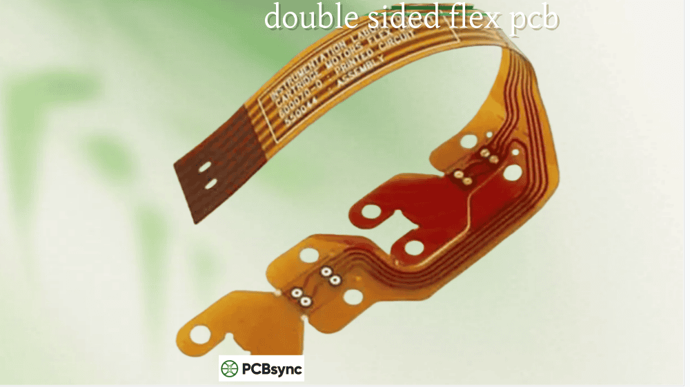
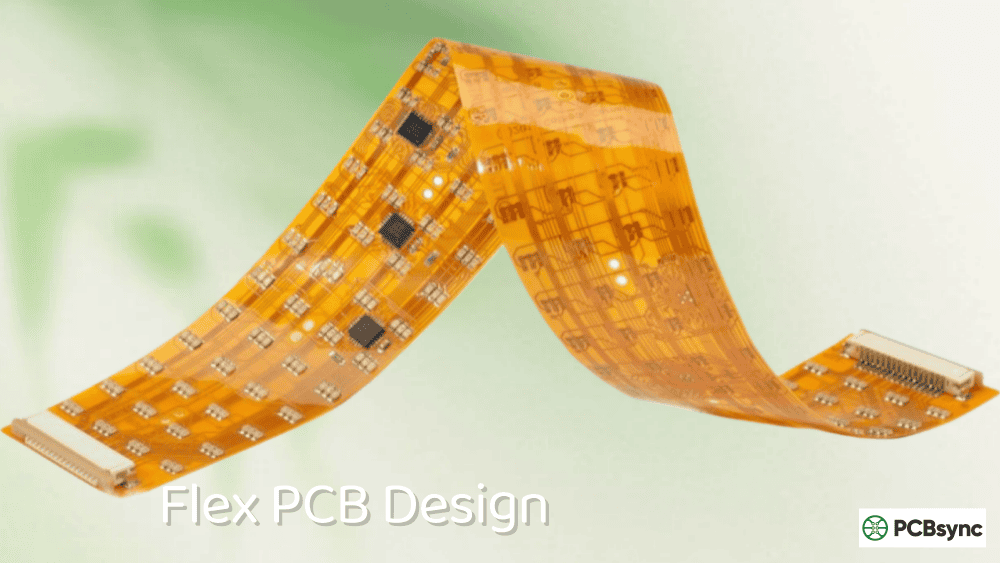
Double Sided Flex PCB: Structure, Manufacturing Process & Use Cases
When I first moved from rigid board design to flexible circuits about twelve years ago, the jump to double sided flex PCB felt like unlocking a new dimension. Single-layer flex was straightforward—essentially a flexible wire with patterned traces. But adding that second conductive layer changed everything. Suddenly I could route signal crossovers, integrate ground planes, and pack twice the circuit density into the same footprint. The learning curve was steep, but the design possibilities made it worthwhile.
If you’re evaluating whether double sided flex PCB makes sense for your project, or if you’re already committed and need to understand the manufacturing nuances, this guide covers the essential structure, fabrication process, and real-world applications where two-layer flex circuits excel.
A double sided flex PCB is a flexible printed circuit board featuring two conductive copper layers separated by a flexible dielectric substrate, typically polyimide. Unlike single-layer flex circuits where traces exist on only one side, double-sided designs allow circuit patterns on both top and bottom surfaces, connected through plated through-holes (PTHs) or vias.
This configuration increases routing density without expanding the circuit footprint—a critical advantage when space constraints drive design decisions. The two copper layers enable signal crossovers without jumper wires, dedicated ground or power planes for improved signal integrity, and component mounting on both sides of the circuit.
Double sided flex PCB retains the fundamental benefits of flexible circuits: the ability to bend, fold, and conform to three-dimensional shapes while maintaining electrical connectivity. However, the added layer complexity introduces manufacturing considerations and slightly reduces flexibility compared to single-layer designs.
Structure and Stack-Up of Double Sided Flex PCB
Understanding the layer construction is essential for specifying materials correctly and working effectively with your fabricator.
Standard Double Sided Flex PCB Stack-Up
Layer Position
Material
Typical Thickness
Function
Top Coverlay
Polyimide + adhesive
25-50 μm
Protects top copper traces
Top Copper
RA or ED copper
9-35 μm (¼-1 oz)
Top signal/power layer
Adhesive
Acrylic or epoxy
12.5-25 μm
Bonds copper to core (adhesive-based)
Core Dielectric
Polyimide (PI)
12.5-50 μm
Flexible insulating substrate
Adhesive
Acrylic or epoxy
12.5-25 μm
Bonds copper to core (adhesive-based)
Bottom Copper
RA or ED copper
9-35 μm (¼-1 oz)
Bottom signal/power layer
Bottom Coverlay
Polyimide + adhesive
25-50 μm
Protects bottom copper traces
Total thickness for a typical double sided flex PCB ranges from 0.1mm to 0.26mm, depending on copper weight and material selections.
Adhesive vs Adhesiveless Construction
Double sided flex PCB can be manufactured using two fundamentally different approaches:
Adhesive-based construction bonds copper foils to the polyimide core using thin adhesive layers (typically acrylic or epoxy). This is the more common and cost-effective approach, suitable for most applications.
Adhesiveless construction deposits or laminates copper directly onto the polyimide without intermediate adhesive. This produces thinner circuits with improved flexibility and better high-temperature performance. Adhesiveless flex costs more but excels in dynamic flexing applications and designs requiring tight bend radii.
Material Options for Double Sided Flex
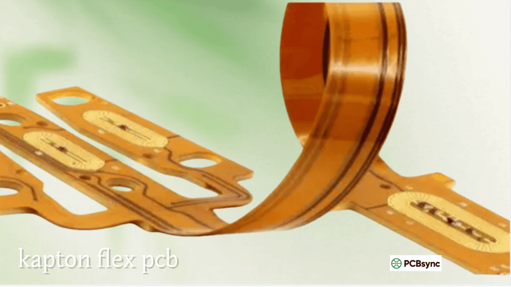
Polyimide (PI) remains the dominant substrate material for double sided flex PCB. Kapton and similar polyimides offer excellent thermal stability (withstanding 260°C+ soldering temperatures), chemical resistance, and mechanical durability across millions of flex cycles.
Polyester (PET) provides a lower-cost alternative for static flex applications where temperature requirements are modest (below 105°C). PET isn’t suitable for soldering processes, so component attachment requires alternative methods.
LCP (Liquid Crystal Polymer) offers superior electrical properties for high-frequency applications, with lower moisture absorption and more stable dielectric constant than polyimide.
Copper Types: Choosing Between RA and ED
Rolled Annealed (RA) copper is essential for dynamic flexing applications. The rolling process aligns the copper grain structure, dramatically improving fatigue resistance. RA copper can withstand millions of flex cycles without cracking—critical for applications like printer heads, disk drive connections, and laptop hinges.
Electrodeposited (ED) copper costs less and works well for static or flex-to-install applications where the circuit bends once during assembly and remains stationary thereafter. ED copper’s perpendicular grain structure makes it more prone to fatigue cracking under repeated flexing.
Manufacturing Process for Double Sided Flex PCB
The fabrication process for double sided flex PCB shares many steps with rigid PCB manufacturing but requires specialized handling due to the flexible substrate. Understanding these steps helps you design for manufacturability and set realistic expectations for cost and lead time.
Step-by-Step Manufacturing Process
Step 1: Material Preparation Manufacturing begins with flexible copper-clad laminate (FCCL)—polyimide film pre-bonded to copper foil on both sides. The material arrives in rolls or sheets and is cut to panel size for processing.
Step 2: Drilling CNC drilling machines create through-holes for vias and component leads. Unlike rigid boards, flexible substrates require specialized fixturing to prevent movement during drilling. Laser drilling may be used for microvias in high-density designs.
Step 3: Hole Plating (PTH) Drilled holes are plated with copper to create electrical connections between the two conductive layers. Vertical continuous plating (VCP) technology ensures uniform copper thickness on via walls—critical for reliable double sided flex PCB performance.
Step 4: Dry Film Lamination Photosensitive dry film resist is laminated onto both copper surfaces. This film will define the circuit pattern during imaging.
Step 5: Exposure and Imaging UV light exposes the circuit pattern onto the photoresist using photo-tools (films) with the trace artwork. Exposed areas polymerize while unexposed areas remain soluble.
Step 6: Development Chemical development removes unexposed photoresist, revealing the copper to be etched away.
Step 7: Etching Etchant solution (typically cupric chloride or ammoniacal etchant) removes unwanted copper, leaving only the designed circuit pattern. The cured photoresist protects traces during etching.
Step 8: Resist Stripping Remaining photoresist is stripped away, leaving bare copper traces on both sides of the flexible substrate.
Step 9: Coverlay Lamination Pre-cut polyimide coverlay films are aligned and laminated over the etched circuits under heat and pressure. The coverlay functions like solder mask, protecting copper traces while leaving pads exposed for soldering.
Step 10: Surface Finish Exposed copper pads receive surface finish (ENIG, immersion tin, OSP, or other finishes) to protect against oxidation and ensure solderability.
Step 11: Electrical Testing Flying probe or fixture-based testing verifies continuity and isolation across the circuit. Every double sided flex PCB should pass electrical testing before shipment.
Step 12: Profiling and Singulation Individual circuits are cut from the panel using routing, laser cutting, or die punching, depending on volume and geometry.
Step 13: Stiffener Attachment (if required) FR4, polyimide, or metal stiffeners are bonded to designated areas requiring rigidity for component mounting or connector interfaces.
Step 14: Final Inspection and Packaging Visual inspection, dimensional verification, and final quality checks precede careful packaging to prevent damage during shipping.
Manufacturing Challenges Specific to Double Sided Flex
Double sided flex PCB offers significant benefits compared to both single-layer flex and rigid alternatives:
Increased Circuit Density
With traces on both surfaces, double sided flex PCB accommodates more complex routing without expanding the circuit footprint. Signal crossovers that would require jumper wires on single-layer flex happen naturally through the two-layer structure.
Enhanced Signal Integrity
Dedicated ground or power planes on one layer improve signal integrity by reducing crosstalk and providing controlled impedance paths. This capability is essential for high-speed digital and RF applications.
Component Mounting Flexibility
Components can mount on either or both sides of the circuit, maximizing space utilization in compact designs. This dual-side access enables higher component density than single-layer alternatives.
Design Versatility
The two-layer structure supports more complex circuit topologies while maintaining flexibility. Designers gain routing freedom comparable to rigid two-layer boards with the mechanical benefits of flex circuits.
Dynamic Flexing Capability
When designed with appropriate materials and bend radii, double sided flex PCB withstands continuous flexing during operation—essential for applications like disk drive actuators, robotic joints, and folding displays.
Double Sided Flex PCB vs Single Layer and Multilayer
Characteristic
Single Layer Flex
Double Sided Flex PCB
Multilayer Flex
Copper Layers
1
2
3 or more
Typical Thickness
0.08-0.15mm
0.1-0.26mm
0.2-0.5mm
Circuit Complexity
Simple
Moderate
High
Routing Density
Low
Medium
High
Signal Crossovers
Not possible
Yes, via layer change
Yes, multiple options
Ground Planes
Not possible
Yes, one layer
Yes, dedicated layers
Flexibility
Highest
Good
Reduced
Cost
Lowest
Moderate
Highest
Lead Time
Shortest
Moderate
Longest
Dynamic Flex Cycles
>500 million
>100 million
>10 million
Double sided flex PCB occupies the middle ground—offering substantially more capability than single-layer at a cost and complexity level well below multilayer designs. For many applications, it’s the optimal balance point.
Use Cases and Applications for Double Sided Flex PCB
Double sided flex PCB serves diverse industries where the combination of routing density, flexibility, and reliability matters:
Consumer Electronics
Smartphones, tablets, and laptops rely heavily on double sided flex PCB for internal connections. Camera modules, display interfaces, and battery connections commonly use two-layer flex for space-efficient routing with adequate signal integrity.
Specific applications:
Smartphone camera module connections
Laptop display hinge interconnects
Tablet touch screen interfaces
Wearable device internal wiring
Wireless earbuds battery and audio connections
Automotive Electronics
Modern vehicles contain hundreds of electronic subsystems, many utilizing double sided flex PCB for reliable connections in demanding environments with temperature extremes, vibration, and extended service life requirements.
Specific applications:
Dashboard display interfaces
Steering wheel controls
Seat position sensors and heaters
LED lighting interconnects
ADAS camera and sensor connections
Battery management systems in EVs
Medical Devices
Medical applications demand reliability, biocompatibility, and miniaturization—qualities where double sided flex PCB excels. The ability to conform to body contours while maintaining complex circuitry makes flex circuits essential for implantables and wearables.
Specific applications:
Hearing aid internal circuits
Glucose monitoring patches
Cardiac rhythm management devices
Endoscope camera modules
Patient monitoring sensors
Implantable neurostimulators
Industrial and Automation
Industrial control systems benefit from double sided flex PCB’s vibration resistance and ability to route through articulated machinery without the failure modes common to wire harnesses.
Specific applications:
Robotic arm joint connections
Printer head assemblies
Industrial sensor arrays
CNC machine interconnects
Barcode scanner optics
Aerospace and Defense
Weight reduction drives aerospace adoption of flex circuits, while reliability requirements demand the enhanced signal integrity that double sided flex PCB provides over single-layer alternatives.
Successful double sided flex PCB designs require attention to flex-specific guidelines beyond standard rigid board practices:
Trace Routing Guidelines
Parameter
Recommended Specification
Minimum Trace Width
4 mils (0.1mm), 6 mils preferred
Minimum Spacing
4 mils (0.1mm)
Trace Direction in Bend Areas
Perpendicular to bend line
Via Placement
Minimum 50 mils from bend zones
Annular Ring
≥8 mils for PTH reliability
Stagger Traces Between Layers
Avoid stacking traces through flex zones
Bend Radius Considerations
The minimum bend radius for double sided flex PCB is larger than single-layer due to increased thickness:
Static applications: Minimum bend radius = 6× total thickness
Dynamic applications: Minimum bend radius = 12-20× total thickness
For a 0.2mm thick double sided flex PCB, this means:
Static: 1.2mm minimum bend radius
Dynamic: 2.4-4.0mm minimum bend radius
Stiffener Application
Add stiffeners where components mount or connectors interface. Common stiffener materials include FR4 (cost-effective), polyimide (matched thermal expansion), and stainless steel or aluminum (heat dissipation).
Frequently Asked Questions About Double Sided Flex PCB
How much does double sided flex PCB cost compared to single layer?
Double sided flex PCB typically costs 30-50% more than equivalent single-layer designs. The premium reflects additional material (second copper layer, more complex FCCL), added processing steps (drilling, plating through-holes), and tighter manufacturing tolerances. For prototype quantities, expect $50-150 per design for single-layer versus $70-220 for double-sided. Production volumes see similar percentage differentials but lower absolute costs.
Can double sided flex PCB handle dynamic flexing applications?
Yes, when properly designed and manufactured. Use rolled annealed (RA) copper, adhesiveless construction if possible, maintain generous bend radii (12-20× thickness), route traces perpendicular to bend lines, and avoid placing vias in flex zones. Well-designed double sided flex PCB withstands 100 million+ flex cycles. For extreme dynamic requirements exceeding 500 million cycles, single-layer flex may be more appropriate.
What surface finishes work best for double sided flex PCB?
ENIG (Electroless Nickel Immersion Gold) is the most common finish for double sided flex PCB, providing excellent solderability, corrosion resistance, and flat surfaces for fine-pitch components. Immersion tin offers a lower-cost alternative for less demanding applications. OSP (Organic Solderability Preservative) works for immediate assembly but has limited shelf life. Hard gold plating is specified for contact fingers or edge connectors subject to repeated insertion.
How do I choose between double sided flex and rigid-flex PCB?
Double sided flex PCB is appropriate when you need a continuously flexible circuit connecting two or more points. Rigid-flex combines rigid board sections (where components mount) with flexible interconnects, eliminating connectors between rigid and flex portions. Choose rigid-flex when your design requires significant component mounting on rigid substrates with flexible interconnects between them. For simpler applications where components can mount on stiffened flex areas, double sided flex PCB is more cost-effective.
What’s the typical lead time for double sided flex PCB?
Standard prototype lead times run 7-10 days for double sided flex PCB, compared to 5-7 days for single-layer flex. Production quantities typically require 14-21 days. Quick-turn services from some manufacturers can deliver prototypes in 3-5 days at premium pricing. Factors affecting lead time include complexity, material availability, stiffener requirements, and surface finish selection.
Useful Resources for Double Sided Flex PCB Design
Design Standards
IPC-6013: Qualification and Performance Specification for Flexible/Rigid-Flexible Printed Boards
IPC-2223: Sectional Design Standard for Flexible Printed Boards
Making Your Decision: Is Double Sided Flex PCB Right for Your Project?
Double sided flex PCB makes sense when:
Your routing complexity exceeds single-layer capabilities
Signal integrity requires a ground or power plane
Component density demands dual-side mounting
The application requires flexibility with moderate circuit complexity
Cost constraints preclude multilayer flex
Stick with single-layer flex when:
Simple point-to-point connections suffice
Maximum flexibility is the priority
Budget is highly constrained
Lead time is critical
Consider multilayer flex when:
Routing complexity demands three or more signal layers
High-speed or controlled impedance requirements are paramount
Design density exceeds double-sided capabilities
For the majority of flexible circuit applications requiring more than basic connectivity, double sided flex PCB delivers the optimal combination of capability, flexibility, and cost-effectiveness. It’s the workhorse of the flex circuit world—not as simple as single-layer, not as complex as multilayer, but right where most real-world designs need to be.
That first double-sided flex project I mentioned taught me that the extra layer isn’t just about adding routing channels. It fundamentally changes what’s possible in a flexible circuit design. Once you’ve worked with two-layer flex, you’ll find applications for it everywhere.
Inquire: Call 0086-755-23203480, or reach out via the form below/your sales contact to discuss our design, manufacturing, and assembly capabilities.
Quote: Email your PCB files to Sales@pcbsync.com (Preferred for large files) or submit online. We will contact you promptly. Please ensure your email is correct.
Notes: For PCB fabrication, we require PCB design file in Gerber RS-274X format (most preferred), *.PCB/DDB (Protel, inform your program version) format or *.BRD (Eagle) format. For PCB assembly, we require PCB design file in above mentioned format, drilling file and BOM. Click to download BOM template To avoid file missing, please include all files into one folder and compress it into .zip or .rar format.


