Inquire: Call 0086-755-23203480, or reach out via the form below/your sales contact to discuss our design, manufacturing, and assembly capabilities.
Quote: Email your PCB files to Sales@pcbsync.com (Preferred for large files) or submit online. We will contact you promptly. Please ensure your email is correct.
Notes: For PCB fabrication, we require PCB design file in Gerber RS-274X format (most preferred), *.PCB/DDB (Protel, inform your program version) format or *.BRD (Eagle) format. For PCB assembly, we require PCB design file in above mentioned format, drilling file and BOM. Click to download BOM template To avoid file missing, please include all files into one folder and compress it into .zip or .rar format.
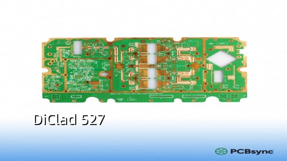
If you’ve spent any time designing high-frequency circuits, you know that material selection can make or break your project. I’ve worked with dozens of RF substrates over the years, and DiClad 527 keeps showing up in designs where dimensional stability and consistent electrical performance really matter—think filters, couplers, and low-noise amplifiers where even small Dk variations can throw off your tuning.
This guide breaks down everything you need to know about DiClad 527: the specs that matter, when to use it (and when not to), and practical design tips I’ve picked up from actual fabrication experience.
DiClad 527 is a woven fiberglass-reinforced PTFE composite laminate developed originally by Arlon (now part of Rogers Corporation) for high-frequency PCB applications. Unlike non-woven PTFE materials, the woven glass construction gives you better mechanical properties—closer to what you’d expect from conventional FR-4—while still delivering the low-loss performance PTFE is known for.
The “527” designation indicates a specific fiberglass-to-PTFE ratio optimized for higher mechanical strength and dimensional stability. This makes it particularly useful when you need tight registration across multiple processing steps or when thermal cycling is a concern.
DiClad 527 Material Composition
Component
Description
Base Resin
PTFE (Polytetrafluoroethylene)
Reinforcement
Woven E-glass fiberglass
Construction
Aligned plies (not cross-plied)
Copper Cladding
Electrodeposited copper standard
The controlled ratio of fiberglass to PTFE is what sets DiClad 527 apart from other members of the DiClad family. More glass means better dimensional stability but slightly higher Dk; the 527 sits at the higher-Dk end of the range, which works well when you need that mechanical robustness.
DiClad 527 Key Specifications and Properties
Here’s where DiClad 527 really differentiates itself. The numbers below are based on 0.062″ (1.57mm) dielectric thickness per standard test methods.
Electrical Properties of DiClad 527
Property
Test Method
Value
Dielectric Constant (Dk) @ 10 GHz
IPC TM-650 2.5.5.5
2.40 – 2.65
Dielectric Constant (Dk) @ 1 MHz
IPC TM-650 2.5.5.3
2.40 – 2.65
Dissipation Factor (Df) @ 10 GHz
IPC TM-650 2.5.5.5
0.0022
Dissipation Factor (Df) @ 1 MHz
IPC TM-650 2.5.5.3
0.0010
Thermal Coefficient of Dk (ppm/°C)
IPC TM-650 2.5.5.5
-153
Volume Resistivity
IPC TM-650 2.5.17.1
1.2 × 10⁹ MΩ-cm
Surface Resistivity
IPC TM-650 2.5.17.1
4.5 × 10⁷ MΩ
Dielectric Breakdown
ASTM D-149
> 45 kV
The Dk stability across frequency is one of the standout features. When you’re designing a wideband filter or a coupler that needs to work across multiple frequency bands, that consistency simplifies your simulation-to-hardware correlation significantly.
Mechanical Properties of DiClad 527
Property
Test Method
Value
Tensile Modulus
ASTM D-638
706 / 517 kpsi (X/Y)
Tensile Strength
ASTM D-882
19.0 / 15.0 kpsi (X/Y)
Compressive Modulus
ASTM D-695
359 kpsi
Flexural Modulus
ASTM D-790
537 kpsi
Specific Gravity
ASTM D-792
2.31 g/cm³
Those tensile numbers are notably higher than DiClad 880 or 870—that’s the trade-off you make for better dimensional stability.
Thermal Properties of DiClad 527
Property
Test Method
Value
CTE X-axis
IPC TM-650 2.4.24
14 ppm/°C
CTE Y-axis
IPC TM-650 2.4.24
21 ppm/°C
CTE Z-axis
IPC TM-650 2.4.24
173 ppm/°C
Thermal Conductivity
ASTM E-1225
0.254 W/m·K
Water Absorption
IPC TM-650 2.6.2.2
0.03%
Flammability
UL 94
V-0
The relatively low Z-axis CTE (173 ppm/°C compared to 252 for DiClad 880) helps with plated through-hole reliability during thermal cycling.
DiClad 527 Available Thickness and Copper Options
When specifying DiClad 527 for your project, you’ll need to choose from standard thickness and cladding options.
Standard DiClad 527 Thickness Options
Nominal Thickness
Metric Equivalent
Tolerance
0.020″
0.508 mm
±0.002″
0.030″
0.762 mm
±0.002″
0.060″
1.524 mm
±0.002″
Copper Cladding Options for DiClad 527
Copper Type
Weight Options
Electrodeposited (ED) Copper
½ oz (18 µm), 1 oz (35 µm), 2 oz (70 µm)
Rolled Copper (Available)
½ oz, 1 oz
Heavy Metal Ground Plane
Aluminum, Brass, Copper plates
The heavy metal ground plane option is worth considering for power amplifier applications where heat dissipation is critical—the metal backing provides both thermal management and mechanical support.
The higher fiberglass content gives DiClad 527 mechanical properties that approach conventional substrates. This matters when you’re doing multi-step processing or need tight layer-to-layer registration in multilayer builds.
2. Dk Uniformity Across Frequency
The Dk stays consistent from 1 MHz through 10 GHz and beyond. This characteristic simplifies design scalability—a filter designed at one frequency can be more easily adapted to another without re-characterizing the material.
3. Lower Thermal Expansion
Compared to higher-PTFE-content materials, DiClad 527’s lower CTE (especially in X and Y axes) improves reliability in applications with significant temperature swings.
4. Lead-Free Process Compatible
DiClad 527 conforms to IEC 61249-2-21 requirements, making it suitable for lead-free soldering processes without special handling.
5. Chemical Resistance
PTFE-based materials inherently resist most chemicals, which is useful in harsh operating environments.
Typical Applications for DiClad 527 PCB
DiClad 527 shows up most often in these application areas:
Military Radar Feed Networks – Where dimensional stability under thermal stress is critical
Commercial Phased Array Antennas – Requires consistent Dk across large panel areas
Base Station Antennas – Low-loss performance for improved efficiency
Missile Guidance Systems – Harsh environment reliability
Digital Radio Antennas – Wideband performance requirements
Filters and Couplers – Dk uniformity directly affects tuning accuracy
Low-Noise Amplifiers (LNAs) – Low loss tangent minimizes noise contribution
DiClad 527 vs. Other High-Frequency Laminates
Choosing the right laminate means understanding the trade-offs. Here’s how DiClad 527 stacks up:
DiClad Series Comparison
Property
DiClad 527
DiClad 870
DiClad 880
Dk @ 10 GHz
2.40 – 2.65
2.33
2.17 – 2.20
Df @ 10 GHz
0.0022
0.0013
0.0009
Tensile Modulus (kpsi)
706 / 517
485 / 346
267 / 202
CTE Z-axis (ppm/°C)
173
217
252
Best For
Mechanical stability
Balance
Lowest loss
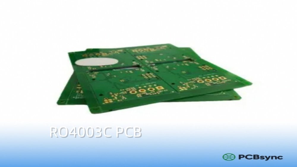
DiClad 527 vs. RO4003C
Property
DiClad 527
RO4003C
Base Material
PTFE/Woven Glass
Hydrocarbon Ceramic
Dk @ 10 GHz
2.40 – 2.65
3.38
Df @ 10 GHz
0.0022
0.0027
FR-4 Process Compatible
Limited
Yes
Relative Cost
Higher
Moderate
When to choose DiClad 527 over RO4003C: You need a lower Dk, your application is proven on PTFE materials, or you require the specific dimensional stability characteristics of woven-glass PTFE.
When to choose RO4003C instead: You want FR-4-like processing, cost is a major factor, or a Dk around 3.4 fits your design better.
DiClad 527 PCB Design Guidelines
Impedance Control Considerations
With a Dk range of 2.40–2.65, you’ll get slightly different trace widths compared to materials like RO4003C (Dk 3.38). For a 50Ω microstrip on 20-mil DiClad 527:
Trace width will be wider than on higher-Dk materials
Use your fab house’s actual Dk measurements when available
The Dk tolerance (±0.04 typical for a given Dk target) affects impedance—factor this into your tolerance analysis
Fabrication Tips for DiClad 527
Drilling: PTFE materials drill differently than FR-4. Use appropriate feed rates and spindle speeds to avoid smearing. Carbide bits work well.
Plating Adhesion: The PTFE surface can be challenging for copper adhesion. Sodium etch or plasma treatment improves bond strength. Discuss surface prep with your fab house.
Routing: Standard routing works, but take care with entry/exit points to avoid delamination.
Solder Mask: Not all solder masks adhere well to PTFE. Some designs leave the substrate unmasked (bare PTFE performs fine in many RF applications).
Stack-Up Recommendations
For multilayer designs, consider hybrid constructions pairing DiClad 527 RF layers with lower-cost materials for non-critical layers. Common bonding films include Rogers CuClad 6700 or similar PTFE-based bondplys.
How to Order DiClad 527
When specifying DiClad 527, include:
Target Dielectric Constant (within the 2.40–2.65 range)
Dielectric Thickness (0.020″, 0.030″, or 0.060″)
Copper Cladding (weight and type)
Panel Size (standard sheets: 36″×48″, 36″×72″, or 48″×54″)
Any special requirements (heavy metal backing, rolled copper, etc.)
Lead times vary—DiClad 527 isn’t as commonly stocked as RO4003C, so plan accordingly for prototypes.
Useful Resources and Downloads
Here are the official sources for DiClad 527 technical data:
Is DiClad 527 compatible with lead-free soldering?
Yes. DiClad 527 conforms to IEC 61249-2-21 and handles standard lead-free reflow profiles. The material’s thermal stability allows it to withstand the higher temperatures required for lead-free assembly without degradation.
What’s the difference between DiClad 527 and DiClad 522?
Both share the same Dk range (2.40–2.65), but DiClad 522 may have slight variations in construction. In practice, they’re often used interchangeably. Check with Rogers or your laminate supplier for current availability, as product lines evolve over time.
Can I use standard FR-4 fabrication processes with DiClad 527?
Not entirely. While some processes overlap, PTFE materials require specialized drilling parameters, surface preparation for plating adhesion, and different routing considerations. Work with a fab house experienced in PTFE materials for best results.
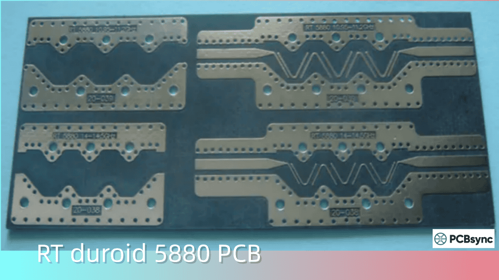
How does DiClad 527 compare to RT/duroid 5880?
RT/duroid 5880 has a lower Dk (2.20) and lower loss (Df ~0.0009), making it better for applications demanding the lowest possible insertion loss. DiClad 527 offers better mechanical properties and dimensional stability at the cost of slightly higher loss. Choose based on whether electrical performance or mechanical robustness is your priority.
What thickness should I use for my RF application?
That depends on your frequency and impedance requirements. Thinner substrates (0.020″) work well for higher frequencies and compact designs but are harder to handle. Thicker substrates (0.060″) are easier to fabricate and provide better power handling. Run your impedance calculations to determine what thickness gives you manufacturable trace widths for your target impedance.
Final Thoughts
DiClad 527 occupies a practical middle ground in the PTFE laminate world—not the absolute lowest loss, but excellent dimensional stability and mechanical properties that make fabrication more predictable. For applications like filters, couplers, and phased array elements where Dk uniformity directly affects performance, it’s a solid choice that’s proven over decades of use in demanding military and commercial RF systems.
The key is matching the material to your actual requirements. If you need rock-bottom insertion loss and can live with more challenging mechanical properties, look at DiClad 880 or RT/duroid 5880. If you want easier processing with slightly higher Dk, RO4003C might be the answer. But when you need that combination of PTFE electrical performance with the best dimensional stability the DiClad family offers, DiClad 527 delivers.
Inquire: Call 0086-755-23203480, or reach out via the form below/your sales contact to discuss our design, manufacturing, and assembly capabilities.
Quote: Email your PCB files to Sales@pcbsync.com (Preferred for large files) or submit online. We will contact you promptly. Please ensure your email is correct.
Notes: For PCB fabrication, we require PCB design file in Gerber RS-274X format (most preferred), *.PCB/DDB (Protel, inform your program version) format or *.BRD (Eagle) format. For PCB assembly, we require PCB design file in above mentioned format, drilling file and BOM. Click to download BOM template To avoid file missing, please include all files into one folder and compress it into .zip or .rar format.


