Inquire: Call 0086-755-23203480, or reach out via the form below/your sales contact to discuss our design, manufacturing, and assembly capabilities.
Quote: Email your PCB files to Sales@pcbsync.com (Preferred for large files) or submit online. We will contact you promptly. Please ensure your email is correct.
Notes: For PCB fabrication, we require PCB design file in Gerber RS-274X format (most preferred), *.PCB/DDB (Protel, inform your program version) format or *.BRD (Eagle) format. For PCB assembly, we require PCB design file in above mentioned format, drilling file and BOM. Click to download BOM template To avoid file missing, please include all files into one folder and compress it into .zip or .rar format.
Design for Testability (DFT): How to Create Easily Testable PCBs
Testing costs can consume up to 30% of your total PCB production budget. I’ve watched projects hemorrhage money because engineers treated testability as an afterthought—cramming test points into whatever space remained after routing, then discovering their boards couldn’t be tested efficiently. DFT PCB practices exist to prevent this expensive mistake by building testability into designs from the start.
After years of working with test engineers who’ve rejected designs for insufficient test access, I’ve learned that creating testable PCBs isn’t complicated—it just requires planning. This guide covers the DFT PCB principles that ensure your boards can be efficiently tested during manufacturing without requiring costly redesigns or manual workarounds.
DFT PCB—Design for Testability applied to printed circuit boards—encompasses the design practices that enable efficient verification of assembled boards. It’s the methodology ensuring every critical circuit node can be accessed, measured, and validated during manufacturing testing.
The goal is straightforward: catch defects before products ship.PCB Manufacturing introduces numerous potential failure modes—solder bridges, open connections, missing components, wrong values, reversed polarities. DFT PCB practices ensure test systems can detect these faults quickly and reliably.
The Economics of Testability
Testing economics reveal why DFT matters so much:
Test Stage
Relative Cost to Find Defect
During design review
1× (baseline)
At board assembly
10×
At system integration
100×
In the field
1,000×
Finding a $0.02 resistor with the wrong value costs almost nothing during design. Finding it after a product ships to customers costs exponentially more in returns, repairs, reputation damage, and potential liability. DFT PCB enables early detection at the assembly stage, where fixes remain affordable.
Core DFT PCB Concepts
Two fundamental principles drive all DFT decisions:
Observability: The ability to see what’s happening inside your circuit. Can you measure voltages at critical nodes? Can you verify signals are present and correct? Observability requires test points that provide electrical access to circuit nodes.
Controllability: The ability to influence circuit behavior during testing. Can you force specific inputs? Can you isolate sections for independent verification? Controllability requires design provisions like jumpers, enable pins, and partitioned power domains.
Maximizing both observability and controllability produces boards that test engineers love—and that flow through production without delays.
Types of PCB Testing Methods
Different testing methods have different DFT requirements. Understanding each method helps you design for the testing your production will actually use.
In-Circuit Testing (ICT)
In-circuit testing uses a bed-of-nails fixture with spring-loaded probes (pogo pins) that simultaneously contact test points across the entire board. The fixture clamps the PCB, establishes electrical connections, and runs comprehensive tests in seconds.
What ICT tests:
Shorts and opens between nets
Component presence and absence
Component values (resistance, capacitance)
Diode and transistor polarity
Basic IC functionality
ICT advantages:
Very fast (seconds per board)
High fault coverage (95%+ achievable)
Excellent for high-volume production
ICT limitations:
Requires custom fixture ($5,000-$50,000+)
Fixture modifications needed for design changes
Requires extensive test point access
Flying Probe Testing
Flying probe testers use movable probes (typically 4-8) that travel around the board, contacting test points sequentially. No custom fixture is required—test programs define probe movements.
Flying probe advantages:
No fixture cost
Easy program changes for design revisions
Ideal for prototypes and low-volume production
Can access tighter spaces than bed-of-nails
Flying probe limitations:
Slower than ICT (minutes per board vs. seconds)
Lower throughput for high-volume production
Still requires test point access
Boundary Scan (JTAG) Testing
Boundary scan, standardized as IEEE 1149.1 and commonly called JTAG, provides test access through dedicated pins built into compatible ICs. Test signals shift through a serial chain connecting all boundary scan devices on the board.
What boundary scan tests:
Interconnections between JTAG-compatible devices
Device presence and identity
IC pin states (stuck-at faults)
Memory and programmable device functionality
Boundary scan advantages:
No physical probe access needed for JTAG nets
Tests connections under BGAs and fine-pitch ICs
Enables in-system programming
Works throughout product lifecycle
Boundary scan limitations:
Only tests nets connected to JTAG devices
Requires JTAG-compatible components
Cannot test analog circuits directly
Functional Testing
Functional testing verifies that the assembled board performs its intended function. Test fixtures provide power, inputs, and load conditions while monitoring outputs for correct behavior.
Functional test characteristics:
Tests actual circuit operation
Validates performance specifications
Catches integration issues ICT may miss
Typically follows ICT or other structural tests
DFT PCB Test Point Design Guidelines
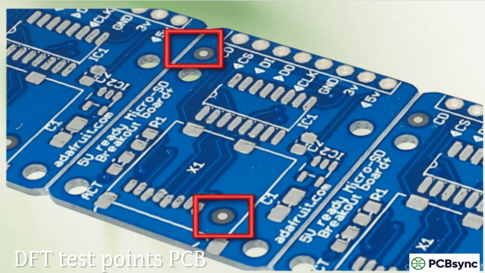
Test points are the foundation of testability. Proper test point design enables reliable probe contact and efficient testing.
Test Point Types
Type
Description
Best Use
Dedicated test pad
Round copper pad connected to net
Primary test access method
Via
Plated through-hole (untented)
Space-efficient alternative
Through-hole lead
Component pin accessible from bottom
Dual-purpose access
SMD pad extension
Extended land pattern beyond component
Fine-pitch component access
Dedicated test pads provide the most reliable contact and should be used whenever space permits. Vias work well but must remain untented (no solder mask coverage) to allow probe contact.
Test Point Size Requirements
Test Method
Minimum Pad Diameter
Recommended Diameter
Bed-of-nails ICT
0.8mm (32 mil)
1.0mm (40 mil)
Flying probe
0.5mm (20 mil)
0.75mm (30 mil)
Manual probing
1.0mm (40 mil)
1.5mm (60 mil)
Larger test points improve probe contact reliability and reduce false test failures. The 1.0mm diameter has become the de facto standard for automated testing, providing a good balance between space efficiency and contact reliability.
Test Point Spacing Requirements
Adequate spacing between test points prevents probe interference and ensures reliable contact.
Test Configuration
Minimum Center-to-Center
Recommended
Bed-of-nails (standard probes)
2.5mm (100 mil)
2.54mm (100 mil) on grid
Bed-of-nails (fine probes)
1.8mm (70 mil)
2.0mm (80 mil)
Flying probe
1.5mm (60 mil)
2.0mm (80 mil)
High-density (special probes)
1.27mm (50 mil)
1.5mm (60 mil)
Grid alignment matters: Test points aligned to a standard grid (typically 2.54mm/100 mil or 1.27mm/50 mil) simplify fixture design and reduce costs. Irregular spacing requires custom probe arrangements.
Test Point Placement Guidelines
Strategic placement ensures probe access without compromising board functionality:
Distance from components:
Minimum 2.5mm (100 mil) clearance from component edges to test point center
Minimum 5.0mm (200 mil) clearance from components taller than 6.4mm (250 mil)
Avoid placing test points under components or in shadowed areas
Distance from board edges:
Minimum 3.0mm (125 mil) from board edge to test point center
Allows vacuum seal for fixture clamping
Prevents probe access interference from fixture frame
Distribution across board:
Spread test points evenly to avoid stress concentration
Clustered test points cause board flex during fixture actuation
Keep density below 25 probes per square inch when possible
Test Point Accessibility
For most efficient testing, consolidate test access to one side of the PCB:
Single-sided probing benefits:
Simpler, less expensive fixtures
Faster fixture fabrication
More reliable probe contact
When double-sided access is necessary:
Clamshell fixtures cost significantly more
Probe alignment becomes more critical
Test time typically increases
Best practice: Place all test points on the secondary (bottom) side of the board. This keeps the primary (top) side available for component placement while providing unobstructed probe access from below.
DFT PCB Guidelines for Boundary Scan
Boundary scan testing requires specific design provisions beyond standard test points.
JTAG Chain Design
All JTAG-compatible devices connect in a daisy chain:
TDI (Test Data In) connects from first device to chain input
TDO (Test Data Out) of each device connects to TDI of the next
TCK (Test Clock) and TMS (Test Mode Select) connect in parallel to all devices
Optional TRST (Test Reset) connects in parallel if used
Chain ordering recommendations:
Group programmable devices (FPGAs, CPLDs) at one end of the chain
Provide access points between programmable and non-programmable sections
Keep similar device families together with level converters between groups
JTAG Connector Placement
Provide a dedicated JTAG connector for external test equipment access:
Pin
Signal
Notes
1
TCK
Test clock
2
GND
Ground reference
3
TDO
Data output from chain
4
VCC
Reference voltage
5
TMS
Test mode select
6
nTRST
Optional test reset
7
TDI
Data input to chain
8
GND
Ground reference
Connector placement guidelines:
Place near board edge for easy cable access
Include in schematic with clear net labeling
Document pin assignments in assembly drawings
JTAG Signal Integrity
Proper signal handling ensures reliable boundary scan operation:
Termination requirements:
Include 4.7-10kΩ pull-up on TDI (some devices lack internal pull-ups)
Include 10kΩ pull-down on TRST to keep boundary scan inactive during normal operation
Never tie TRST directly to ground—this permanently disables JTAG
Clock considerations:
Buffer TCK if driving many devices
Route TCK with controlled impedance for high-frequency operation
Beyond test points, several design practices improve overall testability.
Circuit Partitioning
Divide complex circuits into independently testable sections:
Power domain separation:
Provide separate test access for each power rail
Include current measurement points (series resistors or sense connections)
Enable individual domain power-up during testing
Functional isolation:
Use zero-ohm resistors or jumpers between major circuit sections
Allow analog and digital sections to be tested independently
Provide disable/enable controls for active circuits
Control Signal Access
Make critical control signals accessible for test manipulation:
Reset lines: Allow external reset assertion during testing
Enable pins: Provide access to chip enables for selective activation
Clock signals: Include test points on critical clocks; consider clock disable provisions
Watchdog timers: Provide disable mechanism to prevent timeouts during testing
Test Fixture Compatibility
Design for the mechanical requirements of test fixtures:
Tooling holes:
Include at least two tooling holes in opposite corners
Place asymmetrically to prevent incorrect board orientation
Use 3.0-3.2mm (125 mil) diameter for standard tooling pins
Maintain consistent locations across board revisions
Fiducials:
Include global fiducials for vision alignment
Position fiducials away from test point areas
Use same fiducial design as assembly requirements
Keep-out areas:
Reserve space for fixture push-fingers (support posts)
Distribute push-finger locations evenly across board
Maintain approximately 1.5-2.0 inch spacing between push-finger positions
Common DFT PCB Mistakes to Avoid
These frequently encountered errors cause testability problems:
Insufficient Test Coverage
Mistake: Not providing test points on all critical nets.
Consequence: Faults on untested nets escape to customers.
Prevention: Target one test point per net. Prioritize at minimum: all power rails, high-speed signals, critical control lines. Aim for 95%+ net coverage.
Test Points Under Components
Mistake: Placing test points where components block probe access.
Consequence: Probes cannot reach test points; coverage drops.
Prevention: Check component heights during layout. Maintain clearances from all components. Verify test point accessibility with 3D view before finalizing design.
Tented Vias Used as Test Points
Mistake: Specifying test point vias but allowing solder mask coverage.
Consequence: Probes contact solder mask instead of copper; tests fail or give erratic results.
Prevention: Explicitly specify “no solder mask” (untented) for all vias designated as test points. Verify in Gerber review.
Inadequate Spacing
Mistake: Placing test points too close together or too close to components.
Consequence: Probe interference, unreliable contact, or inability to build fixture.
Prevention: Follow spacing guidelines for your test method. Use design rule checks to flag violations.
Missing JTAG Access
Mistake: Using JTAG-capable devices but not implementing the chain or connector.
Consequence: Lose boundary scan coverage; cannot use JTAG for programming or debug.
Prevention: Always implement JTAG chains when devices support it. Even if not used in production test, JTAG provides valuable debug capability.
Poor Documentation
Mistake: Not documenting test point locations and net assignments.
Consequence: Test engineering wastes time extracting information; errors increase.
Prevention: Generate test point reports from CAD system. Include net names, coordinates, and test point types. Provide data in formats test fixture designers can use directly.
DFT PCB Implementation Checklist
Use this checklist during design review to verify testability:
Schematic Phase
All nets requiring test access identified
Test points added to schematic symbols
JTAG chain implemented for boundary scan devices
Control signals accessible (resets, enables, clocks)
Circuit partitioning provisions included
JTAG connector added with proper pinout
Layout Phase
Test point pads sized appropriately (1.0mm minimum)
Test point spacing meets requirements (2.5mm minimum)
Test points accessible from probe side (bottom preferred)
Component clearances maintained around test points
Tooling holes placed asymmetrically in corners
Board edge clearance maintained (3mm minimum)
Test points distributed evenly (no clusters)
Via test points not tented by solder mask
JTAG connector placed at board edge
Documentation
Test point report generated (coordinates, net names)
Test point layer clearly marked in fabrication outputs
Tooling hole locations documented
JTAG chain order documented
Special test requirements noted
Pre-Release Review
Test coverage calculated and meets target (>90%)
Design reviewed with test engineering
Fixture feasibility confirmed
High-component areas checked for probe access
Design rule check for test point violations passed
Frequently Asked Questions About DFT PCB
How many test points does my PCB need?
The goal is one test point per signal net to achieve comprehensive coverage. For most designs, this means test point quantities ranging from 100 to several hundred depending on circuit complexity. Power nets often warrant multiple test points distributed across the board for measuring voltage drops and verifying distribution. At minimum, ensure 100% coverage of power rails and 85-95% coverage of signal nets. Calculate your coverage percentage by dividing accessible nets by total nets. Work with your test engineering team to identify which nets absolutely require access versus those where test point placement isn’t practical—high-speed differential pairs, for example, may be better verified through functional testing than in-circuit probing.
What’s the difference between ICT and flying probe testing?
In-circuit testing uses a custom bed-of-nails fixture where hundreds of spring-loaded probes simultaneously contact all test points on the board, testing the entire circuit in seconds. Flying probe testing uses 4-8 movable probes that travel sequentially to test points, requiring no fixture but taking minutes per board. ICT suits high-volume production (thousands of boards) where fixture costs are amortized across many units. Flying probe suits prototypes, low-volume production, and designs with frequent revisions where fixture changes would be prohibitively expensive. Many manufacturers use both: flying probe for NPI (new product introduction) and prototypes, transitioning to ICT once designs stabilize and volumes increase. DFT requirements are similar for both, though flying probe tolerates slightly smaller test points and tighter spacing.
Should I use vias or dedicated pads as test points?
Dedicated test pads provide the most reliable probe contact and are preferred when space permits. Vias work well as a space-efficient alternative but must remain untented (no solder mask coverage) and ideally filled with solder for consistent probe contact. Through-hole component leads can serve dual purposes as test points on the solder side but become unavailable if components change to SMT. For highest reliability, use dedicated 1.0mm diameter test pads. When space constraints force via usage, specify vias as untented in your design documentation and verify this in Gerber review. Avoid using SMD component pads as test points—probing can damage solder joints, and contact reliability is poor on component leads.
Where should I place JTAG connector on my PCB?
Place the JTAG connector at a board edge where test cables can easily connect during development and production testing. Near a corner works well, keeping cables out of the way during handling. Ensure sufficient clearance around the connector for cable attachment—10mm minimum from adjacent components. Standard 2×5 or 2×10 0.1-inch headers are common; ARM’s 10-pin Cortex Debug Connector is another widely supported option. Include the connector even if production testing doesn’t require it—JTAG provides invaluable debug access during development and field troubleshooting. Document the pinout clearly in schematics and assembly drawings. For products where the connector must be removed after production, consider a pogo-pin adapter location instead of a permanent connector.
How do I calculate test coverage for my design?
Test coverage represents the percentage of potential faults your test method can detect. For in-circuit testing, calculate net coverage as: (nets with test points / total nets) × 100%. A net requires at least one test point to be testable. Generate a test point report from your CAD system showing all nets and their assigned test points; nets without assignments represent coverage gaps. For boundary scan, coverage depends on how many nets connect to JTAG-capable device pins—nets between non-JTAG devices require ICT or flying probe coverage. Industry targets typically aim for 95%+ overall coverage, with 100% coverage of power nets and critical signals. Collaborate with test engineering to identify acceptable coverage gaps; some nets may be tested functionally rather than structurally. Most CAD tools include testability analysis features that automate coverage calculations.
Useful Resources for DFT PCB Design
These resources support engineers implementing DFT practices:
Industry Standards:
IPC-9252: Guidelines and Requirements for Electrical Testing of Unpopulated Printed Boards—covers bare board testing requirements.
IEEE 1149.1: Standard Test Access Port and Boundary-Scan Architecture—the foundational JTAG specification.
IEEE 1149.6: Boundary-Scan Testing of Advanced Digital Networks—extends boundary scan for AC-coupled and differential signals.
SMTA-TP-101: Testability Guidelines—Surface Mount Technology Association guidelines for test point design.
Design Tool Resources:
Altium Designer: DFT analysis features, test point assignment, and documentation generation.
Cadence Allegro: Testability analysis, coverage reporting, and test point management.
Mentor PADS: Test preparation tools and test point optimization.
KiCad: Test point footprints and documentation export capabilities.
Test Equipment Manufacturers:
Keysight Technologies: ICT and flying probe systems with design guidelines.
Teradyne: In-circuit test platforms and DFT recommendations.
SPEA: Flying probe test systems and application notes.
Seica: Flying probe testers with design guideline documentation.
Boundary Scan Resources:
XJTAG: Comprehensive JTAG tutorials and DFT guidelines for boundary scan.
Corelis: Boundary scan education materials and design recommendations.
Asset InterTech: IEEE 1149.1 tutorial and boundary scan implementation guides.
JTAG Technologies: BSDL file resources and chain design guidance.
Online DFT Tools:
Your CM’s DFT checklist—most contract manufacturers publish specific guidelines matching their test equipment capabilities. Request these before layout begins.
BSDL file repositories—component manufacturers provide boundary scan description files required for JTAG test development. Verify availability before selecting JTAG devices.
Making DFT PCB Work in Your Design Flow
Successful DFT implementation requires early planning and cross-functional collaboration.
Start during schematic capture: Identify testability requirements before layout begins. Add test points to schematics so they appear in netlists and BOM. This ensures test access isn’t forgotten during layout optimization.
Communicate with test engineering: Your test engineers (internal or at your CM) know their equipment capabilities and constraints. Share your design early and incorporate their feedback. They can identify test access problems you might miss and suggest efficient solutions.
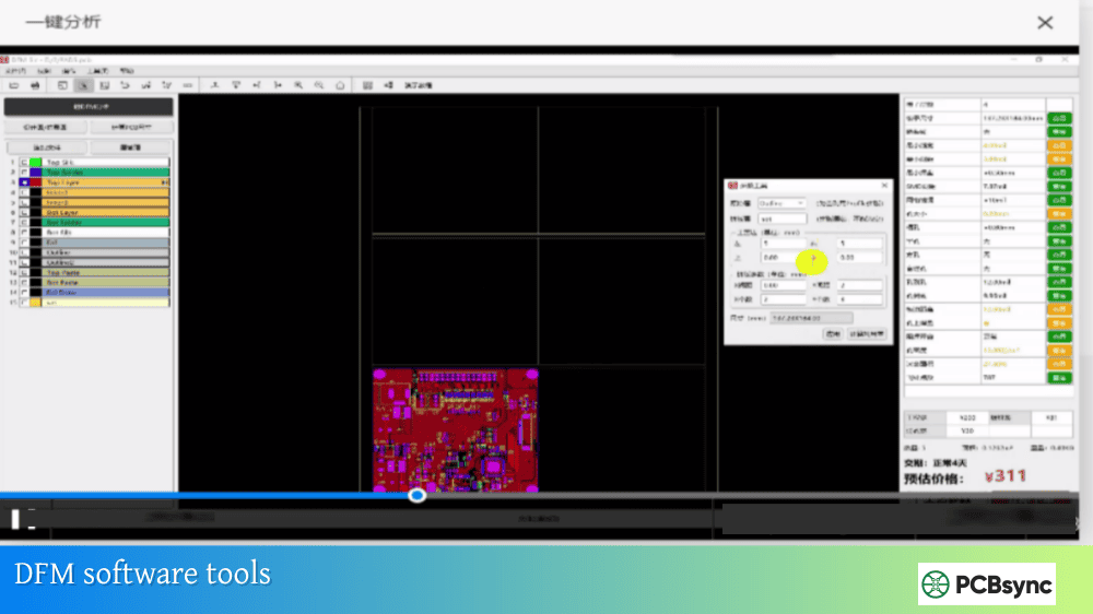
Use your CAD tools: Modern PCB design software includes testability analysis features. Enable test point DRC rules. Generate coverage reports. Use these tools to identify and fix problems before releasing designs.
Document thoroughly: Test fixture development depends on accurate, complete documentation. Generate test point files in industry-standard formats. Include net names, coordinates, pad sizes, and access side. Clear documentation accelerates fixture development and reduces errors.
Review with manufacturing: Before releasing to production, conduct a DFT review with your manufacturing partner. Confirm test point accessibility, verify fixture feasibility, and establish coverage expectations. This review catches issues when they’re still easy to fix.
DFT PCB isn’t about adding complexity—it’s about enabling efficient quality verification that protects your product and customers. The investment in testability during design pays returns throughout production: faster test cycles, higher yields, fewer escapes, and lower costs. That’s the outcome every engineer and manufacturing team wants.
Inquire: Call 0086-755-23203480, or reach out via the form below/your sales contact to discuss our design, manufacturing, and assembly capabilities.
Quote: Email your PCB files to Sales@pcbsync.com (Preferred for large files) or submit online. We will contact you promptly. Please ensure your email is correct.
Notes: For PCB fabrication, we require PCB design file in Gerber RS-274X format (most preferred), *.PCB/DDB (Protel, inform your program version) format or *.BRD (Eagle) format. For PCB assembly, we require PCB design file in above mentioned format, drilling file and BOM. Click to download BOM template To avoid file missing, please include all files into one folder and compress it into .zip or .rar format.


