Inquire: Call 0086-755-23203480, or reach out via the form below/your sales contact to discuss our design, manufacturing, and assembly capabilities.
Quote: Email your PCB files to Sales@pcbsync.com (Preferred for large files) or submit online. We will contact you promptly. Please ensure your email is correct.
Notes: For PCB fabrication, we require PCB design file in Gerber RS-274X format (most preferred), *.PCB/DDB (Protel, inform your program version) format or *.BRD (Eagle) format. For PCB assembly, we require PCB design file in above mentioned format, drilling file and BOM. Click to download BOM template To avoid file missing, please include all files into one folder and compress it into .zip or .rar format.
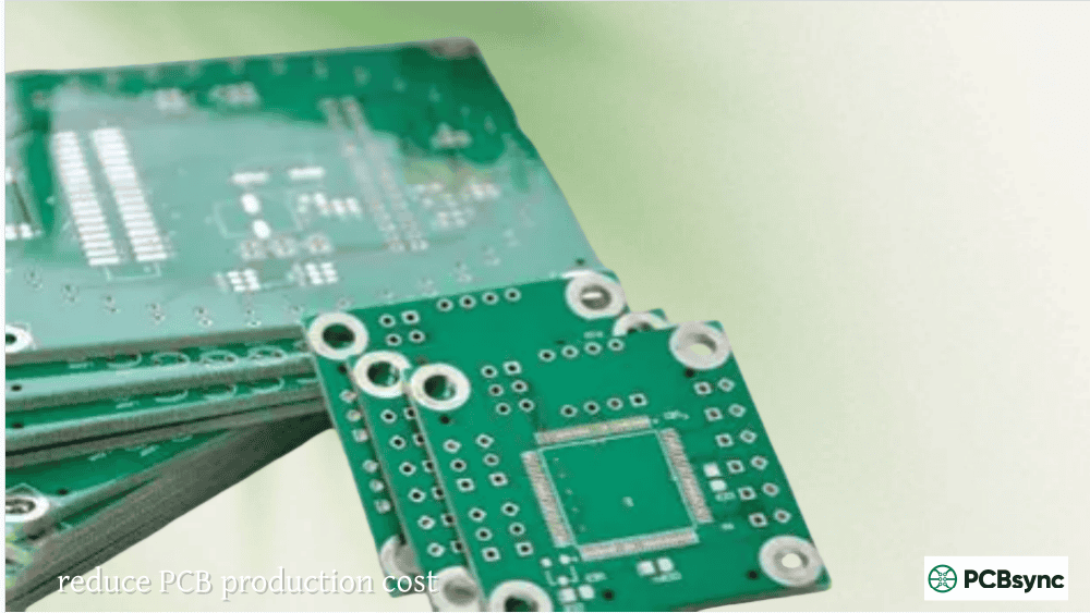
Design for Cost (DFC): How to Reduce PCB Production Expenses
Let me be honest: most PCB designers I’ve worked with over the past decade don’t think about cost until the prototype quote comes back. That’s when the panic sets in. The reality is that more than 70% of your PCB manufacturing cost gets locked in during the design phase—before you ever send files to fabrication. That’s exactly why DFC design for cost methodology has become essential to my workflow.
Design for Cost isn’t about cutting corners or sacrificing quality. It’s about making intelligent design decisions that eliminate unnecessary expenses while maintaining full functionality. When implemented properly, DFC can reduce production costs by 10-30% without changing what your board actually does.
What is Design for Cost (DFC) in PCB Manufacturing?
Design for Cost represents a systematic approach to minimizing production expenses through smart design choices made early in the development cycle. Unlike reactive cost reduction that happens after receiving a shocking quote, DFC proactively addresses cost drivers during schematic capture and PCB layout.
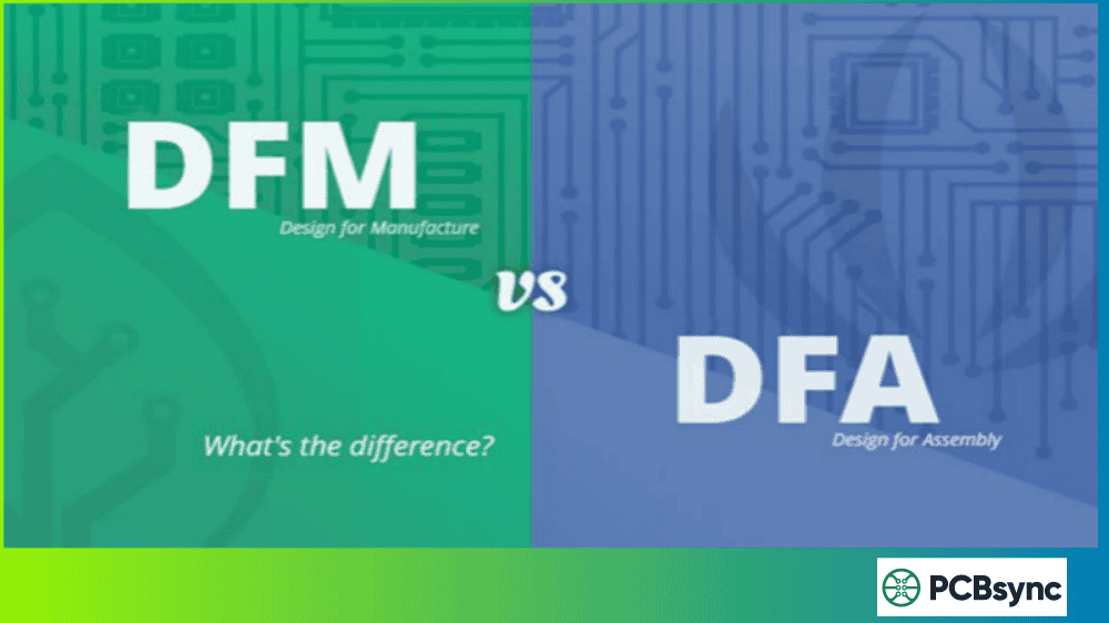
DFC design for cost is part of the broader Design for Excellence (DFX) methodology, sitting alongside Design for Manufacturing (DFM), Design for Assembly (DFA), and Design for Testability (DFT). While DFM focuses on making boards easier to produce and DFA optimizes assembly efficiency, DFC specifically targets eliminating unnecessary costs throughout the entire product lifecycle.
Why DFC Matters More Than Ever
The electronics manufacturing landscape has changed dramatically. Component shortages, supply chain volatility, and rising material costs mean that a board designed without cost awareness can quickly become unprofitable. I’ve seen projects where poor design choices added 40% to the BOM cost—expenses that were completely avoidable with proper DFC implementation.
The key insight is that cost reduction opportunities decrease dramatically as a project progresses. A design change during schematic review might cost $100. The same change after prototyping could cost $10,000. After production launch? Potentially $100,000 or more in redesign and retooling expenses.
PCB Fabrication Cost Drivers
Understanding what drives PCB fabrication cost is the foundation of effective DFC design for cost implementation. Here are the primary factors that determine what you’ll pay for bare boards:
Layer Count Optimization
Every additional layer increases fabrication cost substantially. The cost jump from 2-layer to 4-layer is significant, and costs continue climbing with each added layer pair.
Layer Count
Relative Cost
Best Application
1-layer
1.0x
Simple LED drivers, basic circuits
2-layer
1.3x
Most standard designs
4-layer
2.0-2.5x
Mixed-signal, moderate complexity
6-layer
3.0-3.5x
High-speed digital, dense routing
8+ layers
4.0x+
Complex HDI, high-frequency RF
Before automatically reaching for more layers, ask yourself: can I achieve proper routing with better component placement? I’ve redesigned 6-layer boards down to 4 layers simply by optimizing component locations—saving 30% on fabrication cost.
Board Size and Panelization
PCB cost scales with area, but the relationship isn’t always linear. Manufacturers work with standard panel sizes, and your board placement on those panels determines material utilization. A board that’s 101mm x 101mm might cost significantly more than one at 99mm x 99mm simply because of panel utilization efficiency.
Work with your manufacturer to optimize board dimensions for their standard panel sizes. Sometimes reducing board area by 5% can cut fabrication cost by 15% or more through improved panel utilization.
Via Technologies
Via selection dramatically impacts fabrication cost and should be a primary consideration in your DFC design for cost strategy:
Via Type
Cost Impact
When to Use
Through-hole vias
Baseline
Default choice for most designs
Buried vias
2-3x increase
Only when routing density absolutely requires
Blind vias
2-3x increase
High-density interconnect applications
Microvias (laser drilled)
3-4x increase
HDI designs with BGAs
Via-in-pad (filled/capped)
1.5-2x increase
Fine-pitch BGA escape routing
The rule here is simple: use through-hole vias unless your design absolutely cannot route without advanced via technologies. Many designers default to via-in-pad for BGA escape routing when standard dogbone patterns would work perfectly well.
Standard vs. Custom Specifications
Manufacturers optimize their processes for standard specifications. Any deviation triggers additional cost:
Specification
Standard (Low Cost)
Custom (Higher Cost)
Board thickness
1.6mm
<1.2mm or >2.0mm
Copper weight
1oz (35μm)
2oz+ or <0.5oz
Solder mask color
Green
Black, red, blue, white
Surface finish
HASL
ENIG, OSP, immersion silver
Minimum trace/space
6/6 mil (0.15mm)
<5/5 mil
Minimum hole size
0.3mm
<0.25mm
Board shape
Rectangle
Irregular, internal cutouts
Stick with standard specifications whenever possible. That fancy matte black solder mask might look great, but it adds 10-20% to your fabrication cost with zero functional benefit.
BOM Optimization Strategies for DFC
Component costs typically represent 50-70% of total PCBA cost, making BOM optimization the highest-impact area for DFC design for cost implementation.
Component Standardization
One of the most effective cost reduction strategies is standardizing components across your product line. Using the same 10kΩ resistor across five different products instead of five different part numbers consolidates purchasing volume and simplifies inventory management.
Create an approved parts list with preferred components in each category. When designers need a 100nF capacitor, they should reach for the standard part number rather than selecting whatever appears first in the component library.
Package Size Selection
Component package size affects both BOM cost and assembly cost:
Passive Package
BOM Cost
Assembly Cost
Recommendation
0201
Higher
Higher (precision placement)
Avoid unless space-critical
0402
Moderate
Moderate
Good balance for dense boards
0603
Lower
Lower
Default choice for most designs
0805
Lowest
Lowest
Best for hand assembly, prototypes
The sweet spot for most production designs is 0603 for passives. Going smaller than 0402 typically increases both component and assembly costs due to precision handling requirements.
Lifecycle Awareness
Component obsolescence can devastate your DFC efforts. Designing with end-of-life (EOL) components means forced redesigns, premium pricing for last-time buys, and potential production delays.
Check component lifecycle status during design:
Active: Preferred choice for new designs
NRND (Not Recommended for New Designs): Avoid—likely approaching EOL
EOL: Never use in new designs
Obsolete: Requires immediate alternate sourcing
Modern BOM management tools like Altium’s ActiveBOM or Octopart’s API integration flag lifecycle risks automatically. Use them.
Second Source Strategy
Single-source components create supply chain risk and eliminate pricing leverage. For every critical component, identify at least one alternate source with equivalent specifications.
This doesn’t mean designing for two different part numbers—it means confirming that pin-compatible, specification-equivalent alternatives exist from different manufacturers before committing to a design.
Assembly costs depend heavily on design decisions made during PCB layout. Here’s how to minimize them:
Single-Sided vs. Double-Sided Assembly
Double-sided assembly requires the board to pass through the reflow oven twice, doubling thermal stress and processing time. If your design can fit on one side, the assembly cost reduction can be substantial—often 20-30%.
When double-sided placement is unavoidable, minimize bottom-side components and group them strategically to optimize the assembly process.
Component Orientation Standardization
Automated pick-and-place machines work most efficiently when similar components share the same orientation. Rotating components arbitrarily during layout creates unnecessary machine movements and increases assembly time.
Establish orientation standards:
Polarized components (tantalum capacitors, diodes): cathode facing one direction
ICs: pin 1 toward top or left edge consistently
Passives: aligned horizontally or vertically, not mixed
Reducing Component Variety
Every unique part number in your BOM adds setup time, feeder allocation, and inventory complexity. A board with 50 unique part numbers costs more to assemble than one with 30 unique parts, even if the total component count is identical.
Consolidate where possible:
Use one resistor value for multiple non-critical pull-ups/pull-downs
Standardize on common capacitor values (100nF, 10μF) rather than calculated ideal values
Select IC packages that accommodate multiple functions
DFC Design for Cost Checklist
Use this checklist during design reviews to ensure cost optimization:
Fabrication Optimization
Minimum layer count for required routing
Board dimensions optimized for panel utilization
Through-hole vias used unless HDI required
Standard board thickness (1.6mm)
Standard copper weight (1oz)
Green solder mask selected
6/6 mil minimum trace/space or greater
No unnecessary internal cutouts
BOM Optimization
Component lifecycle status verified (no NRND/EOL parts)
PCBWay Instant Quote: Real-time pricing for fabrication options
JLCPCB Calculator: Quick cost estimates with specification options
Sierra Circuits Quote Tool: Detailed breakdown of cost drivers
BOM Management Software
Altium ActiveBOM: Integrated lifecycle and pricing data
Octopart: Cross-distributor pricing comparison
Digi-Key BOM Manager: Availability and pricing aggregation
FindChips: Component search across distributors
Industry Standards References
IPC-2221: Generic Standard on Printed Board Design
IPC-2222: Sectional Design Standard for Rigid Organic Printed Boards
IPC-7351: Generic Requirements for Surface Mount Design and Land Pattern Standard
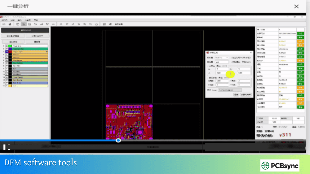
DFM/DFA Analysis Tools
Valor NPI (Siemens): Comprehensive DFM analysis
CAM350 (DownStream): Gerber analysis and optimization
FreeDFM (Advanced Circuits): Online DFM check service
Frequently Asked Questions About DFC Design for Cost
What is the difference between DFC and DFM?
Design for Cost (DFC) specifically focuses on minimizing production expenses through component selection, specification optimization, and lifecycle management. Design for Manufacturing (DFM) ensures designs can be produced efficiently with high yield. While related, DFC addresses “how much will this cost?” while DFM addresses “can this be built reliably?” Both are essential components of the broader Design for Excellence (DFX) methodology.
When should DFC be implemented in the design process?
DFC should begin during concept and schematic phases—the earlier, the better. By the time layout is complete, approximately 70% of manufacturing cost is already locked in. Waiting until prototype quotes arrive to consider cost means missing the majority of optimization opportunities. Review component selections for cost impact before schematic completion, and verify fabrication specifications during early layout stages.
How much can DFC actually save on PCB production?
Results vary by design complexity and starting point, but well-implemented DFC typically reduces total PCBA cost by 10-30%. I’ve seen individual design changes save 40% or more—switching from a 6-layer board to 4-layer, eliminating via-in-pad requirements, or consolidating component values. The key is that small savings across many design decisions accumulate into significant total cost reduction.
Does DFC compromise product quality or reliability?
Properly implemented DFC should never compromise quality. The goal is eliminating unnecessary costs, not cutting corners on functional requirements. Using green solder mask instead of black doesn’t affect reliability. Selecting components with active lifecycle status rather than EOL parts actually improves long-term reliability. However, attempting to reduce costs by violating design rules, using substandard components, or eliminating necessary testing will inevitably create quality problems.
How do I balance DFC with aggressive project schedules?
DFC doesn’t require significant additional time when integrated into standard design workflows. The key is having component databases with pricing and lifecycle data readily available, maintaining approved parts lists, and running DFM checks as part of the normal design review process. Most DFC decisions take seconds when the right information is at hand. The alternative—redesigning a board after receiving an unexpectedly high production quote—takes far more time than proactive cost optimization.
Building Cost Awareness Into Your Design Culture
The most successful DFC implementations happen when cost awareness becomes part of the design culture, not a separate review step. When every engineer understands that component choices, via types, and layer count decisions have direct cost implications, optimization happens naturally throughout the design process.
Start by making cost data visible during design. Display component pricing in schematic tools. Run fabrication cost estimates during layout, not after completion. Celebrate designs that achieve functionality at lower cost, not just those that work.
DFC design for cost isn’t about being cheap—it’s about being smart. Every dollar saved on unnecessary specifications or overdesigned features is a dollar available for features that actually matter to your customers. In today’s competitive market, that efficiency isn’t optional; it’s essential for survival.
The boards that win in the marketplace aren’t necessarily the most sophisticated designs. They’re the ones that deliver required functionality at sustainable cost points. Master DFC, and you’ll build products that succeed not just technically, but commercially.
Inquire: Call 0086-755-23203480, or reach out via the form below/your sales contact to discuss our design, manufacturing, and assembly capabilities.
Quote: Email your PCB files to Sales@pcbsync.com (Preferred for large files) or submit online. We will contact you promptly. Please ensure your email is correct.
Notes: For PCB fabrication, we require PCB design file in Gerber RS-274X format (most preferred), *.PCB/DDB (Protel, inform your program version) format or *.BRD (Eagle) format. For PCB assembly, we require PCB design file in above mentioned format, drilling file and BOM. Click to download BOM template To avoid file missing, please include all files into one folder and compress it into .zip or .rar format.


