Inquire: Call 0086-755-23203480, or reach out via the form below/your sales contact to discuss our design, manufacturing, and assembly capabilities.
Quote: Email your PCB files to Sales@pcbsync.com (Preferred for large files) or submit online. We will contact you promptly. Please ensure your email is correct.
Notes: For PCB fabrication, we require PCB design file in Gerber RS-274X format (most preferred), *.PCB/DDB (Protel, inform your program version) format or *.BRD (Eagle) format. For PCB assembly, we require PCB design file in above mentioned format, drilling file and BOM. Click to download BOM template To avoid file missing, please include all files into one folder and compress it into .zip or .rar format.
Design Raspberry Pi HATs & Pico Add-ons in EasyEDA: Complete Tutorial
There’s something incredibly satisfying about designing a custom add-on board for your Raspberry Pi and seeing it arrive as a professionally manufactured PCB. I’ve been through this process dozens of times, and I can tell you that EasyEDA Raspberry Pi projects are among the most rewarding designs you can tackle as a PCB engineer or hobbyist.
Whether you’re creating an EasyEDA Raspberry Pi HAT for a sensor array, motor controller, or audio interface—or designing a compact expansion board for the EasyEDA Raspberry Pi Pico—this guide covers everything you need to know. We’ll walk through the entire workflow from understanding specifications to getting your boards manufactured and assembled.
Before diving into the technical details, let’s talk about why EasyEDA makes such a good choice for Raspberry Pi add-on board design.
EasyEDA is a free, cloud-based PCB design tool that integrates directly with JLCPCB for manufacturing and LCSC for components. This tight integration means you can go from idea to professionally manufactured boards in a matter of days, often for just a few dollars. The platform includes over 700,000 components in its library, many with verified footprints specifically tested with JLCPCB’s assembly service.
For Raspberry Pi projects specifically, EasyEDA offers several advantages:
Pre-made templates and footprints for Pi HATs and Pico modules
Community-contributed libraries with hundreds of Pi-related components
Direct access to JLCPCB assembly parts (important when you want your HAT manufactured and assembled)
Free 3D preview to verify your board fits correctly on the Pi
Seamless Gerber export optimized for JLCPCB production
The learning curve is gentle enough for beginners while offering sufficient depth for complex multi-layer designs.
Understanding Raspberry Pi HAT Specifications
If you want your board to officially qualify as a HAT (Hardware Attached on Top), there are specific requirements you must follow. The Raspberry Pi Foundation maintains these specifications to ensure compatibility and a consistent user experience.
Official HAT Mechanical Requirements
Specification
Requirement
Board Dimensions
65mm × 56mm
Mounting Holes
4 holes, 2.75mm diameter, aligning with Pi mounting holes
Corner Radius
Rounded corners (3mm radius recommended)
GPIO Connector
Full 40-pin header
Minimum Spacing
At least 8mm from Pi (10-12mm recommended)
PoE Header Clearance
Must not foul Pi 3B+/4B/5 PoE header
HAT Electrical Requirements
Beyond mechanical specs, there are important electrical considerations:
ID EEPROM: A true HAT must include an ID EEPROM connected to GPIO0 (ID_SD) and GPIO1 (ID_SC). This EEPROM stores vendor information, GPIO configuration, and device tree data that allows the Pi to automatically configure itself at boot.
EEPROM Pull-ups: GPIO0 and GPIO1 require 3.9KΩ pull-up resistors to 3.3V. These are the only permitted connections to these pins besides the EEPROM itself.
Back-powering Safety: If your HAT supplies power to the Pi through the GPIO header, you must include a reverse current protection diode and be able to supply at least 1.3A (2A recommended) continuously.
GPIO Boot State Protection: During boot, GPIO6, GPIO14, and GPIO16 may briefly become outputs on older firmware. Your circuit should tolerate or protect against this.
pHAT and uHAT Form Factors
Not every project needs the full HAT size. Smaller form factors are available:
Form Factor
Dimensions
Notes
HAT
65mm × 56mm
Full size, requires 4 mounting holes
pHAT
65mm × 30mm
Pi Zero compatible, narrower
uHAT (Micro HAT)
40mm × 30mm
Minimal footprint
For pHATs and uHATs, you still follow the same electrical specifications—the only difference is the board size and number of mounting holes.
Setting Up Your EasyEDA Raspberry Pi HAT Project
Let’s walk through creating a HAT design from scratch in EasyEDA.
Step 1: Create a New Project
Log into EasyEDA (either the web version or desktop client) and create a new project. I recommend naming it descriptively—something like “SensorHAT_v1” rather than just “HAT.”
Go to File → New → Project and give it a name. Then create a new schematic within that project (File → New → Schematic).
Step 2: Find the 40-Pin Header Component
The heart of any HAT design is the 40-pin GPIO header. In EasyEDA:
Open the Libraries panel (press L or click the library icon)
Search for “Raspberry Pi 40 pin header” or “2×20 pin header”
Look for components with the JLCPCB Assembly icon if you want your boards assembled
Place the header on your schematic
Several community-contributed templates exist specifically for HAT designs. Search for “Raspberry Pi HAT template” in the EasyEDA library or OSHWLab to find starting points that include the correct board outline, mounting holes, and GPIO header already positioned.
Step 3: Add the ID EEPROM Circuit (Optional but Recommended)
For a proper HAT, add the ID EEPROM circuit:
EEPROM: CAT24C32 or similar I2C EEPROM (24C32/24C64 are common choices)
Pull-up resistors: 2× 3.9KΩ to 3.3V on ID_SD and ID_SC
Decoupling capacitor: 100nF on EEPROM VCC
Connect the EEPROM’s SDA to GPIO0 (Pin 27) and SCL to GPIO1 (Pin 28). These pins are dedicated to HAT identification and should not be used for other purposes.
Step 4: Design Your Circuit
Now add your application-specific circuitry. A few tips for HAT designs:
Power considerations: If your circuit needs 5V, tap it from GPIO pins 2 and 4. For 3.3V, use pins 1 and 17. Always ensure your power draw is within the Pi’s supply capability.
I2C devices: Use GPIO2 (SDA1) and GPIO3 (SCL1) for I2C peripherals. These have on-board 1.8KΩ pull-ups to 3.3V already.
SPI devices: SPI0 uses GPIO10 (MOSI), GPIO9 (MISO), GPIO11 (SCLK), and GPIO8/7 for CE0/CE1.
UART: GPIO14 (TXD) and GPIO15 (RXD) provide serial communication. Note that GPIO14 is one of the pins that may briefly go high during boot.
Step 5: Convert to PCB and Set Board Outline
Once your schematic is complete:
Click Design → Convert to PCB
In the PCB editor, draw the board outline on the Board Outline layer
For a full HAT: create a 65mm × 56mm rectangle with 3mm corner radius
Add four 2.75mm mounting holes at the standard positions
The mounting hole positions (measured from the bottom-left corner) are:
Hole
X Position
Y Position
1
3.5mm
3.5mm
2
61.5mm
3.5mm
3
3.5mm
52.5mm
4
61.5mm
52.5mm
Step 6: Place and Route Components
Position your components logically:
Place the 40-pin header in its standard position (aligning with the GPIO header location)
Keep high-frequency components close to the header
Route power traces wider than signal traces (0.4mm minimum for power, 0.254mm for signals is typical)
Use a ground plane on at least one layer for better EMI performance
Use EasyEDA’s Design Rule Check (DRC) to verify your layout meets manufacturing constraints. For JLCPCB, the standard minimums are 0.127mm trace width and 0.127mm spacing.
Designing Raspberry Pi Pico Add-on Boards in EasyEDA
The EasyEDA Raspberry Pi Pico workflow differs from HAT design since the Pico is a microcontroller board rather than a single-board computer. You have two main options: design a carrier board for the Pico module, or design around the RP2040 chip directly.
Understanding Pico Module Dimensions
The Raspberry Pi Pico (and Pico 2) has a unique form factor that supports multiple mounting methods:
Specification
Value
Board Size
51mm × 21mm × 1mm
Pin Pitch
2.54mm (0.1″) standard
Total Pins
40 (20 per side)
Mounting Holes
4× 2.1mm diameter
Edge Type
Castellated + through-hole
The castellated edges are what make the Pico special—you can either solder it directly to a carrier board (SMD style) or use pin headers for removable mounting.
EasyEDA’s library includes several Raspberry Pi Pico components:
Search “Raspberry Pi Pico” in the Libraries panel
You’ll find options for:
Through-hole mounting (using pin headers)
SMD/castellated mounting (soldering directly to carrier)
Pico W variants (with WiFi)
Pico 2 variants (RP2350-based)
Choose the footprint that matches your intended mounting method. For prototyping, through-hole is easier. For production, SMD mounting creates a more compact and robust assembly.
Pico Carrier Board Design Tips
When designing a carrier board for the Pico:
Power supply considerations: The Pico has an onboard buck-boost regulator that accepts 1.8V to 5.5V input on VSYS. Don’t apply power to both USB and VSYS simultaneously unless you add proper protection.
GPIO voltage: All Pico GPIOs are 3.3V only. Do not connect 5V signals directly—use level shifters if needed.
ADC inputs: The Pico has 4 ADC channels (GPIO26-29) with 12-bit resolution. Keep analog traces short and away from digital signals.
USB breakout: If your carrier needs USB, you can either use the Pico’s micro-USB connector or break out the USB signals (GPIO TP2 and TP3) to your own connector.
Debug access: Consider breaking out the SWD pins (SWDIO, SWCLK, GND) to a header for programming and debugging.
Creating a Pico Expansion Board: Practical Example
Let’s design a simple sensor expansion board for the Pico:
Step 1: Create a new EasyEDA project and schematic.
Step 2: Place the Pico module component. Search for “Raspberry Pi Pico TH/SMD” for a versatile footprint.
Step 3: Add your peripheral circuits. For this example:
BME280 environmental sensor (I2C on GPIO4/5)
WS2812B addressable LED (data on GPIO16)
Two tactile buttons (GPIO14 and GPIO15)
Power LED on 3.3V
Step 4: Wire everything using EasyEDA’s wire tool. Add net labels for clarity.
Step 5: Convert to PCB and create a board outline. A 60mm × 40mm board gives plenty of room.
Step 6: Position the Pico footprint centrally, with the USB connector facing the edge.
Step 7: Route traces. Use 0.3mm traces for signals and 0.5mm for power.
Step 8: Add silkscreen labels for GPIO numbers and component positions.
Working with EasyEDA’s Component Library for Pi Projects
One of EasyEDA’s strengths is its extensive component library. Here’s how to effectively use it for Raspberry Pi projects.
Finding JLCPCB Assembly-Compatible Parts
If you want your boards assembled by JLCPCB:
In the Library panel, filter by “LCSC Assembled”
Look for the SMT icon indicating assembly availability
Check whether the part is “Basic” (no setup fee) or “Extended” ($3 setup fee per unique part)
For cost-effective designs, try to use Basic parts for common components like resistors, capacitors, and common ICs.
Community Templates for Raspberry Pi
EasyEDA’s community has contributed numerous Raspberry Pi templates:
HAT Templates: Pre-made board outlines with mounting holes and GPIO header
Pico Modules: Various footprint options for different mounting styles
Pi Zero Templates: Smaller form factor for Zero/Zero W projects
Search OSHWLab (oshwlab.com) for “Raspberry Pi” to find complete open-source projects you can clone and modify.
Creating Custom Components
Sometimes you’ll need components not in the library. To create a custom symbol and footprint:
File → New → Symbol (for schematic symbol)
File → New → Footprint (for PCB footprint)
Use the Footprint Manager to link them together
Save to your personal library
For Raspberry Pi projects, you might need custom footprints for:
Specific connector types
Custom sensor modules
Specialized display connectors
Manufacturing Your Raspberry Pi Add-on Board
Once your design is complete, it’s time to manufacture.
Exporting Gerber Files
EasyEDA makes Gerber export straightforward:
In the PCB editor, go to Fabrication → PCB Fabrication File (Gerber)
Review the preview to ensure all layers look correct
Download the Gerber ZIP file
Ordering from JLCPCB
The direct integration with JLCPCB streamlines ordering:
Click “Order at JLCPCB” in EasyEDA
Your Gerber files upload automatically
Choose PCB specifications:
Layers: 2 (sufficient for most HATs)
Thickness: 1.6mm (standard)
Color: Green is cheapest, other colors add small cost
Surface Finish: HASL (lead-free recommended)
For HATs specifically, 1.6mm thickness is standard and ensures proper alignment with the Pi’s mounting holes.
Using JLCPCB Assembly Service
For assembled boards:
Enable “SMT Assembly” in the order form
Upload your BOM (Bill of Materials) file
Upload your CPL (Component Placement List) file
Select which parts to assemble
EasyEDA generates JLCPCB-compatible BOM and CPL files directly:
Fabrication → BOM
Fabrication → Pick and Place File
Review the part matching carefully. JLCPCB’s system will show you any parts that don’t have exact matches, and you can substitute equivalents.
Useful Resources for EasyEDA Raspberry Pi Development
Here are the essential resources for your projects:
Official Documentation
Resource
URL
Description
HAT+ Specification
datasheets.raspberrypi.com
Official HAT design requirements
Pico Datasheet
datasheets.raspberrypi.com
Pico dimensions and pinout
EasyEDA Tutorials
docs.easyeda.com
Complete EasyEDA documentation
JLCPCB Capabilities
jlcpcb.com
Manufacturing specifications
Footprint and Template Libraries
Source
URL
Content
EasyEDA Library
easyeda.com/components
Official component library
OSHWLab
oshwlab.com
Community open-source projects
Raspberry Pi GPIO Pinout
pinout.xyz
Interactive GPIO reference
LCSC Components
lcsc.com
Parts database with datasheets
Design Files and Templates
Resource
Description
Raspberry Pi HAT Templates
Search “HAT template” in EasyEDA
Pico Footprints
Search “Raspberry Pi Pico” in library
KiCad Pi Libraries
Available on GitHub (can convert to EasyEDA)
SnapEDA
snapeda.com – verified footprints
Community Resources
Raspberry Pi Forums (forums.raspberrypi.com) – Active community for hardware questions
EasyEDA Forum (easyeda.com/forum) – EasyEDA-specific help
r/raspberry_pi on Reddit – Community projects and advice
GitHub – Search for “raspberry pi hat easyeda” for open-source projects
Common Design Mistakes to Avoid
After designing numerous Pi add-on boards, here are the pitfalls I see most often:
Wrong header orientation: Double-check that pin 1 of your GPIO header matches pin 1 on the Pi. Getting this wrong means a completely non-functional (or damaged) board.
Insufficient clearance for USB/Ethernet: On full-size Pi models, ensure your HAT doesn’t block the USB and Ethernet ports on the opposite side.
Forgetting PoE header clearance: Pi 3B+, 4B, and 5 have a 4-pin PoE header that your HAT must not obstruct.
Wrong mounting hole sizes: Use 2.75mm holes, not 3mm. The extra tolerance matters for proper alignment.
ID_SD/ID_SC conflicts: If you’re using I2C devices, don’t connect them to GPIO0/1—those are reserved for the ID EEPROM.
Power draw exceeding limits: The 3.3V rail from the Pi can supply limited current. For high-power projects, add your own regulation.
Frequently Asked Questions
Can I design a Raspberry Pi HAT in EasyEDA without following the official specification?
Yes, you can design any add-on board for the Pi using EasyEDA. However, you can only call it a “HAT” if it meets all official requirements including the ID EEPROM, specific dimensions, and mounting holes. Non-compliant boards are simply called “add-on boards” or “shields.”
Does EasyEDA have official Raspberry Pi Pico footprints?
EasyEDA’s library includes multiple community-contributed Pico footprints for both through-hole and SMD mounting. Search for “Raspberry Pi Pico” in the library. While not officially from Raspberry Pi, these footprints are based on the official datasheet dimensions and are verified by the community.
How do I ensure my HAT components are available for JLCPCB assembly?
When selecting components, filter the EasyEDA library by “LCSC Assembled” to show only parts that JLCPCB can assemble. Check each component’s availability and whether it’s a Basic or Extended part. Basic parts have no setup fee; Extended parts add $3 per unique component type.
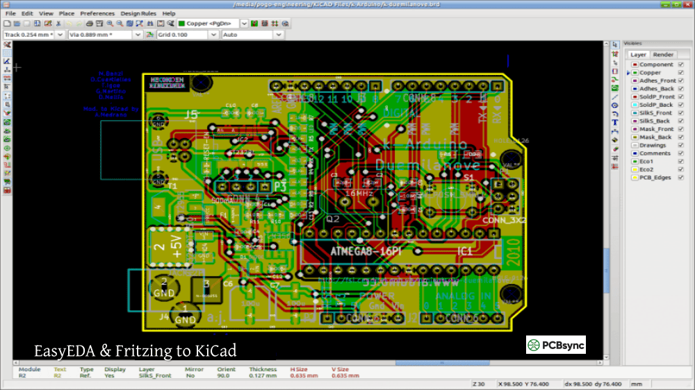
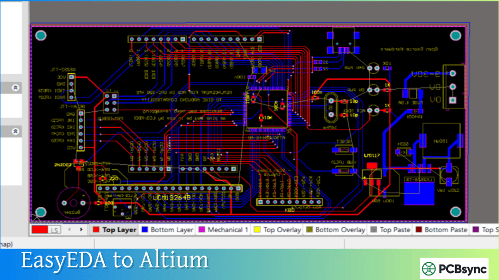
Can I use KiCad Raspberry Pi libraries in EasyEDA?
EasyEDA can import Eagle format libraries (.lbr). While it doesn’t directly import KiCad libraries, many KiCad libraries have been converted and uploaded to EasyEDA’s community library. You can also convert KiCad libraries to Eagle format first, then import into EasyEDA.
What’s the minimum order quantity for Raspberry Pi HAT PCBs from JLCPCB?
JLCPCB’s minimum order is 5 PCBs. For boards up to 100mm × 100mm (which includes standard HAT dimensions), the cost is typically around $2-5 for 5 boards plus shipping. Assembly minimum is also 5 boards.
Conclusion
Designing EasyEDA Raspberry Pi add-on boards—whether full HATs, pHATs, or Pico expansion boards—is remarkably accessible with modern tools. EasyEDA’s free platform, combined with JLCPCB’s affordable manufacturing, makes it possible for anyone to create professional-quality custom hardware.
The key is understanding the specifications before you start. For HATs, that means the precise mechanical dimensions, mounting hole positions, and ID EEPROM requirements. For Pico add-ons, it’s about choosing the right mounting method and respecting the module’s power and voltage requirements.
Start with a simple project—perhaps an LED indicator HAT or a button expansion for the Pico. Once you’ve been through the complete cycle from schematic to manufactured board, you’ll have the confidence to tackle more complex designs. The Raspberry Pi community is incredibly supportive, and there are countless open-source projects on OSHWLab and GitHub that you can learn from or build upon.
Your first EasyEDA Raspberry Pi HAT or EasyEDA Raspberry Pi Pico expansion might take a weekend to design. But once you hold that professionally manufactured board in your hands and plug it into your Pi, you’ll understand why so many engineers and hobbyists find this process addictive.
Inquire: Call 0086-755-23203480, or reach out via the form below/your sales contact to discuss our design, manufacturing, and assembly capabilities.
Quote: Email your PCB files to Sales@pcbsync.com (Preferred for large files) or submit online. We will contact you promptly. Please ensure your email is correct.
Notes: For PCB fabrication, we require PCB design file in Gerber RS-274X format (most preferred), *.PCB/DDB (Protel, inform your program version) format or *.BRD (Eagle) format. For PCB assembly, we require PCB design file in above mentioned format, drilling file and BOM. Click to download BOM template To avoid file missing, please include all files into one folder and compress it into .zip or .rar format.


