Inquire: Call 0086-755-23203480, or reach out via the form below/your sales contact to discuss our design, manufacturing, and assembly capabilities.
Quote: Email your PCB files to Sales@pcbsync.com (Preferred for large files) or submit online. We will contact you promptly. Please ensure your email is correct.
Notes: For PCB fabrication, we require PCB design file in Gerber RS-274X format (most preferred), *.PCB/DDB (Protel, inform your program version) format or *.BRD (Eagle) format. For PCB assembly, we require PCB design file in above mentioned format, drilling file and BOM. Click to download BOM template To avoid file missing, please include all files into one folder and compress it into .zip or .rar format.
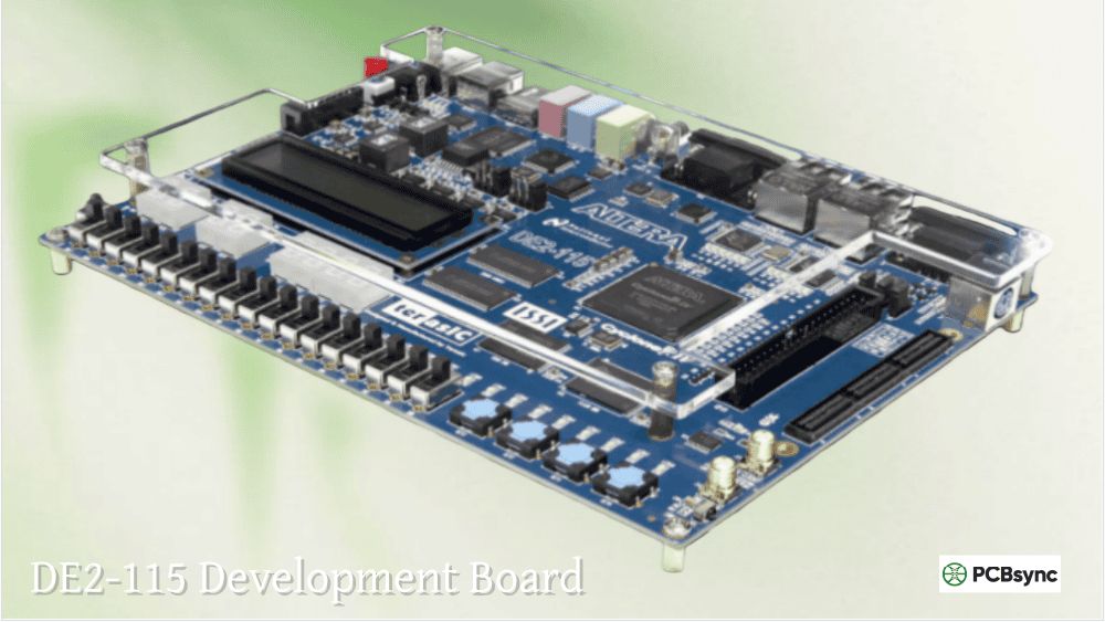
Altera DE2-115 FPGA Board: Features, Price, Projects & Getting Started
If you’ve been looking for a feature-rich FPGA development board for education or prototyping, chances are the DE2-115 has come up in your research. I’ve worked with this board extensively over the years, and it remains one of the most capable educational platforms despite being based on the older Cyclone IV architecture. The sheer number of onboard peripherals makes the Altera DE2-115 a versatile workhorse for everything from digital logic courses to advanced embedded system prototyping.
This comprehensive guide covers everything you need to know about the Terasic DE2-115 board—from detailed specifications and pricing to practical project ideas and step-by-step setup instructions. Whether you’re a student purchasing your first FPGA board or an engineer evaluating platforms for a university lab, you’ll find the information you need here.
The DE2-115 FPGA development board is manufactured by Terasic and designed specifically for educational institutions and development purposes. It features the Altera (now Intel) Cyclone IV EP4CE115 FPGA—the largest device in the Cyclone IV E series with 114,480 logic elements.
The board evolved from Terasic’s earlier DE2 series, building on the success of the DE2-70 while adding modern interfaces like Gigabit Ethernet. The naming convention “115” refers to the approximate logic element count (114,480 LEs), helping distinguish it from smaller variants.
What makes the Altera DE2-115 FPGA particularly attractive for education is its “kitchen sink” approach to peripherals. Rather than providing a minimal FPGA with expansion headers, Terasic packed the board with practically every interface you might need for coursework—from simple LEDs and switches to VGA output, audio codecs, and dual Gigabit Ethernet ports.
Key Advantages of the DE2-115 Platform
From my experience using this board in both teaching and prototyping environments, several characteristics stand out:
The FPGA Altera DE2-115 provides enough logic resources for substantial designs. With 114,480 LEs and 3.9 Mbits of embedded RAM, you can implement complete soft-core processor systems with room to spare for custom peripherals.
The diversity of onboard I/O eliminates the need for purchasing separate daughter cards for most educational projects. Students can work with VGA graphics, audio processing, Ethernet communication, and SD card storage without any additional hardware investment.
Extensive documentation and example designs from both Terasic and Intel’s University Program significantly reduce the learning curve. The board has been used in universities worldwide for over a decade, creating a substantial community knowledge base.
DE2-115 FPGA Technical Specifications
Understanding the full capabilities of the DE2-115 Terasic board requires examining its specifications in detail. The following tables break down the major subsystems.
FPGA Device Specifications
Specification
Value
FPGA Device
Cyclone IV EP4CE115F29C7
Logic Elements (LEs)
114,480
Embedded Memory
3,888 Kbits
Embedded Multipliers
266 (18×18)
PLLs
4 General-purpose
User I/O Pins
528
Configuration Device
EPCS64 (64Mbit serial)
Memory Subsystem
The DE2-115 provides a generous complement of memory options for various application requirements:
Memory Type
Capacity
Organization
Interface
SDRAM
128 MB
32M × 32-bit
32-bit bus
SRAM
2 MB
1M × 16-bit
16-bit bus
Flash
8 MB
4M × 16-bit
8-bit mode
EEPROM
32 Kbit
I2C
Serial
The 128MB SDRAM is particularly valuable for Nios II soft-core processor designs where you need substantial program and data storage. The SRAM provides faster access for performance-critical applications, while Flash enables non-volatile storage for boot code and configuration data.
Display and User Interface
Component
Description
DE2-115 LCD
16×2 character LCD module (HD44780 compatible)
7-Segment Displays
Eight digits
LEDs (Red)
18 individual LEDs
LEDs (Green)
9 individual LEDs
Slide Switches
18 switches
Push Buttons
4 momentary buttons
VGA Output
8-bit DAC, standard VGA connector
TV Decoder
NTSC/PAL/SECAM input
The DE2-115 LCD module uses the industry-standard HD44780 controller, making it straightforward to display status information, debug messages, or simple user interfaces. Combined with the 7-segment displays, you have plenty of options for visual feedback without needing external monitors.
Communication Interfaces
Interface
Specification
Gigabit Ethernet
2× Marvell 88E1111 PHY (10/100/1000)
USB
Host (Type A) and Device (Type B)
RS-232
DB9 connector with transceiver
PS/2
Keyboard/Mouse connector
IR Receiver
38kHz infrared
SD Card
SPI and 4-bit SD mode
HSMC
172-pin High-Speed Mezzanine Card
Expansion Header
40-pin GPIO
The dual Gigabit Ethernet ports are particularly valuable for networking projects and Industrial Ethernet applications. The HSMC connector allows expansion with Terasic’s daughter cards for cameras, additional displays, or high-speed ADC/DAC modules.
Clock Sources
Clock
Frequency
Notes
Oscillator 1
50 MHz
Primary system clock
Oscillator 2
50 MHz
Secondary clock
Oscillator 3
50 MHz
Tertiary clock
SMA Input
Variable
External clock input
SMA Output
Variable
Clock output capability
Having three independent 50MHz oscillators plus SMA connectors for external clocking provides flexibility for multi-clock-domain designs and synchronization experiments.
Altera DE2-115 Price and Where to Buy
The Altera DE2-115 price varies significantly depending on whether you qualify for academic pricing:
Pricing Tier
Price (USD)
Eligibility
Commercial
$779
Anyone
Academic
$423
Students, educators, institutions
The DE2-115 price at academic rates represents excellent value considering the breadth of included peripherals. Comparable commercial development kits often cost more while offering fewer features.
Purchasing Options
Direct from Terasic: The manufacturer’s website (terasic.com) offers both commercial and academic pricing. Academic purchases require verification of educational status.
Authorized Distributors:
Digi-Key
Mouser Electronics
Farnell/Newark
Arrow Electronics
Secondary Market: Used Terasic DE2-115 boards occasionally appear on eBay, though prices vary widely. When buying used, verify that the board includes the power supply (12V adapter) and USB cable, as these are essential for operation.
What’s Included in the Kit
The standard DE2-115 kit includes:
DE2-115 development board
12V DC power adapter
USB cable (Type A to B)
System CD with documentation and examples
Quick start guide
Note that accessories like cameras (TRDB-D5M) or LCD touch panels (TRDB-LTM) are sold separately and expand the board’s multimedia capabilities.
Getting Started with the DE2-115 Board
Setting up your Altera DE2-115 for first use involves installing the development software, configuring drivers, and running verification tests. Here’s the process I recommend for new users.
Software Requirements
Before connecting your board, install the following software:
Intel Quartus Prime (Lite Edition)
Free download from Intel’s website
Version 18.1 or earlier recommended for Cyclone IV
Includes device support and IP cores
ModelSim or Questa (Intel FPGA Edition)
Simulation tool included with Quartus
Essential for design verification
Nios II EDS (Optional)
Required for soft-core processor development
Includes Eclipse-based IDE and GCC toolchain
Hardware Setup Procedure
Unpack and inspect the board for any shipping damage
Do NOT connect power yet—install software first
Install Quartus Prime and ensure Cyclone IV device support is included
Install USB-Blaster drivers from the Quartus installation directory
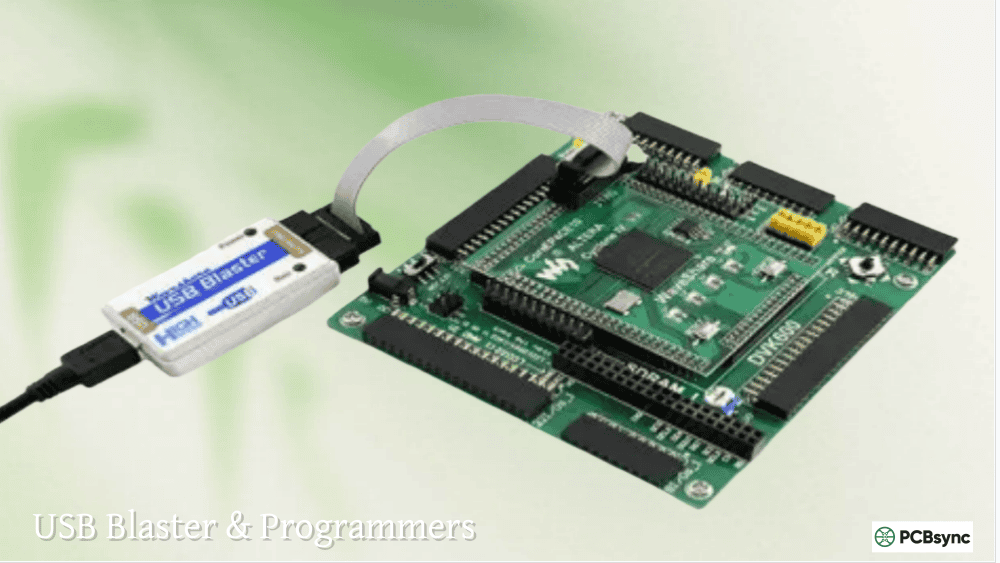
Connect USB cable from PC to the USB-Blaster port on the board
Connect 12V power adapter
Turn on the board using the red power switch
Installing USB-Blaster Drivers
The USB-Blaster driver installation process varies by operating system:
Windows 10/11:
Connect the board via USB
Open Device Manager
Locate “Unknown Device” or “USB-Blaster”
Right-click → Update Driver
Browse to: <Quartus Install Path>\drivers\usb-blaster
Complete the wizard
Linux: Create a udev rule file /etc/udev/rules.d/51-altera-usb-blaster.rules:
The DE2-115 ships with a preloaded demonstration bitstream. To verify board functionality:
Connect VGA monitor to the VGA port
Connect headphones to the line-out jack
Ensure SW19 (RUN/PROG) is in the RUN position
Power cycle the board
You should see a test pattern on the VGA display and hear audio tones when manipulating the switches. This confirms the major subsystems are operational.
Your First Custom Design
Here’s a simple Verilog design to verify your toolchain works correctly:
// Button to green LED mapping (active low inverted)
assign LEDG[3:0] = ~KEY;
assign LEDG[8:4] = 5’b0;
endmodule
To implement this design:
Create a new Quartus project targeting EP4CE115F29C7
Add the Verilog file to your project
Import pin assignments from the DE2-115.qsf file (available from Terasic)
Compile the design
Program via the Programmer tool
Working with the DE2-115 LCD Display
The onboard DE2-115 LCD is a 16×2 character display based on the HD44780 controller. It’s connected directly to FPGA pins, requiring you to implement the LCD controller logic in your design.
LCD Pin Connections
Signal
FPGA Pin
Function
LCD_DATA[7:0]
Various
Bidirectional data bus
LCD_EN
PIN_L4
Enable strobe
LCD_RS
PIN_L3
Register select (0=command, 1=data)
LCD_RW
PIN_L5
Read/Write select
LCD_ON
PIN_L6
Backlight control
LCD_BLON
—
Not used on DE2-115
LCD Initialization Sequence
The HD44780 requires a specific initialization sequence:
Wait 15ms after power-on
Send Function Set command (0x38 for 8-bit, 2-line)
Wait 4.1ms
Repeat Function Set
Wait 100μs
Send Function Set again
Configure display: Display ON, Cursor settings
Clear display
Set entry mode
Timing is critical—the LCD requires minimum pulse widths and setup/hold times that must be respected in your HDL implementation.
Example LCD Controller
Several open-source LCD controllers for the DE2-115 are available on GitHub:
amanmibra/lcd-de2-115 – Basic LCD driver in Verilog
SayidHosseini/DE2-115_VHDL_PS2-CLCD – PS/2 keyboard to LCD interface
For Nios II-based designs, the Intel FPGA University Program provides a complete LCD peripheral core with software drivers.
The versatility of the FPGA Altera DE2-115 makes it suitable for projects ranging from introductory digital logic to advanced system-on-chip designs.
Beginner Projects
LED Pattern Generator Create various LED animations using the 18 red and 9 green LEDs. Implement counters, shift registers, and state machines to produce different patterns.
7-Segment Display Counter Build a multi-digit counter displayed on the eight 7-segment displays. Add features like count direction control via switches and reset via buttons.
Simple Calculator Use switches for numeric input, buttons for operations, and 7-segment displays for results. A good introduction to arithmetic circuits.
Intermediate Projects
VGA Graphics Controller Implement a VGA controller supporting 640×480 resolution. The DE2-115 includes 8-bit DACs for RGB output, enabling 256-color displays.
Audio Synthesizer The onboard Wolfson WM8731 codec supports 24-bit audio at up to 96kHz. Build a simple tone generator or waveform synthesizer.
UART Communication Use the RS-232 port to communicate with a PC. Implement a simple command processor that responds to serial commands.
SD Card Interface Read and write files to SD cards. Start with SPI mode for simplicity, then advance to 4-bit SD mode for higher throughput.
Advanced Projects
Nios II Soft Processor System Implement Intel’s Nios II processor with peripherals including:
SDRAM controller (128MB)
JTAG UART for debugging
Timer and interrupt controller
GPIO for switches and LEDs
LCD controller
The Intel FPGA University Program provides complete reference designs for the DE2-115 that implement a full computer system.
Digital Camera System Connect the TRDB-D5M camera daughter card and implement:
Image capture and buffering
Real-time video display on VGA
Image processing filters (edge detection, color conversion)
Frame buffer in SDRAM
Network Applications Utilize the dual Gigabit Ethernet ports for:
For the best experience with the DE2-115, I recommend Quartus Prime Lite 18.1. It provides modern features while maintaining excellent compatibility with existing example designs.
Frequently Asked Questions (FAQs)
What Quartus version should I use with the DE2-115?
For the Altera DE2-115, Quartus Prime Lite Edition version 18.1 offers the best balance of features and stability. It’s free, supports all Cyclone IV devices, and includes ModelSim for simulation. Newer versions (20.1+) also work but may have compatibility issues with older example projects. Avoid versions newer than 20.1 if you need ModelSim, as Intel transitioned to Questa which requires a free license.
Can I use the DE2-115 for commercial product development?
Yes, the Terasic DE2-115 can be used for prototyping commercial products. However, for production, you’ll typically design a custom PCB with only the components your application requires. The DE2-115’s strength is in development and education—it provides all the interfaces you might need during the design phase, but its size and cost make it impractical for embedding in final products.
How do I get academic pricing for the DE2-115?
To obtain the DE2-115 price at academic rates ($423 vs $779), you must verify your educational affiliation through Terasic’s website. Students need to provide a valid .edu email address or documentation proving enrollment. Educators and institutions can establish accounts for bulk purchases. The verification process typically takes 1-2 business days.
Is the DE2-115 suitable for learning FPGA development?
Absolutely. The DE2-115 FPGA board is specifically designed for education and remains one of the most popular choices for university digital logic and computer architecture courses. The extensive documentation, example designs from Intel’s University Program, and decade-long community support make it an excellent learning platform. The variety of onboard peripherals lets students progress from simple LED exercises to complex system-on-chip designs without purchasing additional hardware.
What’s the difference between the DE2-115 and DE2-70?
Both boards use Cyclone-series FPGAs, but the DE2-115 offers significant upgrades: a larger FPGA (114,480 vs 68,416 LEs), more SDRAM (128MB vs 64MB), dual Gigabit Ethernet (vs single 100Mbps), and an HSMC expansion connector. The DE2-70 used Cyclone II, while the DE2-115 uses the more power-efficient Cyclone IV. For new purchases, the DE2-115 is the clear choice, though the DE2-70 remains capable for many projects.
Troubleshooting Common DE2-115 Issues
Working with the DE2-115 over the years, I’ve encountered several common issues that trip up new users. Here’s how to resolve them.
Board Not Detected by Quartus Programmer
Symptoms: The Programmer shows “No Hardware” or cannot find USB-Blaster.
Solutions:
Verify USB-Blaster drivers are correctly installed
Check that SW19 is in the correct position (RUN for JTAG programming)
Try a different USB port—some USB 3.0 ports have compatibility issues
On Linux, ensure udev rules are properly configured
Power cycle the board after connecting USB
Compilation Succeeds but Design Doesn’t Work
Common causes:
Incorrect pin assignments—always import the official DE2-115.qsf file
Clock constraints missing—add SDC constraints for timing closure
Active-low signals not inverted—KEY buttons are active-low on this board
Unused pins floating—configure unused pins in Device Settings
LCD Display Shows Garbage or Nothing
The DE2-115 LCD requires proper initialization timing:
Ensure sufficient delay after power-on (minimum 15ms)
Verify LCD_ON signal is driven high for backlight
Check that enable pulse widths meet HD44780 specifications
Confirm data setup and hold times are respected
SDRAM Access Failures
SDRAM issues often stem from:
Incorrect refresh timing
Clock/data phase alignment problems
Missing initialization sequence
Improper burst length configuration
Use Terasic’s verified SDRAM controller IP as a starting point rather than writing your own from scratch.
Power Consumption and Thermal Considerations
Understanding power characteristics helps when designing complex systems on the FPGA Altera DE2-115.
Typical Power Consumption
Design Complexity
Approximate Current (12V)
Minimal (LEDs only)
200-300 mA
Moderate (VGA + Audio)
400-500 mA
Full System (Nios II + SDRAM)
600-800 mA
Maximum Load
~1.2 A
The included 12V/2A power adapter provides adequate headroom for even complex designs. However, if you’re using HSMC daughter cards, verify that combined power requirements remain within limits.
Thermal Management
The Cyclone IV EP4CE115 can generate significant heat under heavy utilization:
Normal operation: FPGA surface temperature 40-50°C
High utilization: Up to 70°C without additional cooling
The board has no heatsink—rely on ambient convection
For sustained high-utilization applications, consider adding a small heatsink to the FPGA package or improving airflow around the board.
Conclusion
The Altera DE2-115 has earned its reputation as a premier educational FPGA platform through years of proven use in universities worldwide. Despite being based on the Cyclone IV architecture—not Intel’s latest—the board’s comprehensive peripheral complement and extensive software support make it remain relevant for learning and prototyping.
For students and educators evaluating FPGA development boards, the Terasic DE2-115 offers unmatched value at academic pricing. The 114,480 logic elements accommodate substantial designs, the 128MB SDRAM supports complex Nios II applications, and the dual Gigabit Ethernet enables networking projects that smaller boards cannot handle.
Whether you’re implementing your first LED blinker or building a complete soft-processor system with camera input and VGA output, the DE2-115 FPGA provides the resources you need. The investment in learning this platform translates directly to skills applicable across all Intel FPGA families—the fundamental concepts of digital design, HDL coding, and timing closure remain constant regardless of the specific device.
If you’re ready to begin your FPGA journey, download Quartus Prime Lite, obtain a DE2-115 board, and start with the simple examples provided in Intel’s University Program materials. Within a few weeks, you’ll progress from basic combinational logic to sequential designs, and eventually to complete embedded systems that showcase what programmable logic can accomplish.
Suggested Meta Descriptions:
Option 1 (155 characters): “Complete guide to the Altera DE2-115 FPGA board: specifications, academic vs commercial pricing, LCD display usage, Nios II projects, and getting started tutorials.”
Option 2 (150 characters): “Terasic DE2-115 FPGA development board guide covering Cyclone IV specs, DE2-115 price comparison, project ideas, LCD interfacing, and setup instructions.”
Option 3 (158 characters): “Learn everything about the DE2-115 FPGA board: detailed features, where to buy at academic pricing, VGA/LCD projects, Quartus setup, and Nios II development tips.”
Inquire: Call 0086-755-23203480, or reach out via the form below/your sales contact to discuss our design, manufacturing, and assembly capabilities.
Quote: Email your PCB files to Sales@pcbsync.com (Preferred for large files) or submit online. We will contact you promptly. Please ensure your email is correct.
Notes: For PCB fabrication, we require PCB design file in Gerber RS-274X format (most preferred), *.PCB/DDB (Protel, inform your program version) format or *.BRD (Eagle) format. For PCB assembly, we require PCB design file in above mentioned format, drilling file and BOM. Click to download BOM template To avoid file missing, please include all files into one folder and compress it into .zip or .rar format.


