Inquire: Call 0086-755-23203480, or reach out via the form below/your sales contact to discuss our design, manufacturing, and assembly capabilities.
Quote: Email your PCB files to Sales@pcbsync.com (Preferred for large files) or submit online. We will contact you promptly. Please ensure your email is correct.
Notes: For PCB fabrication, we require PCB design file in Gerber RS-274X format (most preferred), *.PCB/DDB (Protel, inform your program version) format or *.BRD (Eagle) format. For PCB assembly, we require PCB design file in above mentioned format, drilling file and BOM. Click to download BOM template To avoid file missing, please include all files into one folder and compress it into .zip or .rar format.
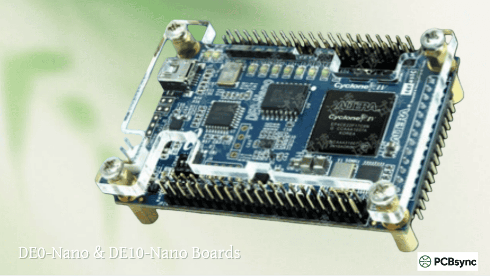
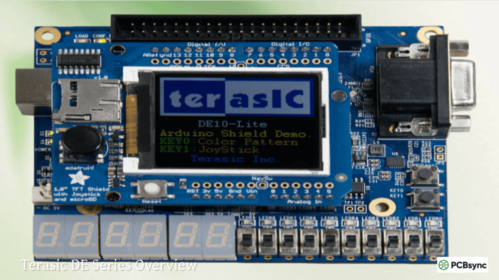
DE0-Nano vs DE10-Nano: Complete Guide to Terasic Nano FPGA Boards
If you’ve been researching Intel/Altera FPGA development boards, you’ve probably come across two boards that share similar names but serve very different purposes: the DE0-Nano and the DE10-Nano. As someone who has designed dozens of FPGA-based systems over the past decade, I’ve worked extensively with both of these Terasic boards and understand the confusion that their naming creates for engineers and hobbyists alike. This comprehensive guide will help you understand exactly what each board offers and which one is right for your specific project needs.
The Altera DE0-Nano and Altera DE10-Nano represent two different generations and philosophies of FPGA development. The DE0-Nano FPGA board is a compact, lightweight platform built around the Cyclone IV FPGA, designed primarily for portable projects and educational use. The Altera DE10-Nano, on the other hand, is a more powerful System-on-Chip (SoC) platform featuring a Cyclone V FPGA with integrated dual-core ARM Cortex-A9 processor, making it suitable for complex embedded applications and the wildly popular MiSTer FPGA retro gaming project.
Understanding the differences between these DE Terasic boards is essential before making a purchase decision. Whether you’re a student learning digital design fundamentals, a hobbyist building robotics projects, or a professional engineer prototyping industrial IoT systems, choosing the right Altera Nano board will significantly impact your development experience and project outcomes.
The DE0-Nano Terasic board was introduced in 2011 as part of Altera’s University Program, designed specifically to provide an affordable, compact FPGA development platform for educational institutions and portable design projects. Measuring just 49mm by 75.2mm and weighing approximately 40 grams, the DE0 Nano is one of the smallest full-featured FPGA development boards available on the market, making it exceptionally well-suited for robotics applications and embedded designs where size and weight are critical constraints.
DE0-Nano Technical Specifications and Features
At the heart of the DE0 FPGA board sits an Altera Cyclone IV EP4CE22F17C6N FPGA, featuring 22,320 logic elements (LEs), 594 Kbits of embedded memory, 66 embedded multipliers, and 4 PLLs. While these specifications might seem modest compared to newer FPGA families, they’re more than sufficient for learning digital design, implementing soft processors like Nios II, and building real-world control systems. The Cyclone IV family remains popular in 2024 because of its excellent power efficiency, mature toolchain support, and proven reliability across countless production deployments.
Key features of the DE0-Nano Terasic board include:
32MB SDRAM (16Mx16 bits) for data storage and frame buffering applications
2KB I2C EEPROM for non-volatile configuration storage
16MB EPCS16 serial configuration device for FPGA programming
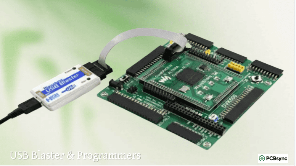
Built-in USB Blaster for JTAG programming (no external programmer required)
8-channel 12-bit ADC (NS ADC128S022) for analog sensor interfacing
3-axis accelerometer (ADXL345) with 13-bit resolution
Two 40-pin GPIO expansion headers (active driving range: 3.3V TTL)
8 user LEDs, 2 push-buttons, and 4 DIP switches
Multiple power options: USB Mini-AB, 2-pin external header, or DC 5V pins
Ideal Use Cases for the Altera DE0-Nano
The DE0 Altera board excels in scenarios where portability, low power consumption, and cost-effectiveness are priorities. University professors love it for teaching digital logic design because students can take it home and experiment without worrying about expensive equipment. The built-in accelerometer and ADC make it perfect for sensor fusion projects, robotics control systems, and IoT prototypes. I’ve personally used the DE0-Nano FPGA in several quadcopter flight controller projects where the lightweight form factor was essential for maintaining flight characteristics.
The two 40-pin GPIO headers provide access to 72 I/O pins, which is sufficient for interfacing with motors, servos, displays, and various sensors. Terasic offers numerous daughter cards that plug directly into these headers, including motor control boards, camera interfaces, and wireless communication modules. This expandability makes the DE0 Terasic platform versatile enough for projects ranging from simple LED blinkers to complex real-time control systems.
What is the Altera DE10-Nano Development Board?
The Altera DE10-Nano represents a significant evolution in Terasic’s development board lineup, combining the flexibility of FPGA programmable logic with the processing power of a hard ARM processor in a single System-on-Chip (SoC) package. Released as part of Intel’s push into the SoC FPGA market, the Altera Terasic DE10-Nano has become the foundation for one of the most exciting developments in retro gaming: the MiSTer FPGA project, which uses the board to accurately recreate vintage computer and gaming hardware through hardware emulation.
DE10-Nano Technical Specifications and Architecture
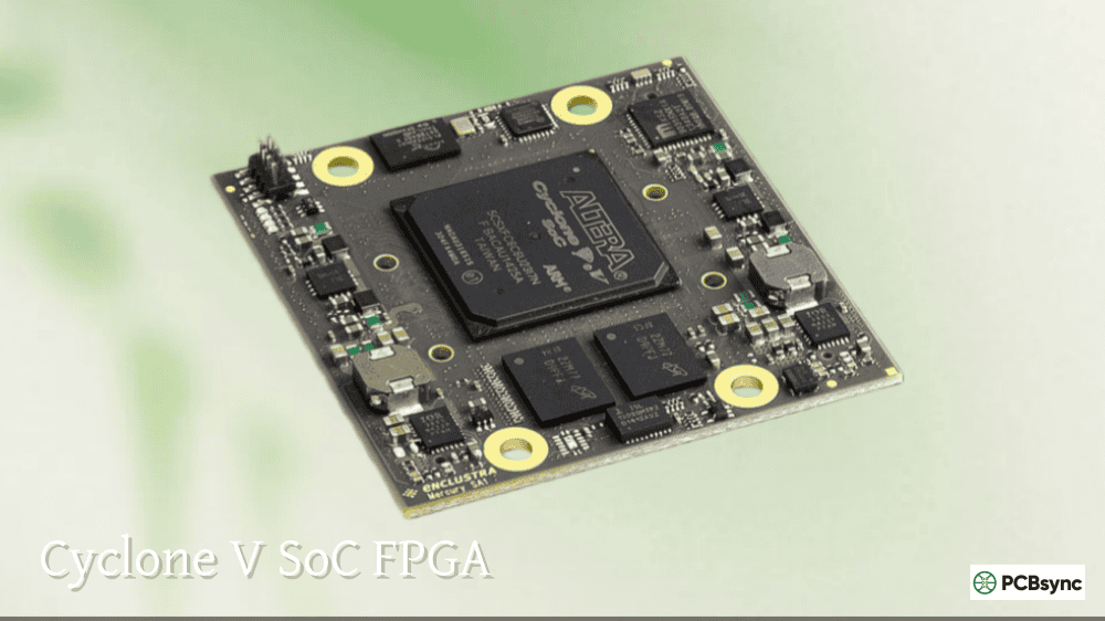
The DE10-Nano features an Intel (formerly Altera) Cyclone V SE 5CSEBA6U23I7 SoC FPGA, which integrates both FPGA fabric and a Hard Processor System (HPS) on a single die. This architectural approach allows developers to implement time-critical logic in the FPGA while running complex software stacks (including full Linux distributions) on the ARM cores. The tight integration between the HPS and FPGA fabric through high-bandwidth interconnects enables unprecedented flexibility in system design.
The FPGA fabric specifications include:
110,000 programmable logic elements (approximately 5x more than DE0-Nano)
5,570 Kbits of embedded memory (roughly 9x more than DE0-Nano)
112 variable-precision DSP blocks optimized for signal processing
6 fractional PLLs for flexible clock generation
The Hard Processor System (HPS) features:
Dual-core ARM Cortex-A9 MPCore processor running at 800MHz
1GB DDR3 SDRAM with 32-bit data bus (HPS exclusive)
Gigabit Ethernet PHY with RJ45 connector for network connectivity
USB OTG port (Micro-AB connector) for peripherals
Micro SD card socket for Linux boot and storage
UART-to-USB bridge for serial console access
Full HD HDMI transmitter (directly accessible from FPGA fabric)
DE10-Nano Expansion and Connectivity Options
One of the standout features of the Altera DE10 Nano is its Arduino-compatible expansion header, which allows direct connection to hundreds of existing Arduino shields and accessories. This dramatically lowers the barrier to entry for makers who are already familiar with the Arduino ecosystem but want to explore the power of FPGA-accelerated computing. Additionally, the board includes two 40-pin GPIO headers similar to the DE0-Nano, providing ample I/O for custom expansion designs.
The LTC 2×7 expansion header on the DE10-Nano deserves special mention, as it provides a direct connection to Linear Technology’s DC934A daughter card for high-resolution analog-to-digital and digital-to-analog conversion. This makes the board particularly attractive for precision measurement, audio processing, and software-defined radio applications where analog signal quality is paramount.
DE0-Nano vs DE10-Nano: Detailed Specifications Comparison
Understanding the technical differences between these two Terasic Nano FPGA boards is crucial for making an informed purchase decision. The following comparison table highlights the key specifications that matter most for typical development scenarios.
Specification
DE0-Nano (Cyclone IV)
DE10-Nano (Cyclone V SoC)
FPGA Device
EP4CE22F17C6N
5CSEBA6U23I7
Logic Elements
22,320 LEs
110,000 LEs
Embedded Memory
594 Kbits
5,570 Kbits
DSP Blocks
66 multipliers
112 DSP blocks
ARM Processor
None
Dual-core Cortex-A9 @ 800MHz
External RAM
32MB SDRAM
1GB DDR3 (HPS)
Video Output
None (via GPIO)
HDMI (Full HD 1080p)
Ethernet
None
Gigabit Ethernet
USB
Mini-AB (programming only)
USB OTG + USB-UART
SD Card
None
Micro SD slot
Arduino Header
No
Yes (Uno R3 compatible)
ADC
8-ch 12-bit
LTC expansion header
Accelerometer
ADXL345 (3-axis)
ADXL345 (3-axis)
Board Size
49mm x 75mm
70mm x 110mm
Weight
~40 grams
~100 grams
Price (2024)
~$108 USD
~$225 USD
The DE10-Nano and MiSTer FPGA: A Revolutionary Retro Gaming Platform
One of the most compelling reasons people seek out the Altera DE10-Nano today has nothing to do with traditional FPGA development—it’s the MiSTer project. MiSTer is an open-source hardware recreation platform that uses the DE10-Nano’s Cyclone V SoC to accurately emulate vintage computers, game consoles, and arcade systems through actual hardware simulation rather than software emulation. This distinction is crucial: while software emulators approximate how original hardware behaves, FPGA-based systems like MiSTer physically reconfigure their logic gates to match the original silicon, resulting in cycle-accurate behavior with minimal latency.
Why the DE10-Nano Became the MiSTer Standard
The DE10-Nano Quartus development environment and the board’s specific hardware configuration made it an ideal platform for the MiSTer project. The 110,000 logic elements are sufficient to recreate complex systems like the Neo Geo, Sega Genesis, Super Nintendo, and even early 32-bit systems. The 1GB DDR3 RAM provides ample storage for game ROMs and system data, while the HDMI output enables direct connection to modern displays with upscaling up to 1080p.
The MiSTer ecosystem has grown substantially around the DE10-Nano, with numerous add-on boards available to extend functionality. The SDRAM expansion module (32MB or 128MB) is essential for running certain cores that require lower-latency memory access than the DDR3 can provide. The I/O board adds VGA output for connecting to CRT monitors, 3.5mm audio jacks, and additional expansion options. A USB hub board provides multiple USB ports for controllers and keyboards, transforming the DE10-Nano into a complete retro gaming system.
MiSTer Supported Systems on DE10-Nano
The MiSTer project supports an impressive range of classic gaming and computing platforms through dedicated “cores” (FPGA configurations). Currently supported systems include the Nintendo Entertainment System, Super Nintendo, Sega Genesis/Mega Drive, Sega Master System, TurboGrafx-16, Neo Geo (AES and MVS), Game Boy, Game Boy Advance, Atari 2600, Commodore 64, Amiga, Atari ST, and dozens of arcade boards. Development is ongoing for even more complex systems, with PlayStation 1 and Nintendo 64 cores under active development by the community.
Setting Up DE0-Nano and DE10-Nano with Quartus Prime Software
Both the DE0-Nano and DE10-Nano are programmed using Intel’s Quartus Prime development software, though the setup procedures differ slightly due to the additional SoC components on the DE10. Understanding the complete setup process is essential for getting productive quickly with either board.
Installing Quartus Prime for DE0-Nano Development
Download Quartus Prime Lite Edition from Intel’s FPGA Software Download Center (free, no license required)
Select the Cyclone IV device family support during installation
Install the USB Blaster driver from the Quartus installation directory when prompted
Connect the DE0-Nano via USB Mini-AB cable to power and establish programming connection
Create a new project targeting device EP4CE22F17C6 (the DE0-Nano’s FPGA)
Import pin assignment files from Terasic’s DE0-Nano resource page to match board layout
DE10-Nano Quartus and SoC EDS Setup
The DE10-Nano Quartus setup is more involved due to the SoC architecture. In addition to Quartus Prime (with Cyclone V device support), you’ll also need Intel’s SoC Embedded Development Suite (SoC EDS) if you plan to develop software for the ARM cores. The SoC EDS includes the ARM Development Studio (DS-5), compiler toolchains, and utilities for creating preloader and U-Boot bootloader images.
Download and install Quartus Prime Lite Edition with Cyclone V device support
Download and install Intel SoC FPGA Embedded Development Suite (EDS)
Install USB Blaster II driver (different from DE0-Nano’s USB Blaster)
Connect DE10-Nano via USB cable to J13 connector for JTAG programming
Download reference designs from Terasic or Intel GitHub repositories
Important Note: When creating projects for the DE10-Nano, always select device 5CSEBA6U23I7 and NOT 5CSEBA6U23I7DK. The DK variant causes issues with preloader generation and can result in boards that fail to boot properly. This is a common mistake that wastes hours of debugging time.
DE0-Nano vs DE10-Nano: Which Terasic Board Should You Choose?
Choosing between the DE0-Nano and DE10-Nano ultimately depends on your specific project requirements, budget, and learning objectives. Both boards are excellent platforms with active community support and extensive documentation, but they serve distinctly different use cases.
Choose the DE0-Nano FPGA Board If You Need:
A compact, lightweight board for portable or embedded applications
An affordable entry point to learn FPGA development fundamentals
Built-in analog-to-digital conversion for sensor interfacing projects
A board for robotics applications where size and weight matter
Simple FPGA-only designs without processor complexity
University coursework or personal educational projects
Choose the Altera DE10-Nano If You Need:
Substantially more logic capacity for complex designs (5x more LEs)
Integrated ARM processor for running Linux or real-time operating systems
HDMI video output for display-based applications
Network connectivity via built-in Gigabit Ethernet
A platform for the MiSTer FPGA retro gaming project
Arduino shield compatibility for rapid prototyping
Industrial IoT development with heterogeneous computing capabilities
Project Ideas for DE0-Nano and DE10-Nano FPGA Boards
Both the DE0-Nano and DE10-Nano provide excellent platforms for a wide range of projects spanning from educational exercises to professional prototypes. The project possibilities are virtually unlimited, constrained only by the available logic resources and peripherals. Here’s a comprehensive collection of project ideas organized by complexity and board suitability to help inspire your next FPGA development adventure.
DE0-Nano Beginner and Intermediate Projects
Digital Logic Learning: LED chaser patterns, 7-segment display drivers, combinational logic circuits, state machines, and counters
Nios II Soft Processor: Implement Intel’s soft CPU core for embedded programming experience with C/C++ applications
Motor Control Systems: PWM generation for servo motors, DC motor speed control with H-bridge interfacing, and stepper motor drivers
Sensor Fusion Projects: Combine accelerometer data with external sensors using the ADC for tilt measurement, motion detection, and orientation tracking
VGA Display Driver: Generate VGA signals using GPIO pins for graphics output, retro game development, and oscilloscope displays
UART and SPI Communication: Implement serial protocols for computer communication, sensor interfacing, and data logging applications
Quadcopter Flight Controller: Use the compact form factor and built-in accelerometer to create custom drone stabilization systems
DE10-Nano Advanced Projects
MiSTer FPGA Retro Gaming: Build a complete retro gaming system with hardware-accurate emulation of classic consoles and arcade machines
Embedded Linux Development: Run full Debian/Ubuntu distributions on the ARM cores while accelerating tasks in the FPGA fabric
Hardware Acceleration: Offload compute-intensive tasks from ARM to FPGA fabric for image processing, encryption, and mathematical operations
Software Defined Radio: Implement radio protocols with DSP processing in FPGA for amateur radio, FM receivers, and spectrum analyzers
Real-time Image Processing: Video processing pipelines with HDMI output for edge detection, color correction, and object tracking
Neural Network Inference: Accelerate machine learning models using FPGA logic for real-time AI applications
Network Protocol Implementation: Leverage Gigabit Ethernet for custom protocol development, packet inspection, and network appliance prototyping
Troubleshooting Common DE0-Nano and DE10-Nano Issues
Even experienced FPGA developers encounter setup and configuration issues when working with development boards. Here are solutions to the most common problems I’ve encountered over years of working with Terasic’s Nano series boards, along with tips that will save you hours of debugging frustration.
USB Blaster Not Detected in Quartus Programmer
This is the most common issue for both boards. First, verify the board is powered (LEDs should be visible). On Windows, check Device Manager for an unrecognized USB device and manually install the driver from your Quartus installation directory (typically quartus/drivers/usb-blaster). On Linux, create udev rules to allow non-root access to the USB Blaster device. If using the DE10-Nano, ensure you’re using the correct USB port (J13) for programming, not the USB OTG port. Sometimes simply power cycling the board and restarting Quartus resolves detection issues.
DE10-Nano Fails to Boot Linux from SD Card
The most common cause is incorrect MSEL DIP switch settings. For Linux boot from SD card, set the MSEL switches (SW10) according to the user manual configuration for your specific boot mode. Verify the SD card image was written correctly using a tool like Balena Etcher rather than simple file copy. Check the serial console output via the UART-to-USB connection for boot messages and error codes. If the SD card was working previously, try reformatting and re-imaging it, as SD cards can develop bad sectors over time.
FPGA Configuration Fails with ‘JTAG Chain Broken’ Error
This error typically indicates a communication problem between the USB Blaster and the FPGA. Verify the board power supply is stable and within specification (5V for both boards). Check that no other software is accessing the JTAG interface. On the DE10-Nano, remember that both the FPGA and HPS appear in the JTAG chain – ensure you’re targeting the correct device. Try reducing the TCK clock frequency in Quartus Programmer settings if you’re using long cables or experiencing noise issues. Sometimes switching to a different USB port (preferably USB 2.0 rather than USB 3.0) resolves compatibility issues.
Essential Resources and Downloads for Terasic FPGA Boards
MiSTer Addons Shop: https://misteraddons.com/ (pre-assembled boards and accessories)
Where to Buy DE0-Nano and DE10-Nano
Terasic Direct: Best prices, academic discounts available for students/educators
DigiKey: Fast shipping, good stock availability in North America
Mouser Electronics: Global shipping, competitive pricing
Element14/Farnell: Good availability in Europe and Asia-Pacific regions
Frequently Asked Questions About Terasic Nano FPGA Boards
Can I use the DE0-Nano for the MiSTer project instead of the DE10-Nano?
No, the DE0-Nano cannot run MiSTer. The MiSTer project requires the specific Cyclone V SoC FPGA with its integrated ARM processor, 1GB DDR3 memory, and HDMI output that only the DE10-Nano provides. The DE0-Nano’s Cyclone IV FPGA has insufficient logic elements (22K vs 110K), lacks the ARM processor needed to run the Linux-based MiSTer framework, and has no HDMI output. There is no alternative board currently supported by the MiSTer project other than the DE10-Nano (though a community project called MiSTer Pi recently emerged as a lower-cost alternative using the same Cyclone V FPGA).
Is the DE0-Nano still worth buying in 2024 or should I get the DE10-Nano instead?
The DE0-Nano remains an excellent choice for specific use cases despite being based on older technology. If you’re learning FPGA fundamentals, building robotics projects, or need a compact embedded platform, the DE0-Nano’s lower price (~$108 vs ~$225), smaller size, built-in ADC, and simpler toolchain make it the better choice. The DE10-Nano’s complexity can actually slow down beginners who need to learn FPGA basics before tackling SoC development. However, if you need more logic capacity, want networking capabilities, or plan to run Linux on your FPGA board, the DE10-Nano is the clear winner.
What version of Quartus Prime should I use with these boards?
Both boards work with Quartus Prime Lite Edition, which is free and doesn’t require a license. For the DE0-Nano (Cyclone IV), almost any recent Quartus version from 13.0 through the latest release will work well. For the DE10-Nano (Cyclone V SoC), Quartus Prime 18.1 or later is recommended, with versions 20.1 and 21.1 being particularly stable. Some users report issues with the very latest Quartus releases when working with older reference designs, so check compatibility with your specific project requirements. The MiSTer project typically recommends specific Quartus versions in their documentation.
Do I need to buy a separate USB Blaster programmer for these boards?
No, both the DE0-Nano and DE10-Nano include built-in programming hardware. The DE0-Nano has an integrated USB Blaster circuit that handles JTAG programming through its USB Mini-AB connector. The DE10-Nano includes a USB Blaster II circuit (accessible through the J13 connector) that supports both FPGA and HPS JTAG chains. You only need to install the appropriate driver from your Quartus installation, connect the USB cable, and you’re ready to program. Separate USB Blaster cables are only needed if you want to program multiple boards simultaneously or need the longer cable reach that standalone programmers provide.
Can I run Linux on the DE0-Nano?
Not directly. The DE0-Nano doesn’t have a hard ARM processor like the DE10-Nano, so it cannot run Linux in the traditional sense. However, you can implement a soft processor core like Nios II in the FPGA fabric and run uClinux (a microcontroller-optimized Linux variant) on it, though this is significantly slower than the DE10-Nano’s 800MHz ARM cores and provides limited functionality. For serious Linux development on FPGA, the DE10-Nano or similar SoC boards like the DE0-Nano-SoC (a different board with Cyclone V SoC) are much better choices.
Conclusion: Making Your Terasic Nano FPGA Board Decision
The DE0-Nano and DE10-Nano represent two excellent options in Terasic’s extensive FPGA development board portfolio, each serving distinct market segments and use cases. The DE0-Nano FPGA board continues to excel as an affordable, compact platform for education, robotics, and portable applications where its small form factor and built-in sensors provide unique advantages. Meanwhile, the Altera DE10-Nano has established itself as the definitive platform for complex SoC development and the thriving MiSTer FPGA retro gaming community.
For beginners just starting their FPGA journey, I typically recommend starting with the DE0-Nano due to its lower complexity and cost, then graduating to the DE10-Nano once you’ve mastered the fundamentals and want to explore SoC development or join the MiSTer community. For experienced engineers or those with specific requirements for ARM processing, networking, or HDMI output, the DE10-Nano delivers exceptional value given its sophisticated feature set and the incredible ecosystem that has grown around it.
Whichever board you choose, you’ll be joining a vibrant community of FPGA enthusiasts, educators, and professional engineers who continue to push the boundaries of what’s possible with programmable logic. Both the DE0 Terasic and DE10 Terasic platforms benefit from years of refinement, extensive documentation, and the backing of Intel’s comprehensive Quartus Prime toolchain. Your choice between these Altera Nano boards will serve you well for years of productive development and learning.
Inquire: Call 0086-755-23203480, or reach out via the form below/your sales contact to discuss our design, manufacturing, and assembly capabilities.
Quote: Email your PCB files to Sales@pcbsync.com (Preferred for large files) or submit online. We will contact you promptly. Please ensure your email is correct.
Notes: For PCB fabrication, we require PCB design file in Gerber RS-274X format (most preferred), *.PCB/DDB (Protel, inform your program version) format or *.BRD (Eagle) format. For PCB assembly, we require PCB design file in above mentioned format, drilling file and BOM. Click to download BOM template To avoid file missing, please include all files into one folder and compress it into .zip or .rar format.


